KR20200059570A - 정전 척, 및 그를 포함하는 플라즈마 처리 장치 - Google Patents
정전 척, 및 그를 포함하는 플라즈마 처리 장치 Download PDFInfo
- Publication number
- KR20200059570A KR20200059570A KR1020180144455A KR20180144455A KR20200059570A KR 20200059570 A KR20200059570 A KR 20200059570A KR 1020180144455 A KR1020180144455 A KR 1020180144455A KR 20180144455 A KR20180144455 A KR 20180144455A KR 20200059570 A KR20200059570 A KR 20200059570A
- Authority
- KR
- South Korea
- Prior art keywords
- plate
- electrostatic chuck
- disposed
- ring
- inner plate
- Prior art date
- Legal status (The legal status is an assumption and is not a legal conclusion. Google has not performed a legal analysis and makes no representation as to the accuracy of the status listed.)
- Granted
Links
Images



Classifications
-
- H—ELECTRICITY
- H01—ELECTRIC ELEMENTS
- H01J—ELECTRIC DISCHARGE TUBES OR DISCHARGE LAMPS
- H01J37/00—Discharge tubes with provision for introducing objects or material to be exposed to the discharge, e.g. for the purpose of examination or processing thereof
- H01J37/32—Gas-filled discharge tubes
- H01J37/32431—Constructional details of the reactor
- H01J37/32532—Electrodes
-
- H—ELECTRICITY
- H10—SEMICONDUCTOR DEVICES; ELECTRIC SOLID-STATE DEVICES NOT OTHERWISE PROVIDED FOR
- H10P—GENERIC PROCESSES OR APPARATUS FOR THE MANUFACTURE OR TREATMENT OF DEVICES COVERED BY CLASS H10
- H10P72/00—Handling or holding of wafers, substrates or devices during manufacture or treatment thereof
- H10P72/70—Handling or holding of wafers, substrates or devices during manufacture or treatment thereof for supporting or gripping
- H10P72/72—Handling or holding of wafers, substrates or devices during manufacture or treatment thereof for supporting or gripping using electrostatic chucks
- H10P72/722—Details of electrostatic chucks
-
- H01L21/6833—
-
- H—ELECTRICITY
- H01—ELECTRIC ELEMENTS
- H01J—ELECTRIC DISCHARGE TUBES OR DISCHARGE LAMPS
- H01J37/00—Discharge tubes with provision for introducing objects or material to be exposed to the discharge, e.g. for the purpose of examination or processing thereof
- H01J37/32—Gas-filled discharge tubes
- H01J37/32431—Constructional details of the reactor
- H01J37/32715—Workpiece holder
-
- H01L21/6835—
-
- H01L21/68721—
-
- H—ELECTRICITY
- H05—ELECTRIC TECHNIQUES NOT OTHERWISE PROVIDED FOR
- H05H—PLASMA TECHNIQUE; PRODUCTION OF ACCELERATED ELECTRICALLY-CHARGED PARTICLES OR OF NEUTRONS; PRODUCTION OR ACCELERATION OF NEUTRAL MOLECULAR OR ATOMIC BEAMS
- H05H1/00—Generating plasma; Handling plasma
- H05H1/24—Generating plasma
- H05H1/46—Generating plasma using applied electromagnetic fields, e.g. high frequency or microwave energy
-
- H—ELECTRICITY
- H10—SEMICONDUCTOR DEVICES; ELECTRIC SOLID-STATE DEVICES NOT OTHERWISE PROVIDED FOR
- H10P—GENERIC PROCESSES OR APPARATUS FOR THE MANUFACTURE OR TREATMENT OF DEVICES COVERED BY CLASS H10
- H10P50/00—Etching of wafers, substrates or parts of devices
- H10P50/20—Dry etching; Plasma etching; Reactive-ion etching
- H10P50/24—Dry etching; Plasma etching; Reactive-ion etching of semiconductor materials
- H10P50/242—Dry etching; Plasma etching; Reactive-ion etching of semiconductor materials of Group IV materials
-
- H—ELECTRICITY
- H10—SEMICONDUCTOR DEVICES; ELECTRIC SOLID-STATE DEVICES NOT OTHERWISE PROVIDED FOR
- H10P—GENERIC PROCESSES OR APPARATUS FOR THE MANUFACTURE OR TREATMENT OF DEVICES COVERED BY CLASS H10
- H10P72/00—Handling or holding of wafers, substrates or devices during manufacture or treatment thereof
- H10P72/70—Handling or holding of wafers, substrates or devices during manufacture or treatment thereof for supporting or gripping
- H10P72/74—Handling or holding of wafers, substrates or devices during manufacture or treatment thereof for supporting or gripping using temporarily an auxiliary support
-
- H—ELECTRICITY
- H10—SEMICONDUCTOR DEVICES; ELECTRIC SOLID-STATE DEVICES NOT OTHERWISE PROVIDED FOR
- H10P—GENERIC PROCESSES OR APPARATUS FOR THE MANUFACTURE OR TREATMENT OF DEVICES COVERED BY CLASS H10
- H10P72/00—Handling or holding of wafers, substrates or devices during manufacture or treatment thereof
- H10P72/70—Handling or holding of wafers, substrates or devices during manufacture or treatment thereof for supporting or gripping
- H10P72/76—Handling or holding of wafers, substrates or devices during manufacture or treatment thereof for supporting or gripping using mechanical means, e.g. clamps or pinches
- H10P72/7604—Handling or holding of wafers, substrates or devices during manufacture or treatment thereof for supporting or gripping using mechanical means, e.g. clamps or pinches the wafers being placed on a susceptor, stage or support
- H10P72/7606—Handling or holding of wafers, substrates or devices during manufacture or treatment thereof for supporting or gripping using mechanical means, e.g. clamps or pinches the wafers being placed on a susceptor, stage or support characterised by edge clamping, e.g. clamping ring
-
- H—ELECTRICITY
- H10—SEMICONDUCTOR DEVICES; ELECTRIC SOLID-STATE DEVICES NOT OTHERWISE PROVIDED FOR
- H10P—GENERIC PROCESSES OR APPARATUS FOR THE MANUFACTURE OR TREATMENT OF DEVICES COVERED BY CLASS H10
- H10P72/00—Handling or holding of wafers, substrates or devices during manufacture or treatment thereof
- H10P72/70—Handling or holding of wafers, substrates or devices during manufacture or treatment thereof for supporting or gripping
- H10P72/76—Handling or holding of wafers, substrates or devices during manufacture or treatment thereof for supporting or gripping using mechanical means, e.g. clamps or pinches
- H10P72/7604—Handling or holding of wafers, substrates or devices during manufacture or treatment thereof for supporting or gripping using mechanical means, e.g. clamps or pinches the wafers being placed on a susceptor, stage or support
- H10P72/7616—Handling or holding of wafers, substrates or devices during manufacture or treatment thereof for supporting or gripping using mechanical means, e.g. clamps or pinches the wafers being placed on a susceptor, stage or support characterised by a coating, a hardness or a material
-
- H—ELECTRICITY
- H01—ELECTRIC ELEMENTS
- H01J—ELECTRIC DISCHARGE TUBES OR DISCHARGE LAMPS
- H01J2237/00—Discharge tubes exposing object to beam, e.g. for analysis treatment, etching, imaging
- H01J2237/32—Processing objects by plasma generation
- H01J2237/33—Processing objects by plasma generation characterised by the type of processing
- H01J2237/334—Etching
- H01J2237/3343—Problems associated with etching
Landscapes
- Physics & Mathematics (AREA)
- Engineering & Computer Science (AREA)
- Plasma & Fusion (AREA)
- Chemical & Material Sciences (AREA)
- Analytical Chemistry (AREA)
- Electromagnetism (AREA)
- Spectroscopy & Molecular Physics (AREA)
- Drying Of Semiconductors (AREA)
- Container, Conveyance, Adherence, Positioning, Of Wafer (AREA)
Abstract
Description
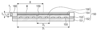
도 2는 도 1의 정전 척의 일 예를 보여주는 단면도이다.
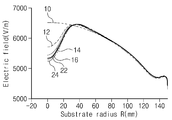
도 3은 도 2의 내부 플레이트의 두께에 따른 상부 플레이트 상의 전기장의 세기를 보여주는 그래프들이다.
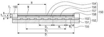
도 4는 도 2의 정전 척의 일 예를 보여주는 단면도이다.
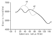
도 5는 도 4의 내부 플레이트, 내부 유전 링, 및 외부 유전 링(의 유전율에 따른 전기장의 세기를 보여주는 그래프들이다.
도 6은 도 1의 정전 척의 일 예를 보여주는 단면도이다.
도 7은 도 6의 내부 플레이트와 내부 유전 링 사이의 제 1 거리에 따른 전기장의 세기를 보여주는 그래프이다.
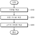
도 8은 도 1의 플라즈마 처리 장치를 이용한 반도체 소자의 제조방법을 보여주는 플로우 챠트이다.
Claims (20)
- 척 베이스;
상기 척 베이스 상에 배치되는 상부 플레이트; 및
상기 척 베이스와 상기 상부 플레이트 사이에 배치되고, 상기 상부 플레이트의 직경보다 작은 직경을 갖는 내부 플레이트를 포함하는 정전 척.
- 제 1 항에 있어서,
상기 내부 플레이트는 상기 상부 플레이트의 유전율보다 작은 유전율을 갖는 정전 척.
- 제 2 항에 있어서,
상기 내부 플레이트는 테프론을 포함하는 정전 척.
- 제 2 항에 있어서,
상기 내부 플레이트를 둘러싸고, 상기 상부 플레이트의 직경과 동일한 외경을 갖는 외부 유전 링을 더 포함하는 정전 척.
- 제 4 항에 있어서,
상기 외부 유전 링은 상기 내부 플레이트의 유전율보다 큰 유전율을 갖는 정정 척.
- 제 4 항에 있어서,
상기 외부 유전 링은 퀄츠를 포함하는 정전 척.
- 제 4 항에 있어서,
상기 외부 유전 링과 상기 내부 플레이트 사이에 배치되는 내부 유전 링을 더 포함하는 정전 척.
- 제 7 항에 있어서,
상기 내부 유전 링은 상기 외부 유전 링의 유전율보다는 작고, 상기 내부 플레이트의 유전율보다는 큰 유전율을 갖는 정전 척.
- 제 7 항에 있어서,
상기 내부 유전 링은 피크, 셀라졸, 또는 마일라를 포함하는 정전 척.
- 제 1 항에 있어서,
상기 내부 플레이트는 상기 상부 플레이트의 두께의 1배 내지 3배의 두께를 갖는 정전 척.
- 제 10 항에 있어서,
상기 내부 플레이트의 두께는 20mm 이하인 정전 척.
- 제 11 항에 있어서,
상기 내부 플레이트의 두께는 1.7mm 내지 5mm인 정전 척.
- 제 1 항에 있어서,
상기 내부 플레이트는 40mm 내지 80mm의 직경을 갖는 플라즈마 처리 장치.
- 제 1 항에 있어서,
상기 척 베이스는:
제 1 하부 플레이트; 및
상기 제 1 하부 플레이트 상에 배치되는 제 2 하부 플레이트를 포함하되,
상기 내부 플레이트는 상기 제 2 하부 플레이트의 상부 면에 제공된 리세스 내에 배치되는 정전 척.
- 제 14 항에 있어서,
상기 리세스는 상기 제 2 하부 플레이트의 중앙에 배치되는 정전 척.
- 챔버;
상기 챔버 내에 배치되어 기판을 수납하는 정전 척; 및
상기 정전 척을 둘러싸는 에지 링을 포함하되,
상기 정전 척은:
척 베이스;
상기 척 베이스 상에 배치되는 상부 플레이트; 및
상기 척 베이스와 상기 상부 플레이트 사이에 배치되고, 상기 상부 플레이트의 직경보다 작은 직경을 갖는 내부 플레이트를 포함하는 플라즈마 처리 장치.
- 제 16 항에 있어서,
상기 척 베이스의 에지 상에 배치되고, 상기 상부 플레이트의 외곽을 둘러싸는 에지 링을 더 포함하되,
상기 내부 플레이트는 상기 에지 링 내에 배치되고, 상기 에지 링보다 얇은 플라즈마 처리 장치.
- 제 17 항에 있어서,
상기 정전 척은 상기 에지 링 내에 배치되고, 상기 내부 플레이트를 둘러싸는 외부 유전 링을 더 포함하는 플라즈마 처리 장치.
- 제 18 항에 있어서,
상기 정전 척은 상기 에지 링 내에 배치되고, 상기 내부 플레이트와 상기 외부 유전 링 사이에 배치되는 내부 유전 링을 더 포함하는 플라즈마 처리 장치.
- 제 19 항에 있어서,
상기 내부 유전 링은 상기 내부 플레이트와 10mm이하의 거리 내에 이격하는 플라즈마 처리 장치.
Priority Applications (3)
| Application Number | Priority Date | Filing Date | Title |
|---|---|---|---|
| KR1020180144455A KR102656790B1 (ko) | 2018-11-21 | 2018-11-21 | 정전 척, 및 그를 포함하는 플라즈마 처리 장치 |
| US16/456,757 US11398397B2 (en) | 2018-11-21 | 2019-06-28 | Electrostatic chuck and plasma processing apparatus including the same |
| CN201910677365.0A CN111211080B (zh) | 2018-11-21 | 2019-07-25 | 静电吸盘和包括该静电吸盘的等离子体处理装置 |
Applications Claiming Priority (1)
| Application Number | Priority Date | Filing Date | Title |
|---|---|---|---|
| KR1020180144455A KR102656790B1 (ko) | 2018-11-21 | 2018-11-21 | 정전 척, 및 그를 포함하는 플라즈마 처리 장치 |
Publications (2)
| Publication Number | Publication Date |
|---|---|
| KR20200059570A true KR20200059570A (ko) | 2020-05-29 |
| KR102656790B1 KR102656790B1 (ko) | 2024-04-12 |
Family
ID=70727114
Family Applications (1)
| Application Number | Title | Priority Date | Filing Date |
|---|---|---|---|
| KR1020180144455A Active KR102656790B1 (ko) | 2018-11-21 | 2018-11-21 | 정전 척, 및 그를 포함하는 플라즈마 처리 장치 |
Country Status (3)
| Country | Link |
|---|---|
| US (1) | US11398397B2 (ko) |
| KR (1) | KR102656790B1 (ko) |
| CN (1) | CN111211080B (ko) |
Cited By (2)
| Publication number | Priority date | Publication date | Assignee | Title |
|---|---|---|---|---|
| KR102576740B1 (ko) | 2023-05-02 | 2023-09-11 | 주식회사 두리머트리얼즈 | 플라즈마 처리장치를 위한 c링 어셈블리 |
| KR102655747B1 (ko) | 2023-04-06 | 2024-04-08 | 주식회사 두리머트리얼즈 | 플라즈마 처리장치를 위한 플레이트 고정장치 |
Families Citing this family (2)
| Publication number | Priority date | Publication date | Assignee | Title |
|---|---|---|---|---|
| KR102841826B1 (ko) | 2020-12-16 | 2025-08-04 | 삼성전자주식회사 | 플라즈마 프로세싱을 위한 정전 척을 포함하는 반도체 공정 설비 |
| CN116110840A (zh) * | 2021-11-09 | 2023-05-12 | 中微半导体设备(上海)股份有限公司 | 提高刻蚀均匀性的静电吸盘、等离子体反应装置 |
Citations (4)
| Publication number | Priority date | Publication date | Assignee | Title |
|---|---|---|---|---|
| JPH07211705A (ja) * | 1994-01-13 | 1995-08-11 | Internatl Business Mach Corp <Ibm> | プラズマの不均一性を制御する装置およびプラズマ生成方法 |
| JP2000323558A (ja) * | 1999-05-07 | 2000-11-24 | Nikon Corp | 静電吸着装置 |
| KR20080014671A (ko) * | 2006-08-10 | 2008-02-14 | 동경 엘렉트론 주식회사 | 플라즈마 처리 장치용 탑재대 및 플라즈마 처리 장치 |
| KR20080070643A (ko) * | 2005-09-30 | 2008-07-30 | 램 리써치 코포레이션 | 유전체 및/또는 상이한 두께, 프로파일 및/또는 형상을갖는 공동을 갖는 정전 척 어셈블리, 그 사용 방법 및그것을 포함한 장치 |
Family Cites Families (15)
| Publication number | Priority date | Publication date | Assignee | Title |
|---|---|---|---|---|
| JP4472372B2 (ja) | 2003-02-03 | 2010-06-02 | 株式会社オクテック | プラズマ処理装置及びプラズマ処理装置用の電極板 |
| US20040261946A1 (en) * | 2003-04-24 | 2004-12-30 | Tokyo Electron Limited | Plasma processing apparatus, focus ring, and susceptor |
| JP4855177B2 (ja) * | 2006-08-10 | 2012-01-18 | 住友大阪セメント株式会社 | 静電チャック装置 |
| US8741098B2 (en) | 2006-08-10 | 2014-06-03 | Tokyo Electron Limited | Table for use in plasma processing system and plasma processing system |
| US8284538B2 (en) | 2006-08-10 | 2012-10-09 | Tokyo Electron Limited | Electrostatic chuck device |
| US20080073032A1 (en) | 2006-08-10 | 2008-03-27 | Akira Koshiishi | Stage for plasma processing apparatus, and plasma processing apparatus |
| JP5029089B2 (ja) | 2007-03-26 | 2012-09-19 | 東京エレクトロン株式会社 | プラズマ処理装置用の載置台及びプラズマ処理装置 |
| US7667944B2 (en) * | 2007-06-29 | 2010-02-23 | Praxair Technology, Inc. | Polyceramic e-chuck |
| JP4898718B2 (ja) | 2008-02-08 | 2012-03-21 | 東京エレクトロン株式会社 | 載置台及びプラズマ処理装置 |
| JP5142914B2 (ja) | 2008-09-25 | 2013-02-13 | 東京エレクトロン株式会社 | 載置台及びプラズマ処理装置 |
| JP2010080717A (ja) | 2008-09-26 | 2010-04-08 | Tokyo Electron Ltd | プラズマ処理装置用の載置台 |
| CN103227083B (zh) * | 2012-01-31 | 2015-08-12 | 中微半导体设备(上海)有限公司 | 一种用于等离子体处理装置的载片台 |
| CN105552014B (zh) * | 2014-10-28 | 2018-09-18 | 北京北方华创微电子装备有限公司 | 一种支撑装置以及等离子刻蚀设备 |
| JP6226092B2 (ja) * | 2016-03-14 | 2017-11-08 | Toto株式会社 | 静電チャック |
| KR20180135152A (ko) | 2017-06-09 | 2018-12-20 | 삼성전자주식회사 | 정전 척, 그를 포함하는 플라즈마 처리 장치 및 그를 이용한 반도체 소자의 제조방법 |
-
2018
- 2018-11-21 KR KR1020180144455A patent/KR102656790B1/ko active Active
-
2019
- 2019-06-28 US US16/456,757 patent/US11398397B2/en active Active
- 2019-07-25 CN CN201910677365.0A patent/CN111211080B/zh active Active
Patent Citations (4)
| Publication number | Priority date | Publication date | Assignee | Title |
|---|---|---|---|---|
| JPH07211705A (ja) * | 1994-01-13 | 1995-08-11 | Internatl Business Mach Corp <Ibm> | プラズマの不均一性を制御する装置およびプラズマ生成方法 |
| JP2000323558A (ja) * | 1999-05-07 | 2000-11-24 | Nikon Corp | 静電吸着装置 |
| KR20080070643A (ko) * | 2005-09-30 | 2008-07-30 | 램 리써치 코포레이션 | 유전체 및/또는 상이한 두께, 프로파일 및/또는 형상을갖는 공동을 갖는 정전 척 어셈블리, 그 사용 방법 및그것을 포함한 장치 |
| KR20080014671A (ko) * | 2006-08-10 | 2008-02-14 | 동경 엘렉트론 주식회사 | 플라즈마 처리 장치용 탑재대 및 플라즈마 처리 장치 |
Cited By (2)
| Publication number | Priority date | Publication date | Assignee | Title |
|---|---|---|---|---|
| KR102655747B1 (ko) | 2023-04-06 | 2024-04-08 | 주식회사 두리머트리얼즈 | 플라즈마 처리장치를 위한 플레이트 고정장치 |
| KR102576740B1 (ko) | 2023-05-02 | 2023-09-11 | 주식회사 두리머트리얼즈 | 플라즈마 처리장치를 위한 c링 어셈블리 |
Also Published As
| Publication number | Publication date |
|---|---|
| KR102656790B1 (ko) | 2024-04-12 |
| US20200161157A1 (en) | 2020-05-21 |
| CN111211080A (zh) | 2020-05-29 |
| US11398397B2 (en) | 2022-07-26 |
| CN111211080B (zh) | 2024-05-07 |
Similar Documents
| Publication | Publication Date | Title |
|---|---|---|
| KR102549546B1 (ko) | 플라즈마 프로세싱 챔버 내의 엘라스토머 시일의 수명을 연장시키는 크기로 형성된 에지 링 | |
| JP7630563B2 (ja) | エッジリングの温度及びバイアスの制御 | |
| KR101008863B1 (ko) | 기판상의 중합체 증착을 감소시키기 위한 디바이스를 구비한 플라즈마 장치 및 중합체 증착을 감소시키는 방법 | |
| KR101342319B1 (ko) | 플라즈마 에칭 챔버를 위한 통합된 용량성 전원과 유도성 전원 | |
| JP5073097B2 (ja) | 電極アセンブリ、基板を処理するための装置および基板を処理するための方法 | |
| US20090206058A1 (en) | Plasma processing apparatus and method, and storage medium | |
| CN111261511B (zh) | 等离子体处理装置和等离子体处理方法 | |
| KR102656790B1 (ko) | 정전 척, 및 그를 포함하는 플라즈마 처리 장치 | |
| KR100735937B1 (ko) | 기판 유지 부재 및 기판 처리 장치 | |
| US20170338084A1 (en) | Plasma processing method | |
| JP2013512564A (ja) | 傾斜側壁を備える静電チャック | |
| KR102758748B1 (ko) | 샤워 헤드 어셈블리 및 이를 갖는 플라즈마 처리 장치 | |
| KR20220021514A (ko) | 상부 전극 및 이를 포함하는 기판 처리 장치 | |
| JPWO2002058125A1 (ja) | プラズマ処理装置およびプラズマ処理方法 | |
| CN111627841A (zh) | 新型边缘刻蚀反应装置和边缘刻蚀方法 | |
| CN101002509A (zh) | 等离子处理单元 | |
| KR102650167B1 (ko) | 정전 척 및 그를 포함하는 플라즈마 처리 장치 | |
| CN120153471A (zh) | 用于稳定带框基板处理的金属屏蔽 | |
| KR102932754B1 (ko) | 에지 링 어셈블리를 포함하는 기판 처리 장치 및 이를 이용한 기판 처리 방법 | |
| KR20230092685A (ko) | 포커스 링을 포함하는 기판 처리 장치 | |
| US20250104978A1 (en) | Ring assembly and substrate processing apparatus comprising the same | |
| KR102787323B1 (ko) | 플라즈마 처리 장치 및 플라즈마 처리 방법 | |
| KR20230092672A (ko) | 포커스 링 및 이를 포함하는 기판 처리 장치 | |
| KR20230092684A (ko) | 링 어셈블리 및 이를 포함하는 기판 처리 장치 | |
| KR20260034986A (ko) | 기판 처리 장치 및 기판 처리 방법 |
Legal Events
| Date | Code | Title | Description |
|---|---|---|---|
| PA0109 | Patent application |
St.27 status event code: A-0-1-A10-A12-nap-PA0109 |
|
| PG1501 | Laying open of application |
St.27 status event code: A-1-1-Q10-Q12-nap-PG1501 |
|
| A201 | Request for examination | ||
| PA0201 | Request for examination |
St.27 status event code: A-1-2-D10-D11-exm-PA0201 |
|
| D13-X000 | Search requested |
St.27 status event code: A-1-2-D10-D13-srh-X000 |
|
| D14-X000 | Search report completed |
St.27 status event code: A-1-2-D10-D14-srh-X000 |
|
| E902 | Notification of reason for refusal | ||
| PE0902 | Notice of grounds for rejection |
St.27 status event code: A-1-2-D10-D21-exm-PE0902 |
|
| E13-X000 | Pre-grant limitation requested |
St.27 status event code: A-2-3-E10-E13-lim-X000 |
|
| P11-X000 | Amendment of application requested |
St.27 status event code: A-2-2-P10-P11-nap-X000 |
|
| P13-X000 | Application amended |
St.27 status event code: A-2-2-P10-P13-nap-X000 |
|
| E701 | Decision to grant or registration of patent right | ||
| PE0701 | Decision of registration |
St.27 status event code: A-1-2-D10-D22-exm-PE0701 |
|
| GRNT | Written decision to grant | ||
| PR0701 | Registration of establishment |
St.27 status event code: A-2-4-F10-F11-exm-PR0701 |
|
| PR1002 | Payment of registration fee |
St.27 status event code: A-2-2-U10-U11-oth-PR1002 Fee payment year number: 1 |
|
| PG1601 | Publication of registration |
St.27 status event code: A-4-4-Q10-Q13-nap-PG1601 |
|
| P22-X000 | Classification modified |
St.27 status event code: A-4-4-P10-P22-nap-X000 |
|
| R18 | Changes to party contact information recorded |
Free format text: ST27 STATUS EVENT CODE: A-5-5-R10-R18-OTH-X000 (AS PROVIDED BY THE NATIONAL OFFICE) |
|
| R18-X000 | Changes to party contact information recorded |
St.27 status event code: A-5-5-R10-R18-oth-X000 |
|
| R18 | Changes to party contact information recorded |
Free format text: ST27 STATUS EVENT CODE: A-5-5-R10-R18-OTH-X000 (AS PROVIDED BY THE NATIONAL OFFICE) |
|
| R18-X000 | Changes to party contact information recorded |
St.27 status event code: A-5-5-R10-R18-oth-X000 |
|
| R18 | Changes to party contact information recorded |
Free format text: ST27 STATUS EVENT CODE: A-5-5-R10-R18-OTH-X000 (AS PROVIDED BY THE NATIONAL OFFICE) |
|
| R18-X000 | Changes to party contact information recorded |
St.27 status event code: A-5-5-R10-R18-oth-X000 |