KR20200060261A - 오목부의 매립 방법 - Google Patents
오목부의 매립 방법 Download PDFInfo
- Publication number
- KR20200060261A KR20200060261A KR1020190147307A KR20190147307A KR20200060261A KR 20200060261 A KR20200060261 A KR 20200060261A KR 1020190147307 A KR1020190147307 A KR 1020190147307A KR 20190147307 A KR20190147307 A KR 20190147307A KR 20200060261 A KR20200060261 A KR 20200060261A
- Authority
- KR
- South Korea
- Prior art keywords
- recess
- gas
- film
- semiconductor film
- amorphous semiconductor
- Prior art date
- Legal status (The legal status is an assumption and is not a legal conclusion. Google has not performed a legal analysis and makes no representation as to the accuracy of the status listed.)
- Granted
Links
Images


Classifications
-
- H—ELECTRICITY
- H10—SEMICONDUCTOR DEVICES; ELECTRIC SOLID-STATE DEVICES NOT OTHERWISE PROVIDED FOR
- H10P—GENERIC PROCESSES OR APPARATUS FOR THE MANUFACTURE OR TREATMENT OF DEVICES COVERED BY CLASS H10
- H10P34/00—Irradiation with electromagnetic or particle radiation of wafers, substrates or parts of devices
- H10P34/40—Irradiation with electromagnetic or particle radiation of wafers, substrates or parts of devices with high-energy radiation
- H10P34/42—Irradiation with electromagnetic or particle radiation of wafers, substrates or parts of devices with high-energy radiation with electromagnetic radiation, e.g. laser annealing
-
- H—ELECTRICITY
- H10—SEMICONDUCTOR DEVICES; ELECTRIC SOLID-STATE DEVICES NOT OTHERWISE PROVIDED FOR
- H10W—GENERIC PACKAGES, INTERCONNECTIONS, CONNECTORS OR OTHER CONSTRUCTIONAL DETAILS OF DEVICES COVERED BY CLASS H10
- H10W20/00—Interconnections in chips, wafers or substrates
- H10W20/01—Manufacture or treatment
- H10W20/031—Manufacture or treatment of conductive parts of the interconnections
- H10W20/032—Manufacture or treatment of conductive parts of the interconnections of conductive barrier, adhesion or liner layers
- H10W20/033—Manufacture or treatment of conductive parts of the interconnections of conductive barrier, adhesion or liner layers in openings in dielectrics
-
- H—ELECTRICITY
- H10—SEMICONDUCTOR DEVICES; ELECTRIC SOLID-STATE DEVICES NOT OTHERWISE PROVIDED FOR
- H10P—GENERIC PROCESSES OR APPARATUS FOR THE MANUFACTURE OR TREATMENT OF DEVICES COVERED BY CLASS H10
- H10P14/00—Formation of materials, e.g. in the shape of layers or pillars
- H10P14/20—Formation of materials, e.g. in the shape of layers or pillars of semiconductor materials
- H10P14/38—Formation of materials, e.g. in the shape of layers or pillars of semiconductor materials characterised by treatments done after the formation of the materials
-
- H01L21/2636—
-
- H01L21/02532—
-
- H01L21/02592—
-
- H01L21/3205—
-
- H01L21/324—
-
- H—ELECTRICITY
- H10—SEMICONDUCTOR DEVICES; ELECTRIC SOLID-STATE DEVICES NOT OTHERWISE PROVIDED FOR
- H10P—GENERIC PROCESSES OR APPARATUS FOR THE MANUFACTURE OR TREATMENT OF DEVICES COVERED BY CLASS H10
- H10P14/00—Formation of materials, e.g. in the shape of layers or pillars
- H10P14/20—Formation of materials, e.g. in the shape of layers or pillars of semiconductor materials
- H10P14/29—Formation of materials, e.g. in the shape of layers or pillars of semiconductor materials characterised by the substrates
- H10P14/2901—Materials
- H10P14/2902—Materials being Group IVA materials
- H10P14/2905—Silicon, silicon germanium or germanium
-
- H—ELECTRICITY
- H10—SEMICONDUCTOR DEVICES; ELECTRIC SOLID-STATE DEVICES NOT OTHERWISE PROVIDED FOR
- H10P—GENERIC PROCESSES OR APPARATUS FOR THE MANUFACTURE OR TREATMENT OF DEVICES COVERED BY CLASS H10
- H10P14/00—Formation of materials, e.g. in the shape of layers or pillars
- H10P14/20—Formation of materials, e.g. in the shape of layers or pillars of semiconductor materials
- H10P14/32—Formation of materials, e.g. in the shape of layers or pillars of semiconductor materials characterised by intermediate layers between substrates and deposited layers
- H10P14/3202—Materials thereof
- H10P14/3238—Materials thereof being insulating materials
-
- H—ELECTRICITY
- H10—SEMICONDUCTOR DEVICES; ELECTRIC SOLID-STATE DEVICES NOT OTHERWISE PROVIDED FOR
- H10P—GENERIC PROCESSES OR APPARATUS FOR THE MANUFACTURE OR TREATMENT OF DEVICES COVERED BY CLASS H10
- H10P14/00—Formation of materials, e.g. in the shape of layers or pillars
- H10P14/20—Formation of materials, e.g. in the shape of layers or pillars of semiconductor materials
- H10P14/32—Formation of materials, e.g. in the shape of layers or pillars of semiconductor materials characterised by intermediate layers between substrates and deposited layers
- H10P14/3242—Structure
-
- H—ELECTRICITY
- H10—SEMICONDUCTOR DEVICES; ELECTRIC SOLID-STATE DEVICES NOT OTHERWISE PROVIDED FOR
- H10P—GENERIC PROCESSES OR APPARATUS FOR THE MANUFACTURE OR TREATMENT OF DEVICES COVERED BY CLASS H10
- H10P14/00—Formation of materials, e.g. in the shape of layers or pillars
- H10P14/20—Formation of materials, e.g. in the shape of layers or pillars of semiconductor materials
- H10P14/34—Deposited materials, e.g. layers
- H10P14/3402—Deposited materials, e.g. layers characterised by the chemical composition
- H10P14/3404—Deposited materials, e.g. layers characterised by the chemical composition being Group IVA materials
- H10P14/3411—Silicon, silicon germanium or germanium
-
- H—ELECTRICITY
- H10—SEMICONDUCTOR DEVICES; ELECTRIC SOLID-STATE DEVICES NOT OTHERWISE PROVIDED FOR
- H10P—GENERIC PROCESSES OR APPARATUS FOR THE MANUFACTURE OR TREATMENT OF DEVICES COVERED BY CLASS H10
- H10P14/00—Formation of materials, e.g. in the shape of layers or pillars
- H10P14/20—Formation of materials, e.g. in the shape of layers or pillars of semiconductor materials
- H10P14/34—Deposited materials, e.g. layers
- H10P14/3451—Structure
- H10P14/3452—Microstructure
- H10P14/3454—Amorphous
-
- H—ELECTRICITY
- H10—SEMICONDUCTOR DEVICES; ELECTRIC SOLID-STATE DEVICES NOT OTHERWISE PROVIDED FOR
- H10P—GENERIC PROCESSES OR APPARATUS FOR THE MANUFACTURE OR TREATMENT OF DEVICES COVERED BY CLASS H10
- H10P14/00—Formation of materials, e.g. in the shape of layers or pillars
- H10P14/40—Formation of materials, e.g. in the shape of layers or pillars of conductive or resistive materials
- H10P14/416—Formation of materials, e.g. in the shape of layers or pillars of conductive or resistive materials of highly doped semiconductor materials, e.g. polysilicon layers or amorphous silicon layers
-
- H—ELECTRICITY
- H10—SEMICONDUCTOR DEVICES; ELECTRIC SOLID-STATE DEVICES NOT OTHERWISE PROVIDED FOR
- H10P—GENERIC PROCESSES OR APPARATUS FOR THE MANUFACTURE OR TREATMENT OF DEVICES COVERED BY CLASS H10
- H10P34/00—Irradiation with electromagnetic or particle radiation of wafers, substrates or parts of devices
- H10P34/40—Irradiation with electromagnetic or particle radiation of wafers, substrates or parts of devices with high-energy radiation
-
- H—ELECTRICITY
- H10—SEMICONDUCTOR DEVICES; ELECTRIC SOLID-STATE DEVICES NOT OTHERWISE PROVIDED FOR
- H10P—GENERIC PROCESSES OR APPARATUS FOR THE MANUFACTURE OR TREATMENT OF DEVICES COVERED BY CLASS H10
- H10P95/00—Generic processes or apparatus for manufacture or treatments not covered by the other groups of this subclass
- H10P95/90—Thermal treatments, e.g. annealing or sintering
-
- H—ELECTRICITY
- H10—SEMICONDUCTOR DEVICES; ELECTRIC SOLID-STATE DEVICES NOT OTHERWISE PROVIDED FOR
- H10W—GENERIC PACKAGES, INTERCONNECTIONS, CONNECTORS OR OTHER CONSTRUCTIONAL DETAILS OF DEVICES COVERED BY CLASS H10
- H10W20/00—Interconnections in chips, wafers or substrates
- H10W20/01—Manufacture or treatment
- H10W20/031—Manufacture or treatment of conductive parts of the interconnections
- H10W20/032—Manufacture or treatment of conductive parts of the interconnections of conductive barrier, adhesion or liner layers
- H10W20/052—Manufacture or treatment of conductive parts of the interconnections of conductive barrier, adhesion or liner layers by treatments not introducing additional elements therein
- H10W20/0526—Manufacture or treatment of conductive parts of the interconnections of conductive barrier, adhesion or liner layers by treatments not introducing additional elements therein by thermal treatment thereof
-
- H—ELECTRICITY
- H10—SEMICONDUCTOR DEVICES; ELECTRIC SOLID-STATE DEVICES NOT OTHERWISE PROVIDED FOR
- H10P—GENERIC PROCESSES OR APPARATUS FOR THE MANUFACTURE OR TREATMENT OF DEVICES COVERED BY CLASS H10
- H10P14/00—Formation of materials, e.g. in the shape of layers or pillars
- H10P14/20—Formation of materials, e.g. in the shape of layers or pillars of semiconductor materials
- H10P14/38—Formation of materials, e.g. in the shape of layers or pillars of semiconductor materials characterised by treatments done after the formation of the materials
- H10P14/3802—Crystallisation or recrystallisation of non-monocrystalline semiconductor materials, e.g. regrowth
- H10P14/3808—Crystallisation or recrystallisation of non-monocrystalline semiconductor materials, e.g. regrowth using laser beams
Landscapes
- Recrystallisation Techniques (AREA)
- Physics & Mathematics (AREA)
- Electromagnetism (AREA)
- Optics & Photonics (AREA)
- Electrodes Of Semiconductors (AREA)
Abstract
본 개시의 일 형태에 의한 오목부의 매립 방법은, 오목부 내에 매립된 아몰퍼스 반도체막에 레이저광을 조사함으로써, 상기 아몰퍼스 반도체막을 결정화시키지 않고 가열하는 가열 공정을 갖는다.
Description
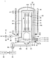
도 2는 종형 열처리 장치의 구성예를 나타내는 종단면도.
도 3은 도 2의 종형 열처리 장치의 반응관을 설명하기 위한 도면.
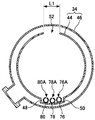
도 4는 레이저 어닐 장치의 구성예를 나타내는 개략도.
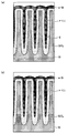
도 5는 레이저 어닐 처리 전후의 결과의 일례를 나타내는 도면.
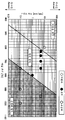
도 6은 레이저 어닐 처리에 있어서 온도와 스위프 속도를 변화시켰을 때의 심(seam)의 개선 효과의 설명도
Claims (8)
- 오목부 내에 매립된 아몰퍼스 반도체막에 레이저광을 조사함으로써, 상기 아몰퍼스 반도체막을 결정화시키지 않고 가열하는 공정을 포함하는,
오목부의 매립 방법. - 제1항에 있어서, 상기 오목부 내에 상기 아몰퍼스 반도체막을 성막하는 공정과, 상기 아몰퍼스 반도체막의 일부를 에칭하는 공정을 반복함으로써, 상기 오목부 내에 상기 아몰퍼스 반도체막을 매립하는 공정을 포함하는,
오목부의 매립 방법. - 제2항에 있어서, 상기 매립하는 공정에서는, 상기 오목부의 개구가 폐색되도록 상기 아몰퍼스 반도체막을 형성하는,
오목부의 매립 방법. - 제1항 내지 제3항 중 어느 한 항에 있어서, 상기 가열하는 공정에서는, 상기 오목부에 대한 상기 레이저광의 조사 위치를 이동시키면서 상기 레이저광을 조사하는,
오목부의 매립 방법. - 제1항 내지 제3항 중 어느 한 항에 있어서, 상기 가열하는 공정에서는, 상기 레이저광의 조사 위치를 고정하여 상기 오목부를 이동시키면서 상기 레이저광을 조사하는,
오목부의 매립 방법. - 제1항 내지 제5항 중 어느 한 항에 있어서, 상기 아몰퍼스 반도체막이 매립된 상기 오목부 내에는 심이 형성되어 있는,
오목부의 매립 방법. - 제1항 내지 제6항 중 어느 한 항에 있어서, 상기 가열하는 공정에서는, 상기 아몰퍼스 반도체막의 막종에 따라, 상기 아몰퍼스 반도체막을 가열하는 온도 및 상기 아몰퍼스 반도체막에 대한 상기 레이저광의 조사 위치의 이동 속도를 조정하는,
오목부의 매립 방법. - 제1항 내지 제7항 중 어느 한 항에 있어서, 상기 아몰퍼스 반도체막은, 아몰퍼스 실리콘막, 아몰퍼스 실리콘 게르마늄막, 또는 아몰퍼스 게르마늄막인,
오목부의 매립 방법.
Applications Claiming Priority (2)
| Application Number | Priority Date | Filing Date | Title |
|---|---|---|---|
| JPJP-P-2018-218602 | 2018-11-21 | ||
| JP2018218602A JP7262210B2 (ja) | 2018-11-21 | 2018-11-21 | 凹部の埋め込み方法 |
Publications (2)
| Publication Number | Publication Date |
|---|---|
| KR20200060261A true KR20200060261A (ko) | 2020-05-29 |
| KR102547550B1 KR102547550B1 (ko) | 2023-06-26 |
Family
ID=70728158
Family Applications (1)
| Application Number | Title | Priority Date | Filing Date |
|---|---|---|---|
| KR1020190147307A Active KR102547550B1 (ko) | 2018-11-21 | 2019-11-18 | 오목부의 매립 방법 |
Country Status (4)
| Country | Link |
|---|---|
| US (1) | US11177133B2 (ko) |
| JP (1) | JP7262210B2 (ko) |
| KR (1) | KR102547550B1 (ko) |
| CN (1) | CN111211093A (ko) |
Citations (4)
| Publication number | Priority date | Publication date | Assignee | Title |
|---|---|---|---|---|
| JPH05275369A (ja) | 1992-03-26 | 1993-10-22 | Toshiba Corp | 半導体装置の製造方法 |
| JP2010251523A (ja) * | 2009-04-15 | 2010-11-04 | Sumco Corp | 部分soiウェーハの製造方法 |
| JP2014194962A (ja) * | 2013-03-28 | 2014-10-09 | Tokyo Electron Ltd | 照射制御方法及び照射制御装置 |
| JP2017183508A (ja) * | 2016-03-30 | 2017-10-05 | 東京エレクトロン株式会社 | シリコン膜の形成方法および形成装置 |
Family Cites Families (32)
| Publication number | Priority date | Publication date | Assignee | Title |
|---|---|---|---|---|
| TW371776B (en) * | 1995-10-15 | 1999-10-11 | Semiconductor Energy Lab Co Ltd | Laser irradiation apparatus and method |
| JP3917698B2 (ja) * | 1996-12-12 | 2007-05-23 | 株式会社半導体エネルギー研究所 | レーザーアニール方法およびレーザーアニール装置 |
| JP3801730B2 (ja) * | 1997-05-09 | 2006-07-26 | 株式会社半導体エネルギー研究所 | プラズマcvd装置及びそれを用いた薄膜形成方法 |
| JP2000183357A (ja) * | 1998-12-21 | 2000-06-30 | Matsushita Electric Ind Co Ltd | 薄膜トランジスタ及びその製造方法 |
| JP2000223549A (ja) * | 1999-01-29 | 2000-08-11 | Canon Inc | 基板搬送装置、基板搬送方法、基板搬送用ハンド機構、灰化処理装置及び灰化処理方法 |
| US7098084B2 (en) * | 2000-03-08 | 2006-08-29 | Semiconductor Energy Laboratory Co., Ltd. | Semiconductor device and manufacturing method thereof |
| KR20020019419A (ko) * | 2000-09-05 | 2002-03-12 | 이데이 노부유끼 | 박막 제조 방법, 반도체 박막, 반도체 디바이스, 반도체박막 제조 방법, 및 반도체 박막 제조 장치 |
| US6816330B2 (en) * | 2000-12-22 | 2004-11-09 | Matsushita Electric Industrial Co., Ltd. | Method for forming a magnetic pattern in a magnetic recording medium, magnetic recording medium magnetic recording device and photomask |
| US7214573B2 (en) * | 2001-12-11 | 2007-05-08 | Semiconductor Energy Laboratory Co., Ltd. | Method of manufacturing a semiconductor device that includes patterning sub-islands |
| US7749818B2 (en) * | 2002-01-28 | 2010-07-06 | Semiconductor Energy Laboratory Co., Ltd. | Semiconductor device and method of manufacturing the same |
| TWI261358B (en) * | 2002-01-28 | 2006-09-01 | Semiconductor Energy Lab | Semiconductor device and method of manufacturing the same |
| US6841434B2 (en) * | 2002-03-26 | 2005-01-11 | Semiconductor Energy Laboratory Co., Ltd. | Method of fabricating semiconductor device |
| TW200541079A (en) * | 2004-06-04 | 2005-12-16 | Adv Lcd Tech Dev Ct Co Ltd | Crystallizing method, thin-film transistor manufacturing method, thin-film transistor, and display device |
| US20060202269A1 (en) * | 2005-03-08 | 2006-09-14 | Semiconductor Energy Laboratory Co., Ltd. | Wireless chip and electronic appliance having the same |
| KR101162557B1 (ko) * | 2005-03-15 | 2012-07-05 | 가부시키가이샤 한도오따이 에네루기 켄큐쇼 | 반도체 장치 및 이를 갖는 전자 장치 |
| US20060260545A1 (en) * | 2005-05-17 | 2006-11-23 | Kartik Ramaswamy | Low temperature absorption layer deposition and high speed optical annealing system |
| JP2007227837A (ja) | 2006-02-27 | 2007-09-06 | Seiko Epson Corp | 半導体装置の製造方法及び半導体装置、電気光学装置、並びに電子機器 |
| JP5100048B2 (ja) | 2006-07-06 | 2012-12-19 | 住友重機械工業株式会社 | 結晶化半導体膜の製造方法 |
| JP5053610B2 (ja) * | 2006-09-29 | 2012-10-17 | 富士フイルム株式会社 | レーザアニール方法、半導体膜、半導体装置、及び電気光学装置 |
| US20100193792A1 (en) * | 2007-07-20 | 2010-08-05 | Toshiaki Miyajima | Laminated film manufacturing method, semiconductor device manufacturing method, semiconductor device and display device |
| US7943414B2 (en) * | 2008-08-01 | 2011-05-17 | Semiconductor Energy Laboratory Co., Ltd. | Method for manufacturing SOI substrate |
| JP5564879B2 (ja) * | 2009-10-01 | 2014-08-06 | 三菱電機株式会社 | 非晶質半導体膜の結晶化方法、並びに薄膜トランジスタ、半導体装置、表示装置、及びその製造方法 |
| JP4678700B1 (ja) * | 2009-11-30 | 2011-04-27 | 株式会社日本製鋼所 | レーザアニール装置およびレーザアニール方法 |
| JP2012015445A (ja) * | 2010-07-05 | 2012-01-19 | Japan Steel Works Ltd:The | レーザアニール処理装置およびレーザアニール処理方法 |
| US8518808B2 (en) * | 2010-09-17 | 2013-08-27 | The United States Of America, As Represented By The Secretary Of The Navy | Defects annealing and impurities activation in III-nitride compound |
| JP5641965B2 (ja) | 2011-02-09 | 2014-12-17 | 住友重機械工業株式会社 | レーザアニール方法及びレーザアニール装置 |
| JP6423135B2 (ja) * | 2012-11-29 | 2018-11-14 | 三星ダイヤモンド工業株式会社 | パターン付き基板の分割方法 |
| US9543168B2 (en) * | 2015-02-06 | 2017-01-10 | The United States Of America, As Represented By The Secretary Of The Navy | Defects annealing and impurities activation in semiconductors at thermodynamically non-stable conditions |
| JP6615658B2 (ja) * | 2016-03-16 | 2019-12-04 | 株式会社ブイ・テクノロジー | マスク及び薄膜トランジスタの製造方法 |
| JP2018037628A (ja) | 2016-08-31 | 2018-03-08 | 国立大学法人島根大学 | パターニング方法、薄膜トランジスタ作製方法、および、パターニング装置 |
| US10008418B2 (en) * | 2016-09-30 | 2018-06-26 | Taiwan Semiconductor Manufacturing Co., Ltd. | Method of semiconductor integrated circuit fabrication |
| WO2019213001A1 (en) * | 2018-05-04 | 2019-11-07 | The Government Of The United States Of America, As Represented By The Secretary Of The Navy | Implanted dopant activation for wide bandgap semiconductor electronics |
-
2018
- 2018-11-21 JP JP2018218602A patent/JP7262210B2/ja active Active
-
2019
- 2019-11-18 KR KR1020190147307A patent/KR102547550B1/ko active Active
- 2019-11-18 CN CN201911127515.7A patent/CN111211093A/zh active Pending
- 2019-11-21 US US16/690,958 patent/US11177133B2/en active Active
Patent Citations (4)
| Publication number | Priority date | Publication date | Assignee | Title |
|---|---|---|---|---|
| JPH05275369A (ja) | 1992-03-26 | 1993-10-22 | Toshiba Corp | 半導体装置の製造方法 |
| JP2010251523A (ja) * | 2009-04-15 | 2010-11-04 | Sumco Corp | 部分soiウェーハの製造方法 |
| JP2014194962A (ja) * | 2013-03-28 | 2014-10-09 | Tokyo Electron Ltd | 照射制御方法及び照射制御装置 |
| JP2017183508A (ja) * | 2016-03-30 | 2017-10-05 | 東京エレクトロン株式会社 | シリコン膜の形成方法および形成装置 |
Also Published As
| Publication number | Publication date |
|---|---|
| KR102547550B1 (ko) | 2023-06-26 |
| US20200161135A1 (en) | 2020-05-21 |
| JP2020088106A (ja) | 2020-06-04 |
| CN111211093A (zh) | 2020-05-29 |
| US11177133B2 (en) | 2021-11-16 |
| JP7262210B2 (ja) | 2023-04-21 |
Similar Documents
| Publication | Publication Date | Title |
|---|---|---|
| KR102158406B1 (ko) | 실리콘막의 형성 방법 및 형성 장치, 및 기억 매체 | |
| KR102639767B1 (ko) | 폴리실리콘막의 형성 방법 및 성막 장치 | |
| TW202205361A (zh) | 半導體材料的選擇性精準蝕刻 | |
| US10262872B2 (en) | Method of manufacturing semiconductor device, substrate processing apparatus, and recording medium | |
| US10090152B2 (en) | Method of manufacturing semiconductor device, substrate processing apparatus, and recording medium | |
| US20120260857A1 (en) | Heat treatment apparatus | |
| JP6640596B2 (ja) | 成膜方法 | |
| TWI710669B (zh) | 半導體裝置之製造方法及半導體製造裝置 | |
| KR102441233B1 (ko) | 반도체 막의 형성 방법 및 성막 장치 | |
| KR20240159934A (ko) | 반도체 재료의 선택적 정밀 에칭 | |
| US11177133B2 (en) | Method of filling recess | |
| TW202331789A (zh) | 整合式磊晶與預清潔系統 | |
| CN111793790B (zh) | 成膜方法和成膜装置 | |
| JP6584348B2 (ja) | 凹部の埋め込み方法および処理装置 | |
| CN110233096B (zh) | 硅膜的成膜方法和基板处理装置 | |
| KR102696238B1 (ko) | 성막 방법 및 열처리 장치 | |
| KR102732069B1 (ko) | 막 형성 방법 및 막 형성 장치 | |
| JP7601503B2 (ja) | 半導体装置の製造方法及び基板処理装置 | |
| KR102651480B1 (ko) | 성막 방법 및 성막 장치 | |
| KR102709049B1 (ko) | 기판 처리 장치 | |
| CN116264158A (zh) | 动态激光辅助蚀刻方法 | |
| KR20260066781A (ko) | 기판 처리 방법 및 기판 처리 장치 |
Legal Events
| Date | Code | Title | Description |
|---|---|---|---|
| PA0109 | Patent application |
St.27 status event code: A-0-1-A10-A12-nap-PA0109 |
|
| PG1501 | Laying open of application |
St.27 status event code: A-1-1-Q10-Q12-nap-PG1501 |
|
| A201 | Request for examination | ||
| PA0201 | Request for examination |
St.27 status event code: A-1-2-D10-D11-exm-PA0201 |
|
| D13-X000 | Search requested |
St.27 status event code: A-1-2-D10-D13-srh-X000 |
|
| D14-X000 | Search report completed |
St.27 status event code: A-1-2-D10-D14-srh-X000 |
|
| E902 | Notification of reason for refusal | ||
| PE0902 | Notice of grounds for rejection |
St.27 status event code: A-1-2-D10-D21-exm-PE0902 |
|
| E13-X000 | Pre-grant limitation requested |
St.27 status event code: A-2-3-E10-E13-lim-X000 |
|
| P11-X000 | Amendment of application requested |
St.27 status event code: A-2-2-P10-P11-nap-X000 |
|
| P13-X000 | Application amended |
St.27 status event code: A-2-2-P10-P13-nap-X000 |
|
| E701 | Decision to grant or registration of patent right | ||
| PE0701 | Decision of registration |
St.27 status event code: A-1-2-D10-D22-exm-PE0701 |
|
| GRNT | Written decision to grant | ||
| PR0701 | Registration of establishment |
St.27 status event code: A-2-4-F10-F11-exm-PR0701 |
|
| PR1002 | Payment of registration fee |
St.27 status event code: A-2-2-U10-U11-oth-PR1002 Fee payment year number: 1 |
|
| PG1601 | Publication of registration |
St.27 status event code: A-4-4-Q10-Q13-nap-PG1601 |
|
| P22-X000 | Classification modified |
St.27 status event code: A-4-4-P10-P22-nap-X000 |
|
| PR1001 | Payment of annual fee |
St.27 status event code: A-4-4-U10-U11-oth-PR1001 Fee payment year number: 4 |
|
| U11 | Full renewal or maintenance fee paid |
Free format text: ST27 STATUS EVENT CODE: A-4-4-U10-U11-OTH-PR1001 (AS PROVIDED BY THE NATIONAL OFFICE) Year of fee payment: 4 |