KR20200062081A - 광학 표시 패널의 손상 검사 방법 - Google Patents
광학 표시 패널의 손상 검사 방법 Download PDFInfo
- Publication number
- KR20200062081A KR20200062081A KR1020197037780A KR20197037780A KR20200062081A KR 20200062081 A KR20200062081 A KR 20200062081A KR 1020197037780 A KR1020197037780 A KR 1020197037780A KR 20197037780 A KR20197037780 A KR 20197037780A KR 20200062081 A KR20200062081 A KR 20200062081A
- Authority
- KR
- South Korea
- Prior art keywords
- panel
- optical display
- display panel
- light
- inspection
- Prior art date
- Legal status (The legal status is an assumption and is not a legal conclusion. Google has not performed a legal analysis and makes no representation as to the accuracy of the status listed.)
- Granted
Links
Images




Classifications
-
- G—PHYSICS
- G01—MEASURING; TESTING
- G01N—INVESTIGATING OR ANALYSING MATERIALS BY DETERMINING THEIR CHEMICAL OR PHYSICAL PROPERTIES
- G01N21/00—Investigating or analysing materials by the use of optical means, i.e. using sub-millimetre waves, infrared, visible or ultraviolet light
- G01N21/84—Systems specially adapted for particular applications
- G01N21/88—Investigating the presence of flaws or contamination
- G01N21/95—Investigating the presence of flaws or contamination characterised by the material or shape of the object to be examined
- G01N21/956—Inspecting patterns on the surface of objects
-
- G—PHYSICS
- G01—MEASURING; TESTING
- G01B—MEASURING LENGTH, THICKNESS OR SIMILAR LINEAR DIMENSIONS; MEASURING ANGLES; MEASURING AREAS; MEASURING IRREGULARITIES OF SURFACES OR CONTOURS
- G01B11/00—Measuring arrangements characterised by the use of optical techniques
- G01B11/30—Measuring arrangements characterised by the use of optical techniques for measuring roughness or irregularity of surfaces
-
- G—PHYSICS
- G01—MEASURING; TESTING
- G01N—INVESTIGATING OR ANALYSING MATERIALS BY DETERMINING THEIR CHEMICAL OR PHYSICAL PROPERTIES
- G01N21/00—Investigating or analysing materials by the use of optical means, i.e. using sub-millimetre waves, infrared, visible or ultraviolet light
- G01N21/84—Systems specially adapted for particular applications
- G01N21/88—Investigating the presence of flaws or contamination
- G01N21/95—Investigating the presence of flaws or contamination characterised by the material or shape of the object to be examined
Landscapes
- Physics & Mathematics (AREA)
- General Physics & Mathematics (AREA)
- General Health & Medical Sciences (AREA)
- Chemical & Material Sciences (AREA)
- Analytical Chemistry (AREA)
- Biochemistry (AREA)
- Life Sciences & Earth Sciences (AREA)
- Health & Medical Sciences (AREA)
- Immunology (AREA)
- Pathology (AREA)
- Investigating Materials By The Use Of Optical Means Adapted For Particular Applications (AREA)
- Length Measuring Devices By Optical Means (AREA)
- Testing Of Optical Devices Or Fibers (AREA)
- Manufacture Of Electron Tubes, Discharge Lamp Vessels, Lead-In Wires, And The Like (AREA)
- Investigating Or Analysing Materials By Optical Means (AREA)
Abstract
Description
도 2는 본 발명의 일실시형태에 의한 검사 방법을 실현하는 검사 장치의 구성의 개요, 배치 위치 및 검사 장치와 광학 표시 패널의 흐름의 관계를 나타낸다.
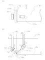
도 3은 본 발명의 일실시형태에 의한 검사 방법을 실현하는 검사 장치의 구성 예를 나타내고, (a)는 광학 표시 패널 및 검사 유닛을 상면으로부터 본 도면이고, (b)는 광학 표시 패널 및 검사 유닛을 측면으로부터 본 도면이다.
도 4는 패널 단부에 광을 조사한 경우의 촬영 화상을 나타내고, (a)는 본 발명의 일실시형태에 의한 검사 방법에 있어서 촬영된 정반사광에 의한 패널 단부의 촬영 화상의 예이고, (b)는 종래의 검사 방법에 있어서의 산란광에 의한 패널 단부의 촬영 화상의 예이다.
도 5는 본 발명의 일실시형태에 의한 검사 방법에 있어서, 취득된 화상으로부터 손상의 유무를 판정하는 방법을 나타내는 플로우도이다.
Pe 패널 단부
Pea, Peb, Pec, Ped 패널 가장자리
P1 광학 필름 접합 완료된 광학 표시 패널
1 광학 필름 접합 장치
10 검사부
11a, 11b, 11c, 11d 검사 유닛
12a, 12b, 12c, 12d 평면형 조명
13a, 13b, 13c, 13d 에어리어 카메라
16a, 16b, 16c 이동용 레일
14a, 14b, 14c, 14d 검사 영역
20 처리·제어부
15 식별 표지
30 패널 투입부
40 세정부
50 접합부
60 가압 탈포부
70 패널 반출부
Claims (6)
- 광학 표시 패널에 있어서의 패널 단부의 손상을 검사하기 위한 검사 방법으로서,
패널 단부를 향해서 조사광을 조사하는 공정과,
조사광이 상기 패널 단부에서 반사됨으로써 생성된 반사광을 수광하는 공정과,
수광된 반사광에 기초하여 취득된 화상에 있어서, 상기 패널 단부에 대응하는 영역과 상기 패널 단부의 배경에 대응하는 영역을 구획하는 윤곽선을 검출하는 공정을 포함하고,
조사광을 조사하는 공정은 상기 취득된 화상에 있어서 상기 패널 단부에 상당하는 영역에 상기 윤곽선 이외의 선이 존재하지 않도록, 상기 패널 단부에 상당하는 영역을 과도 노출시키는데 충분한 강도로 조사광을 조사하는 것을 포함하는 검사 방법. - 제 1 항에 있어서,
반사광은 정반사광인 검사 방법. - 제 2 항에 있어서,
반사광의 휘도가 3000~10000cd/m2인 검사 방법. - 제 1 항 내지 제 3 항 중 어느 한 항에 있어서,
검출되는 손상은 상기 패널 단부에 있어서 일방의 면으로부터 타방의 면까지 미치는 손상인 검사 방법. - 제 1 항 내지 제 3 항 중 어느 한 항에 있어서,
상기 취득된 화상은 상기 패널 단부를 이동시키면서 연속적으로 취득된 복수의 화상이고, 시간적으로 전후하는 2개의 화상은 각각 일부가 겹치도록 촬상된 것인 검사 방법. - 제 1 항 내지 제 3 항 중 어느 한 항에 있어서,
조사광은 평면형 조명으로부터 방사되는 광인 검사 방법.
Applications Claiming Priority (3)
| Application Number | Priority Date | Filing Date | Title |
|---|---|---|---|
| JP2017187930A JP6937647B2 (ja) | 2017-09-28 | 2017-09-28 | 光学表示パネルの損傷検査方法 |
| JPJP-P-2017-187930 | 2017-09-28 | ||
| PCT/JP2018/004177 WO2019064622A1 (ja) | 2017-09-28 | 2018-02-07 | 光学表示パネルの損傷検査方法 |
Publications (2)
| Publication Number | Publication Date |
|---|---|
| KR20200062081A true KR20200062081A (ko) | 2020-06-03 |
| KR102495565B1 KR102495565B1 (ko) | 2023-02-03 |
Family
ID=65903437
Family Applications (1)
| Application Number | Title | Priority Date | Filing Date |
|---|---|---|---|
| KR1020197037780A Active KR102495565B1 (ko) | 2017-09-28 | 2018-02-07 | 광학 표시 패널의 손상 검사 방법 |
Country Status (5)
| Country | Link |
|---|---|
| JP (1) | JP6937647B2 (ko) |
| KR (1) | KR102495565B1 (ko) |
| CN (1) | CN110945347B (ko) |
| TW (1) | TWI779055B (ko) |
| WO (1) | WO2019064622A1 (ko) |
Families Citing this family (1)
| Publication number | Priority date | Publication date | Assignee | Title |
|---|---|---|---|---|
| JP7030914B1 (ja) * | 2020-08-27 | 2022-03-07 | 花王株式会社 | シート状部材の製造方法 |
Citations (6)
| Publication number | Priority date | Publication date | Assignee | Title |
|---|---|---|---|---|
| JP2003247953A (ja) | 2002-02-25 | 2003-09-05 | Seiko Epson Corp | 液晶パネル外観検査方法及び検査装置 |
| KR100418357B1 (ko) * | 2003-03-31 | 2004-02-14 | (주)에이치아이티에스 | 엘시디(lcd) 패널의 측면검사장치 및 방법 |
| WO2004079352A1 (ja) * | 2003-03-04 | 2004-09-16 | Mitsuboshi Diamond Industrial Co. Ltd. | 透明基板端面部の検査装置およびその検査方法 |
| JP2006208259A (ja) * | 2005-01-31 | 2006-08-10 | Aisin Seiki Co Ltd | 欠陥検査方法および欠陥検査装置 |
| JP2011232324A (ja) * | 2010-04-09 | 2011-11-17 | Nippon Steel Corp | 表面欠陥検査装置、表面欠陥検査方法及びプログラム |
| JP2015169564A (ja) * | 2014-03-07 | 2015-09-28 | 株式会社ダイヘン | 画像検査装置及び画像検査方法 |
Family Cites Families (11)
| Publication number | Priority date | Publication date | Assignee | Title |
|---|---|---|---|---|
| JP3025946B2 (ja) * | 1995-10-11 | 2000-03-27 | 茨城県 | 物体表面の粗さ測定方法及び装置 |
| JPH11271035A (ja) * | 1998-03-24 | 1999-10-05 | Hitachi Metals Ltd | 欠陥検査装置及び欠陥検査方法 |
| US6628381B1 (en) * | 2000-06-20 | 2003-09-30 | Applied Materials, Inc. | Optical inspection method and apparatus utilizing a collection angle design |
| JP4703911B2 (ja) * | 2001-08-10 | 2011-06-15 | 日新製鋼株式会社 | 金属帯の孔状欠陥検査装置 |
| WO2004088399A1 (en) * | 2003-03-31 | 2004-10-14 | Hits Co., Ltd. | Lcd cell edge inspection apparatus and method thereof |
| JP4626982B2 (ja) * | 2005-02-10 | 2011-02-09 | セントラル硝子株式会社 | ガラス板の端面の欠陥検出装置および検出方法 |
| JP5015824B2 (ja) * | 2008-02-29 | 2012-08-29 | 日東電工株式会社 | 粘着フィルム位置検出器および粘着フィルム貼付装置 |
| CN102713506B (zh) * | 2009-12-17 | 2014-09-17 | 新日铁住金株式会社 | 管状物的检查装置及其检查方法 |
| JP2011257257A (ja) * | 2010-06-09 | 2011-12-22 | Panasonic Corp | 検査装置、検査方法およびこれらを用いた画像表示用パネルの製造方法 |
| CN204215118U (zh) * | 2014-12-02 | 2015-03-18 | 北京兆维电子(集团)有限责任公司 | 液晶屏外观检测装置 |
| JP6344290B2 (ja) * | 2015-04-01 | 2018-06-20 | 東芝三菱電機産業システム株式会社 | 平面形状測定装置 |
-
2017
- 2017-09-28 JP JP2017187930A patent/JP6937647B2/ja active Active
-
2018
- 2018-02-07 CN CN201880048168.6A patent/CN110945347B/zh active Active
- 2018-02-07 WO PCT/JP2018/004177 patent/WO2019064622A1/ja not_active Ceased
- 2018-02-07 KR KR1020197037780A patent/KR102495565B1/ko active Active
- 2018-06-29 TW TW107122468A patent/TWI779055B/zh active
Patent Citations (6)
| Publication number | Priority date | Publication date | Assignee | Title |
|---|---|---|---|---|
| JP2003247953A (ja) | 2002-02-25 | 2003-09-05 | Seiko Epson Corp | 液晶パネル外観検査方法及び検査装置 |
| WO2004079352A1 (ja) * | 2003-03-04 | 2004-09-16 | Mitsuboshi Diamond Industrial Co. Ltd. | 透明基板端面部の検査装置およびその検査方法 |
| KR100418357B1 (ko) * | 2003-03-31 | 2004-02-14 | (주)에이치아이티에스 | 엘시디(lcd) 패널의 측면검사장치 및 방법 |
| JP2006208259A (ja) * | 2005-01-31 | 2006-08-10 | Aisin Seiki Co Ltd | 欠陥検査方法および欠陥検査装置 |
| JP2011232324A (ja) * | 2010-04-09 | 2011-11-17 | Nippon Steel Corp | 表面欠陥検査装置、表面欠陥検査方法及びプログラム |
| JP2015169564A (ja) * | 2014-03-07 | 2015-09-28 | 株式会社ダイヘン | 画像検査装置及び画像検査方法 |
Also Published As
| Publication number | Publication date |
|---|---|
| WO2019064622A1 (ja) | 2019-04-04 |
| CN110945347B (zh) | 2024-01-12 |
| TWI779055B (zh) | 2022-10-01 |
| JP2019060823A (ja) | 2019-04-18 |
| KR102495565B1 (ko) | 2023-02-03 |
| TW201915481A (zh) | 2019-04-16 |
| CN110945347A (zh) | 2020-03-31 |
| JP6937647B2 (ja) | 2021-09-22 |
Similar Documents
| Publication | Publication Date | Title |
|---|---|---|
| JP5825278B2 (ja) | 欠陥検査装置および欠陥検査方法 | |
| KR101733197B1 (ko) | 멀티 광학 비전 장치 | |
| CN110596130A (zh) | 一种具有辅助照明的工业检测装置 | |
| JP6249338B2 (ja) | 外観検査装置 | |
| TW201623947A (zh) | 透射型缺陷檢查裝置及缺陷檢查方法 | |
| JP5410092B2 (ja) | 複合構造に不整合がないか検査するための装置および方法 | |
| CN111426696B (zh) | 顶覆橡胶片的橡胶附着不良检测装置 | |
| JP2009216628A (ja) | 欠陥検出装置および欠陥検出方法 | |
| JPH11271038A (ja) | 塗装欠陥検査装置 | |
| JP2007147433A (ja) | セラミック板の欠陥検出方法と装置 | |
| KR102162693B1 (ko) | 결함 검출 시스템 및 방법 | |
| KR102495565B1 (ko) | 광학 표시 패널의 손상 검사 방법 | |
| KR20190001789A (ko) | 멀티 광학 디스플레이 검사 장치 | |
| JPH10132754A (ja) | リードフレームの外観検査装置 | |
| KR102528464B1 (ko) | 비전 검사 장치 | |
| KR20210148782A (ko) | 검사 대상물 표면의 결함을 검출하는 결함 검출 장치 | |
| JP2005127747A (ja) | 板材の表面欠陥検査方法および表面欠陥検査装置 | |
| JP4792314B2 (ja) | 基板検査装置および基板検査方法 | |
| JP2006189294A (ja) | ムラ欠陥の検査方法および装置 | |
| JP4815796B2 (ja) | 欠陥検査装置 | |
| JP2000283740A (ja) | 押出成形品の外観検査装置 | |
| JP6358884B2 (ja) | 検査装置 | |
| JP2006064501A (ja) | 中空糸膜の断面形状測定方法および装置 | |
| JPH0224544A (ja) | 瓶の外観検査装置 |
Legal Events
| Date | Code | Title | Description |
|---|---|---|---|
| PA0105 | International application |
Patent event date: 20191220 Patent event code: PA01051R01D Comment text: International Patent Application |
|
| PG1501 | Laying open of application | ||
| PA0201 | Request for examination |
Patent event code: PA02012R01D Patent event date: 20201112 Comment text: Request for Examination of Application |
|
| E902 | Notification of reason for refusal | ||
| PE0902 | Notice of grounds for rejection |
Comment text: Notification of reason for refusal Patent event date: 20220518 Patent event code: PE09021S01D |
|
| E701 | Decision to grant or registration of patent right | ||
| PE0701 | Decision of registration |
Patent event code: PE07011S01D Comment text: Decision to Grant Registration Patent event date: 20221124 |
|
| GRNT | Written decision to grant | ||
| PR0701 | Registration of establishment |
Comment text: Registration of Establishment Patent event date: 20230131 Patent event code: PR07011E01D |
|
| PR1002 | Payment of registration fee |
Payment date: 20230201 End annual number: 3 Start annual number: 1 |
|
| PG1601 | Publication of registration |