KR20200062244A - 집적 회로 패키지에 프로그램 가능 디바이스 및 처리 시스템의 통합 - Google Patents
집적 회로 패키지에 프로그램 가능 디바이스 및 처리 시스템의 통합 Download PDFInfo
- Publication number
- KR20200062244A KR20200062244A KR1020207011292A KR20207011292A KR20200062244A KR 20200062244 A KR20200062244 A KR 20200062244A KR 1020207011292 A KR1020207011292 A KR 1020207011292A KR 20207011292 A KR20207011292 A KR 20207011292A KR 20200062244 A KR20200062244 A KR 20200062244A
- Authority
- KR
- South Korea
- Prior art keywords
- programmable
- interface
- processing system
- package
- coupled
- Prior art date
- Legal status (The legal status is an assumption and is not a legal conclusion. Google has not performed a legal analysis and makes no representation as to the accuracy of the status listed.)
- Granted
Links
Images







Classifications
-
- G—PHYSICS
- G06—COMPUTING OR CALCULATING; COUNTING
- G06F—ELECTRIC DIGITAL DATA PROCESSING
- G06F15/00—Digital computers in general; Data processing equipment in general
- G06F15/76—Architectures of general purpose stored program computers
- G06F15/78—Architectures of general purpose stored program computers comprising a single central processing unit
- G06F15/7807—System on chip, i.e. computer system on a single chip; System in package, i.e. computer system on one or more chips in a single package
-
- H—ELECTRICITY
- H10—SEMICONDUCTOR DEVICES; ELECTRIC SOLID-STATE DEVICES NOT OTHERWISE PROVIDED FOR
- H10W—GENERIC PACKAGES, INTERCONNECTIONS, CONNECTORS OR OTHER CONSTRUCTIONAL DETAILS OF DEVICES COVERED BY CLASS H10
- H10W70/00—Package substrates; Interposers; Redistribution layers [RDL]
- H10W70/60—Insulating or insulated package substrates; Interposers; Redistribution layers
- H10W70/62—Insulating or insulated package substrates; Interposers; Redistribution layers characterised by their interconnections
- H10W70/65—Shapes or dispositions of interconnections
-
- G—PHYSICS
- G06—COMPUTING OR CALCULATING; COUNTING
- G06F—ELECTRIC DIGITAL DATA PROCESSING
- G06F15/00—Digital computers in general; Data processing equipment in general
- G06F15/76—Architectures of general purpose stored program computers
- G06F15/78—Architectures of general purpose stored program computers comprising a single central processing unit
- G06F15/7867—Architectures of general purpose stored program computers comprising a single central processing unit with reconfigurable architecture
- G06F15/7885—Runtime interface, e.g. data exchange, runtime control
- G06F15/7892—Reconfigurable logic embedded in CPU, e.g. reconfigurable unit
-
- G—PHYSICS
- G06—COMPUTING OR CALCULATING; COUNTING
- G06F—ELECTRIC DIGITAL DATA PROCESSING
- G06F13/00—Interconnection of, or transfer of information or other signals between, memories, input/output devices or central processing units
- G06F13/38—Information transfer, e.g. on bus
- G06F13/40—Bus structure
-
- G—PHYSICS
- G06—COMPUTING OR CALCULATING; COUNTING
- G06F—ELECTRIC DIGITAL DATA PROCESSING
- G06F15/00—Digital computers in general; Data processing equipment in general
- G06F15/76—Architectures of general purpose stored program computers
- G06F15/78—Architectures of general purpose stored program computers comprising a single central processing unit
- G06F15/7867—Architectures of general purpose stored program computers comprising a single central processing unit with reconfigurable architecture
-
- H01L23/50—
-
- H01L23/5386—
-
- H—ELECTRICITY
- H10—SEMICONDUCTOR DEVICES; ELECTRIC SOLID-STATE DEVICES NOT OTHERWISE PROVIDED FOR
- H10W—GENERIC PACKAGES, INTERCONNECTIONS, CONNECTORS OR OTHER CONSTRUCTIONAL DETAILS OF DEVICES COVERED BY CLASS H10
- H10W70/00—Package substrates; Interposers; Redistribution layers [RDL]
- H10W70/60—Insulating or insulated package substrates; Interposers; Redistribution layers
- H10W70/611—Insulating or insulated package substrates; Interposers; Redistribution layers for connecting multiple chips together
-
- H—ELECTRICITY
- H10—SEMICONDUCTOR DEVICES; ELECTRIC SOLID-STATE DEVICES NOT OTHERWISE PROVIDED FOR
- H10W—GENERIC PACKAGES, INTERCONNECTIONS, CONNECTORS OR OTHER CONSTRUCTIONAL DETAILS OF DEVICES COVERED BY CLASS H10
- H10W72/00—Interconnections or connectors in packages
Landscapes
- Engineering & Computer Science (AREA)
- Computer Hardware Design (AREA)
- Theoretical Computer Science (AREA)
- General Engineering & Computer Science (AREA)
- Physics & Mathematics (AREA)
- General Physics & Mathematics (AREA)
- Computing Systems (AREA)
- Microelectronics & Electronic Packaging (AREA)
- Logic Circuits (AREA)
- Design And Manufacture Of Integrated Circuits (AREA)
- Semiconductor Integrated Circuits (AREA)
- Geometry (AREA)
- Microcomputers (AREA)
- Multi Processors (AREA)
Abstract
Description
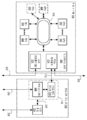
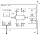
도 1은 일 예에 따른 집적 회로(IC) 패키지를 도시한 블록도이다.
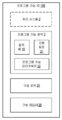
도 2는 도 1의 IC 패키지에서의 처리 시스템 및 프로그램 가능 IC의 예를 도시한 블록도이다.
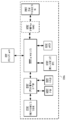
도 3은 일 예에 따른 프로그램 가능 IC의 주변 회로를 도시한 블록도이다.
도 4는 일 예에 따른 도 3의 주변 회로를 보다 상세히 도시한 블록도이다.
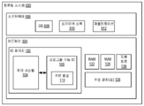
도 5는 일 예에 따른 컴퓨팅 시스템을 도시한 블록도이다.
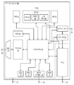
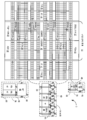
도 6은 일 예에 따른 프로그램 가능 IC를 도시한 블록도이다.
도 7은 일 예에 따른 프로그램 가능 IC의 시스템 온 칩(SoC) 구현을 도시한 블록도이다.
도 8은 프로그램 가능 IC의 필드 프로그램 가능 게이트 어레이(FPGA) 구현을 도시한다.
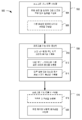
도 9는 일 예에 따른 IC 패키지에서 프로그램 가능 IC를 동작시키는 방법을 도시한 흐름도이다.
도 10은 다른 예에 따른 IC 패키지를 도시한 블록도이다.
도 11은 도 10의 IC 패키지에서의 처리 시스템의 예시적인 구현을 도시한 블록도이다.
도 12는 도 10의 IC 패키지에서의 처리 시스템의 다른 예시적인 구현을 도시한 블록도이다.
도 13은 도 10의 IC 패키지에서의 처리 시스템의 또 다른 예시적인 구현을 도시한 블록도이다.
도 14는 스트리밍 인터페이스를 사용하여 통신하도록 구성된 도 1의 IC 패키지의 예시적인 구현을 도시한 블록도이다.
도 15는 스트리밍 인터페이스를 사용하여 통신하도록 구성된 도 10의 IC 패키지의 예시적인 구현을 도시한 블록도이다.
도 16은 일 예에 따른 주변 회로를 보다 상세히 도시한 블록도이다.
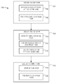
도 17은 일 예에 따른 처리 시스템에서 프로그램 가능 IC를 동작시키는 방법을 도시한 흐름도이다.
이해를 용이하게 하기 위해, 가능한 경우 도면에 공통인 동일한 요소를 지정하기 위해 동일한 참조 번호가 사용되었다. 하나의 예의 요소들이 다른 예들에 유리하게 통합될 수 있음이 고려된다.
Claims (15)
- 집적 회로(integrated circuit; IC) 패키지에 있어서,
기판 상에 배치된 처리 시스템 및 프로그램 가능 IC
를 포함하고, 상기 처리 시스템은 상기 기판의 인터커넥트를 통해 상기 프로그램 가능 IC에 결합되고,
상기 처리 시스템은 링 인터커넥트에 결합된 컴포넌트를 포함하며, 상기 컴포넌트는 프로세서 및 인터페이스 컨트롤러를 포함하고,
상기 프로그램 가능 IC는 상기 인터커넥트를 통해 상기 인터페이스 컨트롤러에 결합된 인터페이스 엔드 포인트; 및 상기 인터페이스 엔드 포인트에 결합되고 상기 인터페이스 엔드 포인트 및 상기 인터페이스 컨트롤러를 통해 상기 처리 시스템의 상기 링 인터커넥트와 통신하도록 구성된 적어도 하나의 주변 장치를 포함하는 것인, IC 패키지. - 제 1 항에 있어서, 상기 프로그램 가능 IC는 프로그램 가능 패브릭을 포함하는 것인, IC 패키지.
- 제 2 항에 있어서, 상기 프로그램 가능 IC는 상기 프로그램 가능 패브릭에 결합된 임베디드 처리 시스템을 포함하는 것인, IC 패키지.
- 제 2 항에 있어서, 상기 적어도 하나의 주변 장치는 상기 프로그램 가능 패브릭으로 프로그래밍되는 것인, IC 패키지.
- 제 1 항에 있어서, 상기 인터페이스 컨트롤러 및 상기 인터페이스 엔드 포인트는 각각 적어도 하나의 스트리밍 인터페이스를 사용하여 통신하도록 구성된 하나 이상의 포트를 포함하는 것인, IC 패키지.
- 제 1 항에 있어서, 상기 기판은 패키지 인터페이스를 포함하고, 상기 프로그램 가능 IC는 상기 패키지 인터페이스에 결합되는 것인, IC 패키지.
- 제 1 항에 있어서,
상기 처리 시스템 및 상기 프로그램 가능 IC에 결합된 하나 이상의 다른 IC
를 더 포함하는 IC 패키지. - 집적 회로(IC) 패키지에 있어서,
반도체 다이 상에 배치된 처리 시스템 및 프로그램 가능 IC
를 포함하고, 상기 처리 시스템은 링 인터커넥트에 결합된 컴포넌트를 포함하고, 상기 컴포넌트는 프로세서 및 인터페이스 회로를 포함하며;
상기 프로그램 가능 IC는 상기 링 인터커넥트에 결합되고 상기 링 인터커넥트와 통신하도록 구성된 적어도 하나의 주변 장치를 포함하는 것인, IC 패키지. - 제 8 항에 있어서, 상기 프로그램 가능 IC는 프로그램 가능 패브릭을 포함하는 것인, IC 패키지.
- 제 9 항에 있어서, 상기 프로그램 가능 IC는 상기 프로그램 가능 패브릭에 결합된 임베디드 처리 시스템을 포함하는 것인, IC 패키지.
- 제 9 항에 있어서, 상기 적어도 하나의 주변 장치는 상기 프로그램 가능 패브릭으로 프로그래밍되는 것인, IC 패키지.
- 제 8 항에 있어서, 상기 프로세서 및 상기 프로그램 가능 IC는 각각 적어도 하나의 스트리밍 인터페이스를 사용하여 통신하도록 구성된 하나 이상의 포트를 포함하는 것인, IC 패키지.
- 집적 회로(integrated circuit; IC) 패키지에 있어서,
반도체 다이 상에 배치된 처리 시스템 및 프로그램 가능 IC
를 포함하고, 상기 처리 시스템은 링 인터커넥트에 결합된 컴포넌트를 포함하고, 상기 컴포넌트는 프로세서, 인터페이스 회로 및 메모리를 포함하며;
상기 프로그램 가능 IC는 상기 링 인터커넥트에 결합되고 상기 링 인터커넥트와 통신하도록 구성된 적어도 하나의 주변 장치 및 적어도 하나의 메모리를 포함하는 것인, IC 패키지. - 제 13 항에 있어서, 상기 프로그램 가능 IC의 상기 적어도 하나의 메모리는 상기 링 인터커넥트에 결합되지 않는 것인, IC 패키지.
- 제 13 항에 있어서, 상기 프로그램 가능 IC의 상기 적어도 하나의 메모리는 상기 링 인터커넥트에 결합되는 것인, IC 패키지.
Applications Claiming Priority (3)
| Application Number | Priority Date | Filing Date | Title |
|---|---|---|---|
| US15/719,288 | 2017-09-28 | ||
| US15/719,288 US10573598B2 (en) | 2017-09-28 | 2017-09-28 | Integration of a programmable device and a processing system in an integrated circuit package |
| PCT/US2018/052413 WO2019067352A1 (en) | 2017-09-28 | 2018-09-24 | INTEGRATION OF A PROGRAMMABLE DEVICE AND A PROCESSING SYSTEM IN AN INTEGRATED CIRCUIT BOX |
Publications (2)
| Publication Number | Publication Date |
|---|---|
| KR20200062244A true KR20200062244A (ko) | 2020-06-03 |
| KR102759135B1 KR102759135B1 (ko) | 2025-01-22 |
Family
ID=63858108
Family Applications (1)
| Application Number | Title | Priority Date | Filing Date |
|---|---|---|---|
| KR1020207011292A Active KR102759135B1 (ko) | 2017-09-28 | 2018-09-24 | 집적 회로 패키지에 프로그램 가능 디바이스 및 처리 시스템의 통합 |
Country Status (6)
| Country | Link |
|---|---|
| US (2) | US10573598B2 (ko) |
| EP (2) | EP3688604B1 (ko) |
| JP (3) | JP7244497B2 (ko) |
| KR (1) | KR102759135B1 (ko) |
| CN (2) | CN111183419B (ko) |
| WO (1) | WO2019067352A1 (ko) |
Cited By (1)
| Publication number | Priority date | Publication date | Assignee | Title |
|---|---|---|---|---|
| KR20220091132A (ko) * | 2020-12-23 | 2022-06-30 | 주식회사 뉴티씨 (Newtc) | Avr 기반 아두이노 호환 보드를 위한 통합 프로그래머 및 기능 자동 설정 방법 |
Families Citing this family (13)
| Publication number | Priority date | Publication date | Assignee | Title |
|---|---|---|---|---|
| US11320995B2 (en) * | 2018-10-31 | 2022-05-03 | Western Digital Technologies, Inc. | Transferring computational operations to controllers of data storage devices |
| US10673439B1 (en) | 2019-03-27 | 2020-06-02 | Xilinx, Inc. | Adaptive integrated programmable device platform |
| US11474826B1 (en) * | 2019-04-18 | 2022-10-18 | Xilinx, Inc. | Boot image file having a global partition for data processing engines of a programmable device |
| US10990547B2 (en) * | 2019-08-11 | 2021-04-27 | Xilinx, Inc. | Dynamically reconfigurable networking using a programmable integrated circuit |
| US11580057B2 (en) | 2019-10-28 | 2023-02-14 | Xilinx, Inc. | Subsystem for configuration, security, and management of an adaptive system |
| US10720926B1 (en) | 2019-11-13 | 2020-07-21 | Xilinx, Inc. | Programmable device having hardened circuits for predetermined digital signal processing functionality |
| US11481317B2 (en) | 2020-06-26 | 2022-10-25 | Micron Technology, Inc. | Extended memory architecture |
| US11456951B1 (en) | 2021-04-08 | 2022-09-27 | Xilinx, Inc. | Flow table modification for network accelerators |
| US11606317B1 (en) | 2021-04-14 | 2023-03-14 | Xilinx, Inc. | Table based multi-function virtualization |
| US11971845B2 (en) * | 2022-06-16 | 2024-04-30 | Bae Systems Information And Electronic Systems Integration Inc. | DSP encapsulation |
| CN114880267B (zh) * | 2022-07-11 | 2022-10-04 | 南京芯驰半导体科技有限公司 | 一种多芯片互联系统及其方法 |
| US20240118671A1 (en) * | 2022-10-10 | 2024-04-11 | Schneider Electric Systems Usa, Inc. | Systems and methods for using memory-mapped memories in a microcontroller-based instrument |
| DE102024110515A1 (de) * | 2024-04-15 | 2025-10-16 | SECOR Supply Chain Transparency GmbH | Verfahren zum Anpassen eines integrierten Schaltkreises eines Vehikels |
Citations (3)
| Publication number | Priority date | Publication date | Assignee | Title |
|---|---|---|---|---|
| US7187709B1 (en) * | 2002-03-01 | 2007-03-06 | Xilinx, Inc. | High speed configurable transceiver architecture |
| KR20160096690A (ko) * | 2013-12-12 | 2016-08-16 | 마벨 월드 트레이드 리미티드 | 인트라-칩과 인터-칩 호핑 버스들을 통한 시스템-온-칩들 내의 그리고 시스템-온-칩들 간의 정보 전달을 위한 방법 및 장치 |
| US20170153892A1 (en) * | 2015-11-30 | 2017-06-01 | Intel Corporation | Instruction And Logic For Programmable Fabric Hierarchy And Cache |
Family Cites Families (27)
| Publication number | Priority date | Publication date | Assignee | Title |
|---|---|---|---|---|
| JPS6120349A (ja) * | 1984-07-06 | 1986-01-29 | Hitachi Ltd | Lsi集合体 |
| US5642058A (en) * | 1995-10-16 | 1997-06-24 | Xilinx , Inc. | Periphery input/output interconnect structure |
| JPH10209281A (ja) * | 1997-01-17 | 1998-08-07 | Fujitsu Ltd | フィールド・プログラマブル・ゲートアレイ |
| US6088421A (en) * | 1998-07-28 | 2000-07-11 | Intel Corporation | Method and apparatus for providing scaled ratio counters to obtain agent profiles |
| JP2002016489A (ja) | 2000-06-30 | 2002-01-18 | Fuji Xerox Co Ltd | プログラマブル論理回路装置、及び情報処理システム |
| US20030172189A1 (en) * | 2001-07-02 | 2003-09-11 | Globespanvirata Incorporated | Communications system using rings architecture |
| US6798239B2 (en) | 2001-09-28 | 2004-09-28 | Xilinx, Inc. | Programmable gate array having interconnecting logic to support embedded fixed logic circuitry |
| US7551564B2 (en) * | 2004-05-28 | 2009-06-23 | Intel Corporation | Flow control method and apparatus for single packet arrival on a bidirectional ring interconnect |
| JP4678717B2 (ja) * | 2004-12-27 | 2011-04-27 | ルネサスエレクトロニクス株式会社 | 半導体装置及び半導体装置の設計方法 |
| US7925802B2 (en) * | 2007-06-21 | 2011-04-12 | Seamicro Corp. | Hardware-based virtualization of BIOS, disks, network-interfaces, and consoles using a direct interconnect fabric |
| JP2011054041A (ja) | 2009-09-03 | 2011-03-17 | Fuji Xerox Co Ltd | 画像処理装置 |
| US8914672B2 (en) * | 2009-12-28 | 2014-12-16 | Intel Corporation | General purpose hardware to replace faulty core components that may also provide additional processor functionality |
| US9037688B2 (en) * | 2011-12-27 | 2015-05-19 | Intel Mobile Communications GmbH | System having trace resources |
| JP2015061164A (ja) * | 2013-09-18 | 2015-03-30 | 株式会社リコー | 電子機器、データ通信システム、および情報処理方法 |
| JP2015091045A (ja) * | 2013-11-06 | 2015-05-11 | シグナル・プロセス・ロジック株式会社 | プログラマブルロジックデバイスおよびこれを用いたコンピュータ |
| CN103678250B (zh) * | 2013-12-31 | 2017-04-05 | 赵建东 | 系统级芯片及其设计方法 |
| JP6504764B2 (ja) * | 2014-08-18 | 2019-04-24 | キヤノン株式会社 | 画像処理装置、画像処理装置の制御方法、及びプログラム |
| US10523585B2 (en) * | 2014-12-19 | 2019-12-31 | Amazon Technologies, Inc. | System on a chip comprising multiple compute sub-systems |
| WO2017005330A1 (en) * | 2015-07-09 | 2017-01-12 | Hitachi Data Systems Engineering UK Limited | Storage control system managing file-level and block-level storage services, and methods for controlling such storage control system |
| US9880966B1 (en) * | 2015-09-03 | 2018-01-30 | Xilinx, Inc. | Encapsulating metadata of a platform for application-specific tailoring and reuse of the platform in an integrated circuit |
| JP2017069777A (ja) * | 2015-09-30 | 2017-04-06 | 株式会社日立製作所 | 通信処理装置、通信方法および通信システム |
| US10229470B2 (en) * | 2016-08-05 | 2019-03-12 | Intel IP Corporation | Mechanism to accelerate graphics workloads in a multi-core computing architecture |
| US10540318B2 (en) * | 2017-04-09 | 2020-01-21 | Intel Corporation | Graphics processing integrated circuit package |
| US10102149B1 (en) * | 2017-04-17 | 2018-10-16 | Intel Corporation | Replacement policies for a hybrid hierarchical cache |
| US11080810B2 (en) * | 2017-04-21 | 2021-08-03 | Intel Corporation | Dynamically reconfigurable memory subsystem for graphics processors |
| US20180329855A1 (en) * | 2017-05-12 | 2018-11-15 | Intel Corporation | Alternate protocol negotiation in a high performance interconnect |
| US11394649B2 (en) * | 2018-06-29 | 2022-07-19 | Intel Corporation | Non-random flowlet-based routing |
-
2017
- 2017-09-28 US US15/719,288 patent/US10573598B2/en active Active
-
2018
- 2018-09-24 KR KR1020207011292A patent/KR102759135B1/ko active Active
- 2018-09-24 WO PCT/US2018/052413 patent/WO2019067352A1/en not_active Ceased
- 2018-09-24 JP JP2020517780A patent/JP7244497B2/ja active Active
- 2018-09-24 CN CN201880063416.4A patent/CN111183419B/zh active Active
- 2018-09-24 CN CN202410368756.5A patent/CN118295958A/zh active Pending
- 2018-09-24 EP EP18786532.4A patent/EP3688604B1/en active Active
- 2018-09-24 EP EP23191968.9A patent/EP4254214A3/en active Pending
-
2020
- 2020-01-27 US US16/773,501 patent/US11024583B2/en active Active
-
2023
- 2023-03-09 JP JP2023036854A patent/JP7599514B2/ja active Active
-
2024
- 2024-08-14 JP JP2024135331A patent/JP2024161478A/ja not_active Withdrawn
Patent Citations (3)
| Publication number | Priority date | Publication date | Assignee | Title |
|---|---|---|---|---|
| US7187709B1 (en) * | 2002-03-01 | 2007-03-06 | Xilinx, Inc. | High speed configurable transceiver architecture |
| KR20160096690A (ko) * | 2013-12-12 | 2016-08-16 | 마벨 월드 트레이드 리미티드 | 인트라-칩과 인터-칩 호핑 버스들을 통한 시스템-온-칩들 내의 그리고 시스템-온-칩들 간의 정보 전달을 위한 방법 및 장치 |
| US20170153892A1 (en) * | 2015-11-30 | 2017-06-01 | Intel Corporation | Instruction And Logic For Programmable Fabric Hierarchy And Cache |
Cited By (1)
| Publication number | Priority date | Publication date | Assignee | Title |
|---|---|---|---|---|
| KR20220091132A (ko) * | 2020-12-23 | 2022-06-30 | 주식회사 뉴티씨 (Newtc) | Avr 기반 아두이노 호환 보드를 위한 통합 프로그래머 및 기능 자동 설정 방법 |
Also Published As
| Publication number | Publication date |
|---|---|
| EP3688604B1 (en) | 2023-08-23 |
| EP3688604A1 (en) | 2020-08-05 |
| EP4254214A3 (en) | 2023-12-13 |
| JP7244497B2 (ja) | 2023-03-22 |
| CN111183419B (zh) | 2024-04-16 |
| JP2020535659A (ja) | 2020-12-03 |
| CN118295958A (zh) | 2024-07-05 |
| JP7599514B2 (ja) | 2024-12-13 |
| JP2024161478A (ja) | 2024-11-19 |
| US10573598B2 (en) | 2020-02-25 |
| JP2023078246A (ja) | 2023-06-06 |
| US20190096813A1 (en) | 2019-03-28 |
| US11024583B2 (en) | 2021-06-01 |
| EP4254214A2 (en) | 2023-10-04 |
| US20200161247A1 (en) | 2020-05-21 |
| WO2019067352A1 (en) | 2019-04-04 |
| CN111183419A (zh) | 2020-05-19 |
| KR102759135B1 (ko) | 2025-01-22 |
Similar Documents
| Publication | Publication Date | Title |
|---|---|---|
| JP7599514B2 (ja) | 集積回路パッケージへのプログラマブルデバイスおよび処理システムの集積 | |
| KR102827630B1 (ko) | 프로그래머블 디바이스를 위한 구성 가능한 네트워크-온-칩 | |
| US11182110B1 (en) | On-chip memory block circuit | |
| CN108139916B (zh) | 可编程逻辑设备的多阶段引导映像加载和配置 | |
| JP2018531461A6 (ja) | マルチステージブートイメージロードおよびプログラマブルロジックデバイスの構成 | |
| US20170097910A1 (en) | Direct memory access for programmable logic device configuration | |
| US10936486B1 (en) | Address interleave support in a programmable device | |
| JP7402798B2 (ja) | データセンタにおけるプログラマブルデバイス向けのセキュリティ | |
| KR102851915B1 (ko) | 프로그래밍가능 디바이스 구성 메모리 시스템 | |
| US11327899B1 (en) | Hardware-based virtual-to-physical address translation for programmable logic masters in a system on chip | |
| US11474555B1 (en) | Data-driven platform characteristics capture and discovery for hardware accelerators | |
| US11874768B1 (en) | Flash memory emulation |
Legal Events
| Date | Code | Title | Description |
|---|---|---|---|
| E13-X000 | Pre-grant limitation requested |
St.27 status event code: A-2-3-E10-E13-lim-X000 |
|
| PA0105 | International application |
St.27 status event code: A-0-1-A10-A15-nap-PA0105 |
|
| P11-X000 | Amendment of application requested |
St.27 status event code: A-2-2-P10-P11-nap-X000 |
|
| P13-X000 | Application amended |
St.27 status event code: A-2-2-P10-P13-nap-X000 |
|
| PG1501 | Laying open of application |
St.27 status event code: A-1-1-Q10-Q12-nap-PG1501 |
|
| A201 | Request for examination | ||
| PA0201 | Request for examination |
St.27 status event code: A-1-2-D10-D11-exm-PA0201 |
|
| D13-X000 | Search requested |
St.27 status event code: A-1-2-D10-D13-srh-X000 |
|
| D14-X000 | Search report completed |
St.27 status event code: A-1-2-D10-D14-srh-X000 |
|
| E902 | Notification of reason for refusal | ||
| PE0902 | Notice of grounds for rejection |
St.27 status event code: A-1-2-D10-D21-exm-PE0902 |
|
| P11-X000 | Amendment of application requested |
St.27 status event code: A-2-2-P10-P11-nap-X000 |
|
| P13-X000 | Application amended |
St.27 status event code: A-2-2-P10-P13-nap-X000 |
|
| E701 | Decision to grant or registration of patent right | ||
| PE0701 | Decision of registration |
St.27 status event code: A-1-2-D10-D22-exm-PE0701 |
|
| GRNT | Written decision to grant | ||
| PR0701 | Registration of establishment |
St.27 status event code: A-2-4-F10-F11-exm-PR0701 |
|
| PR1002 | Payment of registration fee |
St.27 status event code: A-2-2-U10-U12-oth-PR1002 Fee payment year number: 1 |
|
| PG1601 | Publication of registration |
St.27 status event code: A-4-4-Q10-Q13-nap-PG1601 |
|
| P22-X000 | Classification modified |
St.27 status event code: A-4-4-P10-P22-nap-X000 |