KR20200062360A - 공간 분리를 갖는 단일 웨이퍼 프로세싱 환경들 - Google Patents
공간 분리를 갖는 단일 웨이퍼 프로세싱 환경들 Download PDFInfo
- Publication number
- KR20200062360A KR20200062360A KR1020207014767A KR20207014767A KR20200062360A KR 20200062360 A KR20200062360 A KR 20200062360A KR 1020207014767 A KR1020207014767 A KR 1020207014767A KR 20207014767 A KR20207014767 A KR 20207014767A KR 20200062360 A KR20200062360 A KR 20200062360A
- Authority
- KR
- South Korea
- Prior art keywords
- support
- heater
- heaters
- support assembly
- processing
- Prior art date
- Legal status (The legal status is an assumption and is not a legal conclusion. Google has not performed a legal analysis and makes no representation as to the accuracy of the status listed.)
- Granted
Links
Images


Classifications
-
- H—ELECTRICITY
- H10—SEMICONDUCTOR DEVICES; ELECTRIC SOLID-STATE DEVICES NOT OTHERWISE PROVIDED FOR
- H10P—GENERIC PROCESSES OR APPARATUS FOR THE MANUFACTURE OR TREATMENT OF DEVICES COVERED BY CLASS H10
- H10P72/00—Handling or holding of wafers, substrates or devices during manufacture or treatment thereof
- H10P72/70—Handling or holding of wafers, substrates or devices during manufacture or treatment thereof for supporting or gripping
- H10P72/76—Handling or holding of wafers, substrates or devices during manufacture or treatment thereof for supporting or gripping using mechanical means, e.g. clamps or pinches
- H10P72/7604—Handling or holding of wafers, substrates or devices during manufacture or treatment thereof for supporting or gripping using mechanical means, e.g. clamps or pinches the wafers being placed on a susceptor, stage or support
- H10P72/7624—Handling or holding of wafers, substrates or devices during manufacture or treatment thereof for supporting or gripping using mechanical means, e.g. clamps or pinches the wafers being placed on a susceptor, stage or support characterised by the mechanical construction of the susceptor, stage or support
-
- C—CHEMISTRY; METALLURGY
- C23—COATING METALLIC MATERIAL; COATING MATERIAL WITH METALLIC MATERIAL; CHEMICAL SURFACE TREATMENT; DIFFUSION TREATMENT OF METALLIC MATERIAL; COATING BY VACUUM EVAPORATION, BY SPUTTERING, BY ION IMPLANTATION OR BY CHEMICAL VAPOUR DEPOSITION, IN GENERAL; INHIBITING CORROSION OF METALLIC MATERIAL OR INCRUSTATION IN GENERAL
- C23C—COATING METALLIC MATERIAL; COATING MATERIAL WITH METALLIC MATERIAL; SURFACE TREATMENT OF METALLIC MATERIAL BY DIFFUSION INTO THE SURFACE, BY CHEMICAL CONVERSION OR SUBSTITUTION; COATING BY VACUUM EVAPORATION, BY SPUTTERING, BY ION IMPLANTATION OR BY CHEMICAL VAPOUR DEPOSITION, IN GENERAL
- C23C16/00—Chemical coating by decomposition of gaseous compounds, without leaving reaction products of surface material in the coating, i.e. chemical vapour deposition [CVD] processes
- C23C16/44—Chemical coating by decomposition of gaseous compounds, without leaving reaction products of surface material in the coating, i.e. chemical vapour deposition [CVD] processes characterised by the method of coating
- C23C16/458—Chemical coating by decomposition of gaseous compounds, without leaving reaction products of surface material in the coating, i.e. chemical vapour deposition [CVD] processes characterised by the method of coating characterised by the method used for supporting substrates in the reaction chamber
- C23C16/4582—Rigid and flat substrates, e.g. plates or discs
- C23C16/4583—Rigid and flat substrates, e.g. plates or discs the substrate being supported substantially horizontally
- C23C16/4584—Rigid and flat substrates, e.g. plates or discs the substrate being supported substantially horizontally the substrate being rotated
-
- C—CHEMISTRY; METALLURGY
- C23—COATING METALLIC MATERIAL; COATING MATERIAL WITH METALLIC MATERIAL; CHEMICAL SURFACE TREATMENT; DIFFUSION TREATMENT OF METALLIC MATERIAL; COATING BY VACUUM EVAPORATION, BY SPUTTERING, BY ION IMPLANTATION OR BY CHEMICAL VAPOUR DEPOSITION, IN GENERAL; INHIBITING CORROSION OF METALLIC MATERIAL OR INCRUSTATION IN GENERAL
- C23C—COATING METALLIC MATERIAL; COATING MATERIAL WITH METALLIC MATERIAL; SURFACE TREATMENT OF METALLIC MATERIAL BY DIFFUSION INTO THE SURFACE, BY CHEMICAL CONVERSION OR SUBSTITUTION; COATING BY VACUUM EVAPORATION, BY SPUTTERING, BY ION IMPLANTATION OR BY CHEMICAL VAPOUR DEPOSITION, IN GENERAL
- C23C16/00—Chemical coating by decomposition of gaseous compounds, without leaving reaction products of surface material in the coating, i.e. chemical vapour deposition [CVD] processes
- C23C16/44—Chemical coating by decomposition of gaseous compounds, without leaving reaction products of surface material in the coating, i.e. chemical vapour deposition [CVD] processes characterised by the method of coating
- C23C16/4401—Means for minimising impurities, e.g. dust, moisture or residual gas, in the reaction chamber
- C23C16/4409—Means for minimising impurities, e.g. dust, moisture or residual gas, in the reaction chamber characterised by sealing means
-
- C—CHEMISTRY; METALLURGY
- C23—COATING METALLIC MATERIAL; COATING MATERIAL WITH METALLIC MATERIAL; CHEMICAL SURFACE TREATMENT; DIFFUSION TREATMENT OF METALLIC MATERIAL; COATING BY VACUUM EVAPORATION, BY SPUTTERING, BY ION IMPLANTATION OR BY CHEMICAL VAPOUR DEPOSITION, IN GENERAL; INHIBITING CORROSION OF METALLIC MATERIAL OR INCRUSTATION IN GENERAL
- C23C—COATING METALLIC MATERIAL; COATING MATERIAL WITH METALLIC MATERIAL; SURFACE TREATMENT OF METALLIC MATERIAL BY DIFFUSION INTO THE SURFACE, BY CHEMICAL CONVERSION OR SUBSTITUTION; COATING BY VACUUM EVAPORATION, BY SPUTTERING, BY ION IMPLANTATION OR BY CHEMICAL VAPOUR DEPOSITION, IN GENERAL
- C23C16/00—Chemical coating by decomposition of gaseous compounds, without leaving reaction products of surface material in the coating, i.e. chemical vapour deposition [CVD] processes
- C23C16/44—Chemical coating by decomposition of gaseous compounds, without leaving reaction products of surface material in the coating, i.e. chemical vapour deposition [CVD] processes characterised by the method of coating
- C23C16/455—Chemical coating by decomposition of gaseous compounds, without leaving reaction products of surface material in the coating, i.e. chemical vapour deposition [CVD] processes characterised by the method of coating characterised by the method used for introducing gases into reaction chamber or for modifying gas flows in reaction chamber
- C23C16/45523—Pulsed gas flow or change of composition over time
- C23C16/45525—Atomic layer deposition [ALD]
- C23C16/45544—Atomic layer deposition [ALD] characterized by the apparatus
- C23C16/45548—Atomic layer deposition [ALD] characterized by the apparatus having arrangements for gas injection at different locations of the reactor for each ALD half-reaction
- C23C16/45551—Atomic layer deposition [ALD] characterized by the apparatus having arrangements for gas injection at different locations of the reactor for each ALD half-reaction for relative movement of the substrate and the gas injectors or half-reaction reactor compartments
-
- C—CHEMISTRY; METALLURGY
- C23—COATING METALLIC MATERIAL; COATING MATERIAL WITH METALLIC MATERIAL; CHEMICAL SURFACE TREATMENT; DIFFUSION TREATMENT OF METALLIC MATERIAL; COATING BY VACUUM EVAPORATION, BY SPUTTERING, BY ION IMPLANTATION OR BY CHEMICAL VAPOUR DEPOSITION, IN GENERAL; INHIBITING CORROSION OF METALLIC MATERIAL OR INCRUSTATION IN GENERAL
- C23C—COATING METALLIC MATERIAL; COATING MATERIAL WITH METALLIC MATERIAL; SURFACE TREATMENT OF METALLIC MATERIAL BY DIFFUSION INTO THE SURFACE, BY CHEMICAL CONVERSION OR SUBSTITUTION; COATING BY VACUUM EVAPORATION, BY SPUTTERING, BY ION IMPLANTATION OR BY CHEMICAL VAPOUR DEPOSITION, IN GENERAL
- C23C16/00—Chemical coating by decomposition of gaseous compounds, without leaving reaction products of surface material in the coating, i.e. chemical vapour deposition [CVD] processes
- C23C16/44—Chemical coating by decomposition of gaseous compounds, without leaving reaction products of surface material in the coating, i.e. chemical vapour deposition [CVD] processes characterised by the method of coating
- C23C16/455—Chemical coating by decomposition of gaseous compounds, without leaving reaction products of surface material in the coating, i.e. chemical vapour deposition [CVD] processes characterised by the method of coating characterised by the method used for introducing gases into reaction chamber or for modifying gas flows in reaction chamber
- C23C16/45563—Gas nozzles
- C23C16/45565—Shower nozzles
-
- C—CHEMISTRY; METALLURGY
- C23—COATING METALLIC MATERIAL; COATING MATERIAL WITH METALLIC MATERIAL; CHEMICAL SURFACE TREATMENT; DIFFUSION TREATMENT OF METALLIC MATERIAL; COATING BY VACUUM EVAPORATION, BY SPUTTERING, BY ION IMPLANTATION OR BY CHEMICAL VAPOUR DEPOSITION, IN GENERAL; INHIBITING CORROSION OF METALLIC MATERIAL OR INCRUSTATION IN GENERAL
- C23C—COATING METALLIC MATERIAL; COATING MATERIAL WITH METALLIC MATERIAL; SURFACE TREATMENT OF METALLIC MATERIAL BY DIFFUSION INTO THE SURFACE, BY CHEMICAL CONVERSION OR SUBSTITUTION; COATING BY VACUUM EVAPORATION, BY SPUTTERING, BY ION IMPLANTATION OR BY CHEMICAL VAPOUR DEPOSITION, IN GENERAL
- C23C16/00—Chemical coating by decomposition of gaseous compounds, without leaving reaction products of surface material in the coating, i.e. chemical vapour deposition [CVD] processes
- C23C16/44—Chemical coating by decomposition of gaseous compounds, without leaving reaction products of surface material in the coating, i.e. chemical vapour deposition [CVD] processes characterised by the method of coating
- C23C16/458—Chemical coating by decomposition of gaseous compounds, without leaving reaction products of surface material in the coating, i.e. chemical vapour deposition [CVD] processes characterised by the method of coating characterised by the method used for supporting substrates in the reaction chamber
- C23C16/4582—Rigid and flat substrates, e.g. plates or discs
- C23C16/4583—Rigid and flat substrates, e.g. plates or discs the substrate being supported substantially horizontally
- C23C16/4586—Elements in the interior of the support, e.g. electrodes, heating or cooling devices
-
- C—CHEMISTRY; METALLURGY
- C23—COATING METALLIC MATERIAL; COATING MATERIAL WITH METALLIC MATERIAL; CHEMICAL SURFACE TREATMENT; DIFFUSION TREATMENT OF METALLIC MATERIAL; COATING BY VACUUM EVAPORATION, BY SPUTTERING, BY ION IMPLANTATION OR BY CHEMICAL VAPOUR DEPOSITION, IN GENERAL; INHIBITING CORROSION OF METALLIC MATERIAL OR INCRUSTATION IN GENERAL
- C23C—COATING METALLIC MATERIAL; COATING MATERIAL WITH METALLIC MATERIAL; SURFACE TREATMENT OF METALLIC MATERIAL BY DIFFUSION INTO THE SURFACE, BY CHEMICAL CONVERSION OR SUBSTITUTION; COATING BY VACUUM EVAPORATION, BY SPUTTERING, BY ION IMPLANTATION OR BY CHEMICAL VAPOUR DEPOSITION, IN GENERAL
- C23C16/00—Chemical coating by decomposition of gaseous compounds, without leaving reaction products of surface material in the coating, i.e. chemical vapour deposition [CVD] processes
- C23C16/44—Chemical coating by decomposition of gaseous compounds, without leaving reaction products of surface material in the coating, i.e. chemical vapour deposition [CVD] processes characterised by the method of coating
- C23C16/46—Chemical coating by decomposition of gaseous compounds, without leaving reaction products of surface material in the coating, i.e. chemical vapour deposition [CVD] processes characterised by the method of coating characterised by the method used for heating the substrate
-
- H01L21/0228—
-
- H01L21/67103—
-
- H01L21/683—
-
- H—ELECTRICITY
- H10—SEMICONDUCTOR DEVICES; ELECTRIC SOLID-STATE DEVICES NOT OTHERWISE PROVIDED FOR
- H10P—GENERIC PROCESSES OR APPARATUS FOR THE MANUFACTURE OR TREATMENT OF DEVICES COVERED BY CLASS H10
- H10P72/00—Handling or holding of wafers, substrates or devices during manufacture or treatment thereof
- H10P72/04—Apparatus for manufacture or treatment
- H10P72/0431—Apparatus for thermal treatment
- H10P72/0432—Apparatus for thermal treatment mainly by conduction
-
- H—ELECTRICITY
- H10—SEMICONDUCTOR DEVICES; ELECTRIC SOLID-STATE DEVICES NOT OTHERWISE PROVIDED FOR
- H10P—GENERIC PROCESSES OR APPARATUS FOR THE MANUFACTURE OR TREATMENT OF DEVICES COVERED BY CLASS H10
- H10P72/00—Handling or holding of wafers, substrates or devices during manufacture or treatment thereof
- H10P72/04—Apparatus for manufacture or treatment
- H10P72/0451—Apparatus for manufacturing or treating in a plurality of work-stations
- H10P72/0462—Apparatus for manufacturing or treating in a plurality of work-stations characterised by the construction of the processing chambers, e.g. modular processing chambers
-
- H—ELECTRICITY
- H10—SEMICONDUCTOR DEVICES; ELECTRIC SOLID-STATE DEVICES NOT OTHERWISE PROVIDED FOR
- H10P—GENERIC PROCESSES OR APPARATUS FOR THE MANUFACTURE OR TREATMENT OF DEVICES COVERED BY CLASS H10
- H10P72/00—Handling or holding of wafers, substrates or devices during manufacture or treatment thereof
- H10P72/06—Apparatus for monitoring, sorting, marking, testing or measuring
- H10P72/0602—Temperature monitoring
-
- H—ELECTRICITY
- H10—SEMICONDUCTOR DEVICES; ELECTRIC SOLID-STATE DEVICES NOT OTHERWISE PROVIDED FOR
- H10P—GENERIC PROCESSES OR APPARATUS FOR THE MANUFACTURE OR TREATMENT OF DEVICES COVERED BY CLASS H10
- H10P72/00—Handling or holding of wafers, substrates or devices during manufacture or treatment thereof
- H10P72/70—Handling or holding of wafers, substrates or devices during manufacture or treatment thereof for supporting or gripping
- H10P72/72—Handling or holding of wafers, substrates or devices during manufacture or treatment thereof for supporting or gripping using electrostatic chucks
- H10P72/722—Details of electrostatic chucks
-
- H—ELECTRICITY
- H10—SEMICONDUCTOR DEVICES; ELECTRIC SOLID-STATE DEVICES NOT OTHERWISE PROVIDED FOR
- H10P—GENERIC PROCESSES OR APPARATUS FOR THE MANUFACTURE OR TREATMENT OF DEVICES COVERED BY CLASS H10
- H10P72/00—Handling or holding of wafers, substrates or devices during manufacture or treatment thereof
- H10P72/70—Handling or holding of wafers, substrates or devices during manufacture or treatment thereof for supporting or gripping
- H10P72/76—Handling or holding of wafers, substrates or devices during manufacture or treatment thereof for supporting or gripping using mechanical means, e.g. clamps or pinches
- H10P72/7604—Handling or holding of wafers, substrates or devices during manufacture or treatment thereof for supporting or gripping using mechanical means, e.g. clamps or pinches the wafers being placed on a susceptor, stage or support
- H10P72/7618—Handling or holding of wafers, substrates or devices during manufacture or treatment thereof for supporting or gripping using mechanical means, e.g. clamps or pinches the wafers being placed on a susceptor, stage or support characterised by a movable susceptor, stage or support, others than those only rotating on their own vertical axis, e.g. susceptors on a rotating carrousel
-
- H—ELECTRICITY
- H10—SEMICONDUCTOR DEVICES; ELECTRIC SOLID-STATE DEVICES NOT OTHERWISE PROVIDED FOR
- H10P—GENERIC PROCESSES OR APPARATUS FOR THE MANUFACTURE OR TREATMENT OF DEVICES COVERED BY CLASS H10
- H10P72/00—Handling or holding of wafers, substrates or devices during manufacture or treatment thereof
- H10P72/70—Handling or holding of wafers, substrates or devices during manufacture or treatment thereof for supporting or gripping
- H10P72/76—Handling or holding of wafers, substrates or devices during manufacture or treatment thereof for supporting or gripping using mechanical means, e.g. clamps or pinches
- H10P72/7604—Handling or holding of wafers, substrates or devices during manufacture or treatment thereof for supporting or gripping using mechanical means, e.g. clamps or pinches the wafers being placed on a susceptor, stage or support
- H10P72/7621—Handling or holding of wafers, substrates or devices during manufacture or treatment thereof for supporting or gripping using mechanical means, e.g. clamps or pinches the wafers being placed on a susceptor, stage or support characterised by supporting two or more semiconductor substrates
Landscapes
- Chemical & Material Sciences (AREA)
- General Chemical & Material Sciences (AREA)
- Chemical Kinetics & Catalysis (AREA)
- Engineering & Computer Science (AREA)
- Materials Engineering (AREA)
- Mechanical Engineering (AREA)
- Metallurgy (AREA)
- Organic Chemistry (AREA)
- Container, Conveyance, Adherence, Positioning, Of Wafer (AREA)
- Chemical Vapour Deposition (AREA)
- Analysing Materials By The Use Of Radiation (AREA)
- Mechanical Treatment Of Semiconductor (AREA)
- Plasma Technology (AREA)
Abstract
Description
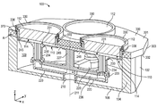
[0010] 도 1은 본 개시내용의 하나 이상의 실시예에 따른 프로세싱 챔버의 등각 단면도를 도시한다.
[0011] 도 2는 본 개시내용의 하나 이상의 실시예에 따른 프로세싱 챔버의 단면도를 도시한다.
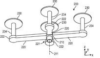
[0012] 도 3은 본 개시내용의 하나 이상의 실시예에 따른 지지 조립체의 평행 투영 저면도를 도시한다.
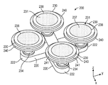
[0013] 도 4는 본 개시내용의 하나 이상의 실시예에 따른 지지 조립체의 평행 투영 평면도를 도시한다.
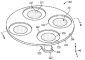
[0014] 도 5는 본 개시내용의 하나 이상의 실시예에 따른 지지 조립체의 평행 투영 평면도를 도시한다.
[0015] 도 6은 본 개시내용의 하나 이상의 실시예에 따른 지지 조립체의 측단면도를 도시한다.
[0016] 도 7은 본 개시내용의 하나 이상의 실시예에 따른 지지 조립체의 부분 측단면도를 도시한다.
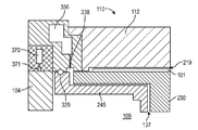
[0017] 도 8은 본 개시내용의 하나 이상의 실시예에 따른 지지 조립체의 부분 측단면도를 도시한다.
[0018] 도 9는 본 개시내용의 하나 이상의 실시예에 따른 지지 조립체의 부분 측단면도이다.
[0019] 도 10a는 본 개시내용의 하나 이상의 실시예에 따른 지지 플레이트의 등각 평면도이다.
[0020] 도 10b는 라인 10B-10B'를 따라 취해진 도 10a의 지지 플레이트의 측단면도이다.
[0021] 도 11a는 본 개시내용의 하나 이상의 실시예에 따른 지지 플레이트의 등각 저면도이다.
[0022] 도 11b는 라인 11B-11B'를 따라 취해진 도 11a의 지지 플레이트의 측단면도이다.
[0023] 도 12a는 본 개시내용의 하나 이상의 실시예에 따른 지지 플레이트의 등각 저면도이다.
[0024] 도 12b는 라인 12B-12B'를 따라 취해진 도 12a의 지지 플레이트의 측단면도이다.
[0025] 도 13은 본 개시내용의 하나 이상의 실시예에 따른, 프로세싱 챔버를 위한 최상부 플레이트의 등각 단면도이다.
[0026] 도 14는 본 개시내용의 하나 이상의 실시예에 따른 프로세스 스테이션의 분해 단면도이다.
[0027] 도 15는 본 개시내용의 하나 이상의 실시예에 따른, 프로세싱 챔버를 위한 최상부 플레이트의 개략적인 측단면도이다.
[0028] 도 16은 본 개시내용의 하나 이상의 실시예에 따른, 프로세싱 챔버 내의 프로세스 스테이션의 부분 측단면도이다.
[0029] 도 17은 본 개시내용의 하나 이상의 실시예에 따른 프로세싱 플랫폼의 개략적인 표현이다.
[0030] 도 18a 내지 도 18i는 본 개시내용의 하나 이상의 실시예에 따른, 프로세싱 챔버 내의 프로세스 스테이션 구성들의 개략도들을 도시한다.
[0031] 도 19a 및 도 19b는 본 개시내용의 하나 이상의 실시예에 따른 프로세스의 개략적인 표현들을 도시한다.
[0032] 도 20은 본 개시내용의 하나 이상의 실시예에 따른 지지 조립체의 개략적인 단면 표현을 도시한다.
Claims (15)
- 회전 축을 정의하는 회전가능 중앙 베이스;
상기 중앙 베이스로부터 연장되는 적어도 2개의 지지 암들 ― 상기 지지 암들 각각은 상기 중앙 베이스와 접촉하는 내측 단부, 및 외측 단부를 가짐 ―; 및
상기 지지 암들 각각의 외측 단부 상에 포지셔닝된 가열기
를 포함하며,
가열기들은 지지 표면을 갖는,
지지 조립체. - 제1 항에 있어서,
상기 지지 암들은 상기 회전 축에 직각으로 연장되는,
지지 조립체. - 제1 항에 있어서,
3개의 지지 암들 및 3개의 가열기들이 있는,
지지 조립체. - 제1 항에 있어서,
4개의 지지 암들 및 4개의 가열기들이 있는,
지지 조립체. - 제1 항에 있어서,
상기 가열기의 지지 표면들은 실질적으로 동일 평면에 있는,
지지 조립체. - 제1 항에 있어서,
상기 가열기들의 중심은, 상기 중앙 베이스의 회전 시에 상기 가열기들이 원형 경로로 이동하도록, 상기 회전 축으로부터 일정 거리에 위치되는,
지지 조립체. - 제1 항에 있어서,
상기 중앙 베이스에 연결된 적어도 하나의 모터를 더 포함하며,
상기 적어도 하나의 모터는 상기 회전 축을 중심으로 상기 지지 조립체를 회전시키도록 구성되는,
지지 조립체. - 제1 항에 있어서,
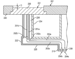
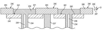
상기 가열기들 주위에 포지셔닝된 적어도 하나의 밀봉 플랫폼을 더 포함하며,
상기 밀봉 플랫폼은 상기 가열기의 지지 표면에 의해 형성되는 주 평면과 실질적으로 평행한 주 평면을 형성하는 최상부 표면을 갖는,
지지 조립체. - 제8 항에 있어서,
각각의 가열기는 상기 가열기 주위에 포지셔닝된 밀봉 플랫폼을 갖고, 밀봉 플랫폼들은 링 형상 최상부 표면을 형성하는,
지지 조립체. - 제8 항에 있어서,
하나의 밀봉 플랫폼이 있으며, 상기 하나의 밀봉 플랫폼은 상기 가열기들 각각이 상기 밀봉 플랫폼을 통과하기 위한 개구들을 갖는,
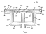
지지 조립체. - 내부 볼륨을 정의하는, 벽들, 최하부, 및 최상부를 갖는 하우징(housing);
상기 하우징의 내부 볼륨 내의 복수의 프로세스 스테이션들 ― 상기 프로세스 스테이션들은 회전 축 주위에 원형 어레인지먼트(arrangement)로 포지셔닝되고, 각각의 프로세스 스테이션은 전방 면을 갖는 가스 주입기를 포함하고, 가스 주입기들 각각의 전방 면은 실질적으로 동일 평면에 있음 ―; 및
상기 하우징의 내부 볼륨 내의 지지 조립체
를 포함하며,
상기 지지 조립체는 상기 복수의 프로세스 스테이션들 아래에 포지셔닝되고, 상기 지지 조립체는 복수의 지지 암들을 갖는 회전가능 중앙 베이스를 포함하고, 상기 복수의 지지 암들은 상기 중앙 베이스로부터 연장되고, 각각의 지지 암은 상기 중앙 베이스와 접촉하는 내측 단부, 및 외측 단부를 갖고, 상기 지지 암들 각각의 외측 단부 상에 가열기가 포지셔닝되고, 가열기들은 지지 표면을 갖는,
프로세싱 챔버. - 제11 항에 있어서,
상기 가열기들의 지지 표면들 각각이 동시에 상이한 프로세스 스테이션의 전방 면에 인접하게 위치될 수 있도록 구성된 동일한 수의 가열기들, 지지 암들, 및 프로세스 스테이션들이 있는,
프로세싱 챔버. - 제11 항에 있어서,
상기 가열기의 지지 표면들은 실질적으로 동일 평면에 있는,
프로세싱 챔버. - 제11 항에 있어서,
상기 중앙 베이스에 연결된 적어도 하나의 모터를 더 포함하며,
상기 적어도 하나의 모터는 상기 회전 축을 중심으로 상기 지지 조립체를 회전시키도록 구성되는,
프로세싱 챔버. - 제11 항에 있어서,
각각의 가열기는 상기 가열기 주위에 포지셔닝된 밀봉 플랫폼을 더 포함하며, 상기 밀봉 플랫폼은 상기 가열기의 지지 표면에 의해 형성되는 주 평면과 실질적으로 평행한 주 평면을 형성하는 최상부 표면을 갖는,
프로세싱 챔버.
Priority Applications (1)
| Application Number | Priority Date | Filing Date | Title |
|---|---|---|---|
| KR1020227010807A KR102614522B1 (ko) | 2017-10-27 | 2018-10-26 | 공간 분리를 갖는 단일 웨이퍼 프로세싱 환경들 |
Applications Claiming Priority (3)
| Application Number | Priority Date | Filing Date | Title |
|---|---|---|---|
| US201762578365P | 2017-10-27 | 2017-10-27 | |
| US62/578,365 | 2017-10-27 | ||
| PCT/US2018/057685 WO2019084386A1 (en) | 2017-10-27 | 2018-10-26 | SINGLE WAFER PROCESSING ENVIRONMENTS WITH SPACE SEPARATION |
Related Child Applications (1)
| Application Number | Title | Priority Date | Filing Date |
|---|---|---|---|
| KR1020227010807A Division KR102614522B1 (ko) | 2017-10-27 | 2018-10-26 | 공간 분리를 갖는 단일 웨이퍼 프로세싱 환경들 |
Publications (2)
| Publication Number | Publication Date |
|---|---|
| KR20200062360A true KR20200062360A (ko) | 2020-06-03 |
| KR102383687B1 KR102383687B1 (ko) | 2022-04-08 |
Family
ID=66244211
Family Applications (5)
| Application Number | Title | Priority Date | Filing Date |
|---|---|---|---|
| KR1020207014767A Active KR102383687B1 (ko) | 2017-10-27 | 2018-10-26 | 공간 분리를 갖는 단일 웨이퍼 프로세싱 환경들 |
| KR1020237021324A Active KR102735771B1 (ko) | 2017-10-27 | 2018-10-26 | 공간 분리를 갖는 단일 웨이퍼 프로세싱 환경들 |
| KR1020247039204A Active KR102814629B1 (ko) | 2017-10-27 | 2018-10-26 | 공간 분리를 갖는 단일 웨이퍼 프로세싱 환경들 |
| KR1020257017274A Pending KR20250080916A (ko) | 2017-10-27 | 2018-10-26 | 공간 분리를 갖는 단일 웨이퍼 프로세싱 환경들 |
| KR1020227010807A Active KR102614522B1 (ko) | 2017-10-27 | 2018-10-26 | 공간 분리를 갖는 단일 웨이퍼 프로세싱 환경들 |
Family Applications After (4)
| Application Number | Title | Priority Date | Filing Date |
|---|---|---|---|
| KR1020237021324A Active KR102735771B1 (ko) | 2017-10-27 | 2018-10-26 | 공간 분리를 갖는 단일 웨이퍼 프로세싱 환경들 |
| KR1020247039204A Active KR102814629B1 (ko) | 2017-10-27 | 2018-10-26 | 공간 분리를 갖는 단일 웨이퍼 프로세싱 환경들 |
| KR1020257017274A Pending KR20250080916A (ko) | 2017-10-27 | 2018-10-26 | 공간 분리를 갖는 단일 웨이퍼 프로세싱 환경들 |
| KR1020227010807A Active KR102614522B1 (ko) | 2017-10-27 | 2018-10-26 | 공간 분리를 갖는 단일 웨이퍼 프로세싱 환경들 |
Country Status (6)
| Country | Link |
|---|---|
| US (2) | US11894257B2 (ko) |
| JP (4) | JP7337786B2 (ko) |
| KR (5) | KR102383687B1 (ko) |
| CN (1) | CN111212931A (ko) |
| TW (5) | TWI802439B (ko) |
| WO (1) | WO2019084386A1 (ko) |
Cited By (1)
| Publication number | Priority date | Publication date | Assignee | Title |
|---|---|---|---|---|
| KR20230038781A (ko) * | 2020-07-19 | 2023-03-21 | 어플라이드 머티어리얼스, 인코포레이티드 | 다중 프로세스 반도체 프로세싱 시스템 |
Families Citing this family (22)
| Publication number | Priority date | Publication date | Assignee | Title |
|---|---|---|---|---|
| JP6674800B2 (ja) * | 2016-03-07 | 2020-04-01 | 日本特殊陶業株式会社 | 基板支持装置 |
| US10903066B2 (en) | 2017-05-08 | 2021-01-26 | Applied Materials, Inc. | Heater support kit for bevel etch chamber |
| JP6741096B1 (ja) * | 2019-02-22 | 2020-08-19 | 横浜ゴム株式会社 | タイヤ加硫装置および方法 |
| TWI865604B (zh) * | 2019-09-19 | 2024-12-11 | 美商應用材料股份有限公司 | 用於改善均勻性的抖動或動態偏移 |
| TWI861207B (zh) * | 2019-09-19 | 2024-11-11 | 美商應用材料股份有限公司 | 使用無滯留區閥的設備與方法 |
| TW202518671A (zh) | 2019-10-11 | 2025-05-01 | 美商應用材料股份有限公司 | 用於空間多晶圓處理工具的基座加熱器 |
| US12020957B2 (en) * | 2020-08-31 | 2024-06-25 | Applied Materials, Inc. | Heater assembly with process gap control for batch processing chambers |
| US20220084845A1 (en) * | 2020-09-17 | 2022-03-17 | Applied Materials, Inc. | High conductance process kit |
| US12183618B2 (en) * | 2020-10-01 | 2024-12-31 | Applied Materials, Inc. | Apparatus and methods to transfer substrates into and out of a spatial multi-substrate processing tool |
| CN112331598B (zh) * | 2020-10-27 | 2023-06-20 | 北京半导体专用设备研究所(中国电子科技集团公司第四十五研究所) | 晶圆承载装置和晶圆分离设备 |
| US12060638B2 (en) * | 2020-12-13 | 2024-08-13 | Applied Materials, Inc. | Deposition apparatus and methods using staggered pumping locations |
| CN113314447B (zh) * | 2021-02-01 | 2024-04-02 | 中科晶源微电子技术(北京)有限公司 | 晶片转移装置、腔体装置、晶片处理设备 |
| USD980884S1 (en) | 2021-03-02 | 2023-03-14 | Applied Materials, Inc. | Lift pin |
| EP4098782A1 (de) * | 2021-06-01 | 2022-12-07 | Siltronic AG | Verfahren zum abscheiden einer epitaktischen schicht auf einer substratscheibe aus halbleitermaterial in einer abscheidevorrichtung |
| TW202306022A (zh) * | 2021-06-18 | 2023-02-01 | 荷蘭商Asm Ip私人控股有限公司 | 氣相沉積總成、基座處理設備以及清潔基材之方法 |
| US11915918B2 (en) * | 2021-06-29 | 2024-02-27 | Applied Materials, Inc. | Cleaning of sin with CCP plasma or RPS clean |
| TW202403086A (zh) * | 2021-07-12 | 2024-01-16 | 美商應用材料股份有限公司 | 用於前驅物遏制的改進的噴頭泵送幾何形狀 |
| KR102655065B1 (ko) * | 2021-08-31 | 2024-04-09 | 세메스 주식회사 | 히팅 부재 및 기판 처리 장치 |
| US12406867B2 (en) * | 2021-11-08 | 2025-09-02 | Taiwan Semiconductor Manufacturing Company, Ltd. | Split valve air curtain |
| KR102739030B1 (ko) * | 2022-11-14 | 2024-12-05 | 한화정밀기계 주식회사 | 기판 처리 장치 |
| WO2025174402A1 (en) * | 2023-07-17 | 2025-08-21 | Metox International, Inc. | Radiant heated cvd reactor for superconductor manufacturing |
| US12374568B2 (en) * | 2023-08-29 | 2025-07-29 | Applied Materials, Inc. | One chamber multi-station selective metal removal |
Citations (4)
| Publication number | Priority date | Publication date | Assignee | Title |
|---|---|---|---|---|
| US20090301653A1 (en) * | 2006-01-25 | 2009-12-10 | On Track Innovations Ltd. | Apparatus and process for producing document core inlays |
| JP2010084192A (ja) * | 2008-09-30 | 2010-04-15 | Tokyo Electron Ltd | 成膜装置 |
| US20160217999A1 (en) * | 2015-01-22 | 2016-07-28 | Applied Materials, Inc. | Atomic Layer Deposition Of Films Using Spatially Separated Injector Chamber |
| US20160215392A1 (en) * | 2015-01-22 | 2016-07-28 | Applied Materials, Inc. | Injector For Spatially Separated Atomic Layer Deposition Chamber |
Family Cites Families (90)
| Publication number | Priority date | Publication date | Assignee | Title |
|---|---|---|---|---|
| JPS5546056B2 (ko) * | 1972-08-30 | 1980-11-21 | ||
| JPH0825151B2 (ja) | 1988-09-16 | 1996-03-13 | 東京応化工業株式会社 | ハンドリングユニット |
| US4987856A (en) * | 1989-05-22 | 1991-01-29 | Advanced Semiconductor Materials America, Inc. | High throughput multi station processor for multiple single wafers |
| US5447570A (en) * | 1990-04-23 | 1995-09-05 | Genus, Inc. | Purge gas in wafer coating area selection |
| US5133284A (en) * | 1990-07-16 | 1992-07-28 | National Semiconductor Corp. | Gas-based backside protection during substrate processing |
| US5647945A (en) * | 1993-08-25 | 1997-07-15 | Tokyo Electron Limited | Vacuum processing apparatus |
| US5849076A (en) * | 1996-07-26 | 1998-12-15 | Memc Electronic Materials, Inc. | Cooling system and method for epitaxial barrel reactor |
| WO1998045501A1 (en) * | 1997-04-10 | 1998-10-15 | Koninklijke Philips Electronics N.V. | Method of manufacturing a semiconductor device and a device for applying such a method |
| US6105592A (en) * | 1997-07-21 | 2000-08-22 | Semitool, Inc. | Gas intake assembly for a wafer processing system |
| US6450755B1 (en) | 1998-07-10 | 2002-09-17 | Equipe Technologies | Dual arm substrate handling robot with a batch loader |
| US6143082A (en) | 1998-10-08 | 2000-11-07 | Novellus Systems, Inc. | Isolation of incompatible processes in a multi-station processing chamber |
| US6485250B2 (en) | 1998-12-30 | 2002-11-26 | Brooks Automation Inc. | Substrate transport apparatus with multiple arms on a common axis of rotation |
| US6486444B1 (en) | 1999-06-03 | 2002-11-26 | Applied Materials, Inc. | Load-lock with external staging area |
| US6576062B2 (en) | 2000-01-06 | 2003-06-10 | Tokyo Electron Limited | Film forming apparatus and film forming method |
| DE10043600B4 (de) * | 2000-09-01 | 2013-12-05 | Aixtron Se | Vorrichtung zum Abscheiden insbesondere kristalliner Schichten auf einem oder mehreren, insbesondere ebenfalls kristallinen Substraten |
| DE10056029A1 (de) * | 2000-11-11 | 2002-05-16 | Aixtron Ag | Verfahren und Vorrichtung zur Temperatursteuerung der Oberflächentemperaturen von Substraten in einem CVD-Reaktor |
| US7316966B2 (en) | 2001-09-21 | 2008-01-08 | Applied Materials, Inc. | Method for transferring substrates in a load lock chamber |
| US6764658B2 (en) | 2002-01-08 | 2004-07-20 | Wisconsin Alumni Research Foundation | Plasma generator |
| US6932871B2 (en) * | 2002-04-16 | 2005-08-23 | Applied Materials, Inc. | Multi-station deposition apparatus and method |
| US20030213560A1 (en) | 2002-05-16 | 2003-11-20 | Yaxin Wang | Tandem wafer processing system and process |
| US20050084610A1 (en) | 2002-08-13 | 2005-04-21 | Selitser Simon I. | Atmospheric pressure molecular layer CVD |
| KR100505367B1 (ko) * | 2003-03-27 | 2005-08-04 | 주식회사 아이피에스 | 박막증착용 반응용기 |
| KR100553685B1 (ko) | 2003-05-14 | 2006-02-24 | 삼성전자주식회사 | 반도체 기판을 컨테이너로부터 언로딩하는 이송장치 및이송방법 |
| EP1661161A2 (en) | 2003-08-07 | 2006-05-31 | Sundew Technologies, LLC | Perimeter partition-valve with protected seals |
| US7458763B2 (en) | 2003-11-10 | 2008-12-02 | Blueshift Technologies, Inc. | Mid-entry load lock for semiconductor handling system |
| WO2006088463A1 (en) | 2005-02-17 | 2006-08-24 | Selitser Simon I | Atmospheric pressure molecular layer cvd |
| US20070215036A1 (en) | 2006-03-15 | 2007-09-20 | Hyung-Sang Park | Method and apparatus of time and space co-divided atomic layer deposition |
| US20070218701A1 (en) | 2006-03-15 | 2007-09-20 | Asm Japan K.K. | Semiconductor-processing apparatus with rotating susceptor |
| US20070218702A1 (en) | 2006-03-15 | 2007-09-20 | Asm Japan K.K. | Semiconductor-processing apparatus with rotating susceptor |
| US8992725B2 (en) | 2006-08-28 | 2015-03-31 | Mattson Technology, Inc. | Plasma reactor with inductie excitation of plasma and efficient removal of heat from the excitation coil |
| US20090016853A1 (en) | 2007-07-09 | 2009-01-15 | Woo Sik Yoo | In-line wafer robotic processing system |
| WO2009017322A1 (en) | 2007-07-30 | 2009-02-05 | Ips Ltd. | Reactor for depositing thin film on wafer |
| US20110017127A1 (en) * | 2007-08-17 | 2011-01-27 | Epispeed Sa | Apparatus and method for producing epitaxial layers |
| US9287096B2 (en) | 2007-09-27 | 2016-03-15 | Lam Research Corporation | Methods and apparatus for a hybrid capacitively-coupled and an inductively-coupled plasma processing system |
| US8033769B2 (en) | 2007-11-30 | 2011-10-11 | Novellus Systems, Inc. | Loadlock designs and methods for using same |
| JP4974873B2 (ja) * | 2007-12-26 | 2012-07-11 | 新光電気工業株式会社 | 静電チャック及び基板温調固定装置 |
| KR20090114132A (ko) * | 2008-04-29 | 2009-11-03 | 엘지이노텍 주식회사 | 반도체 제조장치 |
| KR100978569B1 (ko) * | 2008-06-02 | 2010-08-27 | 삼성엘이디 주식회사 | 서셉터 및 이를 구비하는 화학 기상 증착 장치 |
| JP2010034505A (ja) | 2008-06-30 | 2010-02-12 | Canon Anelva Corp | 積層ロードロックチャンバおよびそれを備えた基板処理装置 |
| JP5173684B2 (ja) * | 2008-09-04 | 2013-04-03 | 東京エレクトロン株式会社 | 成膜装置、成膜方法、並びにこの成膜方法を成膜装置に実施させるプログラム及びこれを記憶するコンピュータ可読記憶媒体 |
| CN101665919A (zh) * | 2008-09-04 | 2010-03-10 | 东京毅力科创株式会社 | 成膜装置、基板处理装置、成膜方法 |
| JP5544697B2 (ja) * | 2008-09-30 | 2014-07-09 | 東京エレクトロン株式会社 | 成膜装置 |
| JP5083193B2 (ja) | 2008-12-12 | 2012-11-28 | 東京エレクトロン株式会社 | 成膜装置、成膜方法及び記憶媒体 |
| EP2380192A4 (en) * | 2008-12-19 | 2014-07-30 | Lam Res Ag | DEVICE FOR TREATING PLATE-SHAPED ARTICLES AND OPERATING METHOD THEREFOR |
| JP4707749B2 (ja) | 2009-04-01 | 2011-06-22 | 東京エレクトロン株式会社 | 基板交換方法及び基板処理装置 |
| US8344559B2 (en) | 2009-05-05 | 2013-01-01 | Advanced Energy Industries, Inc. | Multi-feed RF distribution systems and methods |
| US20110290175A1 (en) | 2009-06-07 | 2011-12-01 | Veeco Instruments, Inc. | Multi-Chamber CVD Processing System |
| US20110120375A1 (en) | 2009-11-23 | 2011-05-26 | Jusung Engineering Co., Ltd. | Apparatus for processing substrate |
| JP2011187695A (ja) | 2010-03-09 | 2011-09-22 | Taiyo Nippon Sanso Corp | 気相成長方法 |
| JP5493062B2 (ja) | 2010-04-15 | 2014-05-14 | サムコ株式会社 | 有機金属気相成長装置 |
| KR101205433B1 (ko) * | 2010-07-28 | 2012-11-28 | 국제엘렉트릭코리아 주식회사 | 기판 서셉터 및 그것을 갖는 증착 장치 |
| JP5572515B2 (ja) | 2010-10-15 | 2014-08-13 | 東京エレクトロン株式会社 | 成膜装置および成膜方法 |
| JP2013544034A (ja) | 2010-11-10 | 2013-12-09 | ブルックス オートメーション インコーポレイテッド | 双腕ロボット |
| US20120222620A1 (en) | 2011-03-01 | 2012-09-06 | Applied Materials, Inc. | Atomic Layer Deposition Carousel with Continuous Rotation and Methods of Use |
| US9695510B2 (en) * | 2011-04-21 | 2017-07-04 | Kurt J. Lesker Company | Atomic layer deposition apparatus and process |
| KR101502856B1 (ko) * | 2011-05-25 | 2015-03-17 | 세메스 주식회사 | 기판 처리 장치 및 기판지지부재의 위치 검출 방법 |
| US20120321788A1 (en) * | 2011-06-16 | 2012-12-20 | Pinecone Material Inc. | Rotation system for thin film formation |
| US9175393B1 (en) * | 2011-08-31 | 2015-11-03 | Alta Devices, Inc. | Tiled showerhead for a semiconductor chemical vapor deposition reactor |
| KR20130106906A (ko) | 2012-03-21 | 2013-10-01 | 주식회사 윈텔 | 기판 처리 장치 및 기판 처리 방법 |
| US9091397B2 (en) | 2012-03-27 | 2015-07-28 | Lam Research Corporation | Shared gas panels in plasma processing chambers employing multi-zone gas feeds |
| US9484233B2 (en) | 2012-04-13 | 2016-11-01 | Novellus Systems, Inc. | Carousel reactor for multi-station, sequential processing systems |
| KR20130119211A (ko) * | 2012-04-23 | 2013-10-31 | (주)제이하라 | 기판처리장치용 트레이 |
| WO2014085479A1 (en) | 2012-11-30 | 2014-06-05 | Applied Materials, Inc | Multi-axis robot apparatus with unequal length forearms, electronic device manufacturing systems, and methods for transporting substrates in electronic device manufacturing |
| JP6134191B2 (ja) * | 2013-04-07 | 2017-05-24 | 村川 惠美 | 回転型セミバッチald装置 |
| JP6190645B2 (ja) | 2013-07-09 | 2017-08-30 | 東京エレクトロン株式会社 | 基板搬送方法 |
| CN104752300B (zh) * | 2013-12-31 | 2018-09-18 | 北京北方华创微电子装备有限公司 | 静电卡盘及反应腔室 |
| KR101840759B1 (ko) | 2014-01-05 | 2018-05-04 | 어플라이드 머티어리얼스, 인코포레이티드 | 공간적인 원자 층 증착 또는 펄스형 화학 기상 증착을 사용하는 필름 증착 |
| US9447498B2 (en) | 2014-03-18 | 2016-09-20 | Asm Ip Holding B.V. | Method for performing uniform processing in gas system-sharing multiple reaction chambers |
| US9779971B2 (en) | 2014-04-11 | 2017-10-03 | Applied Materials, Inc. | Methods and apparatus for rapidly cooling a substrate |
| US9797042B2 (en) | 2014-05-15 | 2017-10-24 | Lam Research Corporation | Single ALD cycle thickness control in multi-station substrate deposition systems |
| US9378992B2 (en) | 2014-06-27 | 2016-06-28 | Axcelis Technologies, Inc. | High throughput heated ion implantation system and method |
| TWI696724B (zh) * | 2014-09-10 | 2020-06-21 | 美商應用材料股份有限公司 | 空間原子層沈積中的氣體分離控制 |
| US10648079B2 (en) * | 2014-12-19 | 2020-05-12 | Lam Research Corporation | Reducing backside deposition at wafer edge |
| TW201639063A (zh) | 2015-01-22 | 2016-11-01 | 應用材料股份有限公司 | 批量加熱和冷卻腔室或負載鎖定裝置 |
| US20160358808A1 (en) * | 2015-06-02 | 2016-12-08 | Lam Research Corporation | Hybrid 200 mm/300 mm semiconductor processing apparatuses |
| JP6802191B2 (ja) | 2015-06-05 | 2020-12-16 | アプライド マテリアルズ インコーポレイテッドApplied Materials,Incorporated | サセプタの位置付け及び回転装置、並びに使用の方法 |
| WO2017019250A1 (en) | 2015-07-28 | 2017-02-02 | Asm Ip Holding B. V. | Methods and apparatuses for thin film deposition |
| US11421321B2 (en) | 2015-07-28 | 2022-08-23 | Asm Ip Holding B.V. | Apparatuses for thin film deposition |
| US20170029948A1 (en) | 2015-07-28 | 2017-02-02 | Asm Ip Holding B.V. | Methods and apparatuses for temperature-indexed thin film deposition |
| US10204790B2 (en) * | 2015-07-28 | 2019-02-12 | Asm Ip Holding B.V. | Methods for thin film deposition |
| JP5938506B1 (ja) | 2015-09-17 | 2016-06-22 | 株式会社日立国際電気 | 基板処理システム、半導体装置の製造方法、プログラム及び記録媒体 |
| US9960072B2 (en) * | 2015-09-29 | 2018-05-01 | Asm Ip Holding B.V. | Variable adjustment for precise matching of multiple chamber cavity housings |
| US10062599B2 (en) * | 2015-10-22 | 2018-08-28 | Lam Research Corporation | Automated replacement of consumable parts using interfacing chambers |
| US10043636B2 (en) * | 2015-12-10 | 2018-08-07 | Lam Research Corporation | Apparatuses and methods for avoiding electrical breakdown from RF terminal to adjacent non-RF terminal |
| CN107022754B (zh) | 2016-02-02 | 2020-06-02 | 东京毅力科创株式会社 | 基板处理装置 |
| JP6740881B2 (ja) | 2016-02-02 | 2020-08-19 | 東京エレクトロン株式会社 | 基板処理装置 |
| TWI729101B (zh) | 2016-04-02 | 2021-06-01 | 美商應用材料股份有限公司 | 用於旋轉料架基座中的晶圓旋轉的設備及方法 |
| CN109072421A (zh) | 2016-04-29 | 2018-12-21 | 雷特罗萨米科技有限责任公司 | 具有分离式电极的等离子体反应器 |
| CN109072420A (zh) | 2016-04-29 | 2018-12-21 | 雷特罗萨米科技有限责任公司 | 具有分离式电极的等离子体反应器 |
| CN110088876A (zh) * | 2016-11-22 | 2019-08-02 | 威科仪器有限公司 | 在化学气相沉积系统中对于外延生长结构的厚度均匀性控制 |
-
2018
- 2018-10-25 TW TW111121817A patent/TWI802439B/zh active
- 2018-10-25 TW TW112114202A patent/TWI838222B/zh active
- 2018-10-25 TW TW110115139A patent/TWI768849B/zh active
- 2018-10-25 TW TW107137674A patent/TWI729319B/zh active
- 2018-10-25 TW TW113108147A patent/TW202425214A/zh unknown
- 2018-10-26 KR KR1020207014767A patent/KR102383687B1/ko active Active
- 2018-10-26 WO PCT/US2018/057685 patent/WO2019084386A1/en not_active Ceased
- 2018-10-26 KR KR1020237021324A patent/KR102735771B1/ko active Active
- 2018-10-26 KR KR1020247039204A patent/KR102814629B1/ko active Active
- 2018-10-26 JP JP2020522297A patent/JP7337786B2/ja active Active
- 2018-10-26 KR KR1020257017274A patent/KR20250080916A/ko active Pending
- 2018-10-26 US US16/171,785 patent/US11894257B2/en active Active
- 2018-10-26 KR KR1020227010807A patent/KR102614522B1/ko active Active
- 2018-10-26 CN CN201880066232.3A patent/CN111212931A/zh active Pending
-
2022
- 2022-06-07 JP JP2022092065A patent/JP7451601B2/ja active Active
-
2023
- 2023-11-29 US US18/523,394 patent/US20240096688A1/en active Pending
-
2024
- 2024-03-06 JP JP2024033563A patent/JP7749048B2/ja active Active
-
2025
- 2025-09-22 JP JP2025156909A patent/JP2026012686A/ja active Pending
Patent Citations (4)
| Publication number | Priority date | Publication date | Assignee | Title |
|---|---|---|---|---|
| US20090301653A1 (en) * | 2006-01-25 | 2009-12-10 | On Track Innovations Ltd. | Apparatus and process for producing document core inlays |
| JP2010084192A (ja) * | 2008-09-30 | 2010-04-15 | Tokyo Electron Ltd | 成膜装置 |
| US20160217999A1 (en) * | 2015-01-22 | 2016-07-28 | Applied Materials, Inc. | Atomic Layer Deposition Of Films Using Spatially Separated Injector Chamber |
| US20160215392A1 (en) * | 2015-01-22 | 2016-07-28 | Applied Materials, Inc. | Injector For Spatially Separated Atomic Layer Deposition Chamber |
Cited By (2)
| Publication number | Priority date | Publication date | Assignee | Title |
|---|---|---|---|---|
| KR20230038781A (ko) * | 2020-07-19 | 2023-03-21 | 어플라이드 머티어리얼스, 인코포레이티드 | 다중 프로세스 반도체 프로세싱 시스템 |
| US12266550B2 (en) | 2020-07-19 | 2025-04-01 | Applied Materials, Inc. | Multiple process semiconductor processing system |
Also Published As
| Publication number | Publication date |
|---|---|
| KR20250080916A (ko) | 2025-06-05 |
| JP2024081654A (ja) | 2024-06-18 |
| JP2022133280A (ja) | 2022-09-13 |
| TW202135223A (zh) | 2021-09-16 |
| KR102614522B1 (ko) | 2023-12-15 |
| TWI729319B (zh) | 2021-06-01 |
| JP7749048B2 (ja) | 2025-10-03 |
| JP7337786B2 (ja) | 2023-09-04 |
| WO2019084386A1 (en) | 2019-05-02 |
| CN111212931A (zh) | 2020-05-29 |
| KR20220046004A (ko) | 2022-04-13 |
| JP7451601B2 (ja) | 2024-03-18 |
| TWI838222B (zh) | 2024-04-01 |
| KR20230100751A (ko) | 2023-07-05 |
| TWI768849B (zh) | 2022-06-21 |
| JP2021501465A (ja) | 2021-01-14 |
| KR102814629B1 (ko) | 2025-05-29 |
| TW202243101A (zh) | 2022-11-01 |
| TW202347596A (zh) | 2023-12-01 |
| US20190131167A1 (en) | 2019-05-02 |
| TWI802439B (zh) | 2023-05-11 |
| KR20240171175A (ko) | 2024-12-06 |
| US20240096688A1 (en) | 2024-03-21 |
| TW202425214A (zh) | 2024-06-16 |
| KR102735771B1 (ko) | 2024-11-28 |
| US11894257B2 (en) | 2024-02-06 |
| KR102383687B1 (ko) | 2022-04-08 |
| JP2026012686A (ja) | 2026-01-27 |
| TW201923953A (zh) | 2019-06-16 |
Similar Documents
| Publication | Publication Date | Title |
|---|---|---|
| KR102383687B1 (ko) | 공간 분리를 갖는 단일 웨이퍼 프로세싱 환경들 | |
| US20200090978A1 (en) | Methods Of Operating A Spatial Deposition Tool | |
| JP7598971B2 (ja) | 空間堆積ツールを操作する方法 | |
| US20260047394A1 (en) | Methods Of Operating A Spatial Deposition Tool | |
| US12305283B2 (en) | Dithering or dynamic offsets for improved uniformity | |
| CN112930582A (zh) | 具有改善温度均匀性的空间晶片处理 | |
| US20250239479A1 (en) | Methods of operating a spatial deposition tool |
Legal Events
| Date | Code | Title | Description |
|---|---|---|---|
| A201 | Request for examination | ||
| PA0105 | International application |
St.27 status event code: A-0-1-A10-A15-nap-PA0105 |
|
| PA0201 | Request for examination |
St.27 status event code: A-1-2-D10-D11-exm-PA0201 |
|
| PG1501 | Laying open of application |
St.27 status event code: A-1-1-Q10-Q12-nap-PG1501 |
|
| E902 | Notification of reason for refusal | ||
| PE0902 | Notice of grounds for rejection |
St.27 status event code: A-1-2-D10-D21-exm-PE0902 |
|
| E13-X000 | Pre-grant limitation requested |
St.27 status event code: A-2-3-E10-E13-lim-X000 |
|
| P11-X000 | Amendment of application requested |
St.27 status event code: A-2-2-P10-P11-nap-X000 |
|
| P13-X000 | Application amended |
St.27 status event code: A-2-2-P10-P13-nap-X000 |
|
| E701 | Decision to grant or registration of patent right | ||
| PE0701 | Decision of registration |
St.27 status event code: A-1-2-D10-D22-exm-PE0701 |
|
| A107 | Divisional application of patent | ||
| PA0104 | Divisional application for international application |
St.27 status event code: A-0-1-A10-A18-div-PA0104 St.27 status event code: A-0-1-A10-A16-div-PA0104 |
|
| GRNT | Written decision to grant | ||
| PR0701 | Registration of establishment |
St.27 status event code: A-2-4-F10-F11-exm-PR0701 |
|
| PR1002 | Payment of registration fee |
St.27 status event code: A-2-2-U10-U12-oth-PR1002 Fee payment year number: 1 |
|
| PG1601 | Publication of registration |
St.27 status event code: A-4-4-Q10-Q13-nap-PG1601 |
|
| PR1001 | Payment of annual fee |
St.27 status event code: A-4-4-U10-U11-oth-PR1001 Fee payment year number: 4 |
|
| PR1001 | Payment of annual fee |
St.27 status event code: A-4-4-U10-U11-oth-PR1001 Fee payment year number: 5 |
|
| U11 | Full renewal or maintenance fee paid |
Free format text: ST27 STATUS EVENT CODE: A-4-4-U10-U11-OTH-PR1001 (AS PROVIDED BY THE NATIONAL OFFICE) Year of fee payment: 5 |
|
| P22-X000 | Classification modified |
St.27 status event code: A-4-4-P10-P22-nap-X000 |