KR20200063009A - 프로브 카드 - Google Patents
프로브 카드 Download PDFInfo
- Publication number
- KR20200063009A KR20200063009A KR1020190013840A KR20190013840A KR20200063009A KR 20200063009 A KR20200063009 A KR 20200063009A KR 1020190013840 A KR1020190013840 A KR 1020190013840A KR 20190013840 A KR20190013840 A KR 20190013840A KR 20200063009 A KR20200063009 A KR 20200063009A
- Authority
- KR
- South Korea
- Prior art keywords
- probe
- semiconductor device
- substrate
- relay
- probe card
- Prior art date
- Legal status (The legal status is an assumption and is not a legal conclusion. Google has not performed a legal analysis and makes no representation as to the accuracy of the status listed.)
- Granted
Links
Images



Classifications
-
- G—PHYSICS
- G01—MEASURING; TESTING
- G01R—MEASURING ELECTRIC VARIABLES; MEASURING MAGNETIC VARIABLES
- G01R1/00—Details of instruments or arrangements of the types included in groups G01R5/00 - G01R13/00 and G01R31/00
- G01R1/02—General constructional details
- G01R1/06—Measuring leads; Measuring probes
- G01R1/067—Measuring probes
- G01R1/073—Multiple probes
- G01R1/07307—Multiple probes with individual probe elements, e.g. needles, cantilever beams or bump contacts, fixed in relation to each other, e.g. bed of nails fixture or probe card
- G01R1/07364—Multiple probes with individual probe elements, e.g. needles, cantilever beams or bump contacts, fixed in relation to each other, e.g. bed of nails fixture or probe card with provisions for altering position, number or connection of probe tips; Adapting to differences in pitch
- G01R1/07378—Multiple probes with individual probe elements, e.g. needles, cantilever beams or bump contacts, fixed in relation to each other, e.g. bed of nails fixture or probe card with provisions for altering position, number or connection of probe tips; Adapting to differences in pitch using an intermediate adapter, e.g. space transformers
-
- G—PHYSICS
- G01—MEASURING; TESTING
- G01R—MEASURING ELECTRIC VARIABLES; MEASURING MAGNETIC VARIABLES
- G01R1/00—Details of instruments or arrangements of the types included in groups G01R5/00 - G01R13/00 and G01R31/00
- G01R1/02—General constructional details
- G01R1/06—Measuring leads; Measuring probes
- G01R1/067—Measuring probes
- G01R1/073—Multiple probes
- G01R1/07307—Multiple probes with individual probe elements, e.g. needles, cantilever beams or bump contacts, fixed in relation to each other, e.g. bed of nails fixture or probe card
- G01R1/07364—Multiple probes with individual probe elements, e.g. needles, cantilever beams or bump contacts, fixed in relation to each other, e.g. bed of nails fixture or probe card with provisions for altering position, number or connection of probe tips; Adapting to differences in pitch
- G01R1/07371—Multiple probes with individual probe elements, e.g. needles, cantilever beams or bump contacts, fixed in relation to each other, e.g. bed of nails fixture or probe card with provisions for altering position, number or connection of probe tips; Adapting to differences in pitch using an intermediate card or back card with apertures through which the probes pass
-
- G—PHYSICS
- G01—MEASURING; TESTING
- G01R—MEASURING ELECTRIC VARIABLES; MEASURING MAGNETIC VARIABLES
- G01R1/00—Details of instruments or arrangements of the types included in groups G01R5/00 - G01R13/00 and G01R31/00
- G01R1/02—General constructional details
- G01R1/06—Measuring leads; Measuring probes
- G01R1/067—Measuring probes
- G01R1/073—Multiple probes
- G01R1/07307—Multiple probes with individual probe elements, e.g. needles, cantilever beams or bump contacts, fixed in relation to each other, e.g. bed of nails fixture or probe card
- G01R1/07364—Multiple probes with individual probe elements, e.g. needles, cantilever beams or bump contacts, fixed in relation to each other, e.g. bed of nails fixture or probe card with provisions for altering position, number or connection of probe tips; Adapting to differences in pitch
- G01R1/07385—Multiple probes with individual probe elements, e.g. needles, cantilever beams or bump contacts, fixed in relation to each other, e.g. bed of nails fixture or probe card with provisions for altering position, number or connection of probe tips; Adapting to differences in pitch using switching of signals between probe tips and test bed, i.e. the standard contact matrix which in its turn connects to the tester
-
- G—PHYSICS
- G01—MEASURING; TESTING
- G01R—MEASURING ELECTRIC VARIABLES; MEASURING MAGNETIC VARIABLES
- G01R1/00—Details of instruments or arrangements of the types included in groups G01R5/00 - G01R13/00 and G01R31/00
- G01R1/02—General constructional details
- G01R1/18—Screening arrangements against electric or magnetic fields, e.g. against earth's field
-
- G—PHYSICS
- G01—MEASURING; TESTING
- G01R—MEASURING ELECTRIC VARIABLES; MEASURING MAGNETIC VARIABLES
- G01R31/00—Arrangements for testing electric properties; Arrangements for locating electric faults; Arrangements for electrical testing characterised by what is being tested not provided for elsewhere
- G01R31/28—Testing of electronic circuits, e.g. by signal tracer
- G01R31/2851—Testing of integrated circuits [IC]
- G01R31/2886—Features relating to contacting the IC under test, e.g. probe heads; chucks
Landscapes
- Physics & Mathematics (AREA)
- General Physics & Mathematics (AREA)
- Engineering & Computer Science (AREA)
- Computer Hardware Design (AREA)
- Microelectronics & Electronic Packaging (AREA)
- General Engineering & Computer Science (AREA)
- Power Engineering (AREA)
- Measuring Leads Or Probes (AREA)
- Testing Or Measuring Of Semiconductors Or The Like (AREA)
Abstract
구체적으로는, 이러한 프로브 카드는 공간 변환기가 프로브 기판 상의 단자 간 간격과 그 프로브 핀 간의 간격의 차이를 보상하도록 형성한 프로브 카드를 전제로 한다.
그래서, 이러한 상태 하에서, 그 공간 변환기는 반도체 소자가 검사될 시, 그의 전극을 채널별로 쌍으로서 상호 간에 연결하도록 릴레이를 포함해서 그 릴레이를 통해 임베디드 루프-백이 되도록 한다.
이에 따라 그 공간 변환기가 반도체 소자가 검사될 시, 그 릴레이의 온을 통해 자체적으로 반도체 소자의 검사를 한다. 그리고, 그 릴레이의 오프를 통해 반도체 검사 장비에 의해 메인의 주된 검사를 한다.
따라서, 이를 통해 반도체 소자와 릴레이의 전기적 경로를 단축시켜, 신호무결성(SI)과 전력무결성(PI) 특성을 향상시키고, 고속신호를 측정할 때, 신호간섭을 줄일 수 있다.
Description
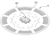
도 2는 일실시예에 적용된 프로브 카드의 저면도
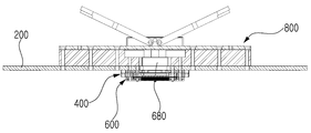
도 3은 일실시예에 적용된 프로브 카드의 측면 단면도
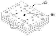
도 4는 도 1의 일부 확대도이다.
도 5는 일실시예에 적용된 종래 프로브 카드를 개략적으로 나타낸 측면 단면도
도 6은 일실시예에 따른 프로브 카드를 개략적으로 나타낸 측면 단면도
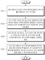
도 7은 일실시예에 따른 도 6의 프로브 카드의 동작을 순서대로 도시한 플로우 챠트
10: 프로브 카드
200: 프로브 기판 210: 내부배선
220 : 전극 230: 릴레이
400: 공간 변환기 410: 전극
420 : 내부배선 430: 릴레이
600: 프로브 헤드 620: 상부 플레이트
640: 하부 플레이트
Claims (4)
- 프로브 기판, 프로브 기판의 하부에 결합되는 공간 변환기 및 공간 변환기 하부에 결합되어 반도체 소자에 접촉하는 프로브 핀이 구비된 프로브 헤드를 포함하는 프로브 카드에 있어서,
상기 공간 변환기는,
상기 프로브 기판의 하부에 결합되고 복수의 홀이 형성되는 서브 기판;
상기 프로브 기판의 신호 송/수신에 대응하여 쌍으로 구비되는 채널의 전극에 대응하여 채널별로 구비되어서, 반도체 소자의 검사를 위한 단자가 되도록 하는 다수의 전극; 및
상기 반도체 소자가 검사될 시, 상기 프로브 기판 상의 단자 간 간격과 상기 프로브 핀 간의 간격의 차이를 보상하도록 프로브 핀의 상부와 연결하는 내부배선을 포함하되,
상기 공간 변환기는 상기 반도체 소자가 검사될 시, 상기 전극을 채널별로 쌍으로서 상호 간에 연결하도록 릴레이를 포함해서 상기 릴레이를 통해 임베디드 루프-백이 되도록 하는 것을 특징으로 하는 프로브 카드. - 제1항에 있어서,
상기 릴레이는
반도체 소자가 검사될 시, 반도체소자 검사의 싸이클 단위로 상이하게 구분해서 미리 설정된 채널을 대응되는 채널군별로 통합적으로 그룹핑해서 연결하므로 반도체소자 검사시의 채널단위로 통합적으로 임베디드 루프-백이 되는 것을 특징으로 하는 프로브 카드. - 프로브 기판, 프로브 기판의 하부에 결합되는 공간 변환기 및 공간 변환기 하부에 결합되어 반도체 소자에 접촉하는 프로브 핀이 구비된 프로브 헤드를 포함하는 프로브 카드에 있어서,
상기 공간 변환기는,
프로브 기판의 하부에 결합되고 복수의 제1홀이 형성되는 서브 기판; 및
상기 서브 기판에 형성된 제1홀에 결합되는 복수의 전도성 로드를 포함하고,
상기 전도성 로드는 상부가 프로브 기판에 형성된 채널과 전기적으로 연결되고, 하부는 프로브 핀의 상부와 연결되되,
상기 공간 변환기는 반도체 소자가 검사될 시, 상기 복수의 전도성 로드를 채널별로 쌍으로서 상호 간에 연결하도록 설치된 릴레이를 포함해서 상기 릴레이를 통해 임베디드 루프-백이 되도록 하는 것을 특징으로 하는 프로브 카드. - 제 3 항에 있어서,
상기 릴레이는
반도체 소자가 검사될 시, 반도체소자 검사의 싸이클 단위로 상이하게 구분해서 미리 설정된 채널을 대응되는 채널군별로 통합적으로 그룹핑해서 연결하므로 반도체소자 검사시의 채널단위로 통합적으로 임베디드 루프-백이 되는 것을 특징으로 하는 프로브 카드.
Applications Claiming Priority (2)
| Application Number | Priority Date | Filing Date | Title |
|---|---|---|---|
| KR20180148653 | 2018-11-27 | ||
| KR1020180148653 | 2018-11-27 |
Publications (2)
| Publication Number | Publication Date |
|---|---|
| KR20200063009A true KR20200063009A (ko) | 2020-06-04 |
| KR102148840B1 KR102148840B1 (ko) | 2020-08-28 |
Family
ID=71081186
Family Applications (1)
| Application Number | Title | Priority Date | Filing Date |
|---|---|---|---|
| KR1020190013840A Active KR102148840B1 (ko) | 2018-11-27 | 2019-02-01 | 프로브 카드 |
Country Status (1)
| Country | Link |
|---|---|
| KR (1) | KR102148840B1 (ko) |
Cited By (6)
| Publication number | Priority date | Publication date | Assignee | Title |
|---|---|---|---|---|
| KR102201929B1 (ko) * | 2019-10-11 | 2021-01-12 | 스테코 주식회사 | 프로브 카드 |
| US11437196B2 (en) * | 2019-01-31 | 2022-09-06 | Point Engineering Co., Ltd. | Multilayer ceramic substrate and probe card including same |
| KR20240080483A (ko) * | 2022-11-30 | 2024-06-07 | 주식회사 디오리진 | 프로브 카드, 프로브 카드를 포함한 테스트 장치, 그 프로브 카드를 이용한 테스트 방법 |
| KR20240175701A (ko) | 2023-06-13 | 2024-12-20 | 가부시키가이샤 니혼 마이크로닉스 | 릴레이 회로 및 전기적 접속 장치 |
| KR20240178228A (ko) | 2023-06-21 | 2024-12-30 | 가부시키가이샤 니혼 마이크로닉스 | 전기적 접속 장치 |
| KR102761296B1 (ko) * | 2023-11-24 | 2025-02-03 | 주식회사 비이링크 | 고전압-고전류용 전력반도체용 프로브 카드 |
Citations (8)
| Publication number | Priority date | Publication date | Assignee | Title |
|---|---|---|---|---|
| JP2007201471A (ja) * | 1998-12-31 | 2007-08-09 | Formfactor Inc | 半導体製品ダイのテスト方法及び同テストのためのテストダイを含むアセンブリ |
| KR20090018714A (ko) * | 2006-06-06 | 2009-02-20 | 폼팩터, 인코포레이티드 | 테스터기 구동 및 측정 성능을 확장하는 방법 |
| KR20100018181A (ko) * | 2008-08-06 | 2010-02-17 | 윌테크놀러지(주) | 프로브와 이를 포함하는 프로브 카드 |
| JP2014515095A (ja) * | 2011-03-16 | 2014-06-26 | フォームファクター, インコーポレイテッド | 無線プローブカード検証システム及び方法 |
| CN104297536A (zh) * | 2013-07-15 | 2015-01-21 | 旺矽科技股份有限公司 | 具回馈测试功能的探针模块 |
| KR101485994B1 (ko) * | 2014-01-27 | 2015-01-27 | 솔브레인이엔지 주식회사 | 수직형 프로브카드를 위한 효율적 공간변환기 |
| JP2017528713A (ja) * | 2014-08-29 | 2017-09-28 | アール アンド ディー サーキッツ インコーポレイテッドR & D Circuits Inc. | プリント回路基板内で被試験装置の直下に存在する埋込みシリアルデータ試験ループバックを実装する構造および実行方法 |
| KR20170112769A (ko) | 2016-04-01 | 2017-10-12 | 주식회사 에스디에이 | 프로브 카드 |
-
2019
- 2019-02-01 KR KR1020190013840A patent/KR102148840B1/ko active Active
Patent Citations (8)
| Publication number | Priority date | Publication date | Assignee | Title |
|---|---|---|---|---|
| JP2007201471A (ja) * | 1998-12-31 | 2007-08-09 | Formfactor Inc | 半導体製品ダイのテスト方法及び同テストのためのテストダイを含むアセンブリ |
| KR20090018714A (ko) * | 2006-06-06 | 2009-02-20 | 폼팩터, 인코포레이티드 | 테스터기 구동 및 측정 성능을 확장하는 방법 |
| KR20100018181A (ko) * | 2008-08-06 | 2010-02-17 | 윌테크놀러지(주) | 프로브와 이를 포함하는 프로브 카드 |
| JP2014515095A (ja) * | 2011-03-16 | 2014-06-26 | フォームファクター, インコーポレイテッド | 無線プローブカード検証システム及び方法 |
| CN104297536A (zh) * | 2013-07-15 | 2015-01-21 | 旺矽科技股份有限公司 | 具回馈测试功能的探针模块 |
| KR101485994B1 (ko) * | 2014-01-27 | 2015-01-27 | 솔브레인이엔지 주식회사 | 수직형 프로브카드를 위한 효율적 공간변환기 |
| JP2017528713A (ja) * | 2014-08-29 | 2017-09-28 | アール アンド ディー サーキッツ インコーポレイテッドR & D Circuits Inc. | プリント回路基板内で被試験装置の直下に存在する埋込みシリアルデータ試験ループバックを実装する構造および実行方法 |
| KR20170112769A (ko) | 2016-04-01 | 2017-10-12 | 주식회사 에스디에이 | 프로브 카드 |
Non-Patent Citations (3)
| Title |
|---|
| 그래서, 이러한 추세에 맞추어 30um 이하의 파인-피치 등의 반도체 소자 검사에 적용 가능한 프로브 카드를 개발할 필요가 있다. |
| 그리고, 한편 본 출원인은 이러한 상황을 배경으로 해서, 그러한 반도체 소자의 불량을 검사하기 위한 프로브 카드에서 임피던스 매칭이 가능하도록 새로운 기술 내용을 개발하였었다. |
| 또한, 다른 한편으로 최근에는 시스템화된 대규모 집적회로(System Large Scale Integration : System LSI) 제품의 속도, 다기능 보유 등의 성능 고도화에 따라 테스트의 중요성이 대두되고 있다. 그리고, 이에 더하여 새로운 설계/공정 개발 등으로 칩 사이즈는 점점 작아지고, 이에 대응하여 30um 이하의 파인-피치가 출현하고, 패드 사이즈 역시 작아지는 추세이다. |
Cited By (6)
| Publication number | Priority date | Publication date | Assignee | Title |
|---|---|---|---|---|
| US11437196B2 (en) * | 2019-01-31 | 2022-09-06 | Point Engineering Co., Ltd. | Multilayer ceramic substrate and probe card including same |
| KR102201929B1 (ko) * | 2019-10-11 | 2021-01-12 | 스테코 주식회사 | 프로브 카드 |
| KR20240080483A (ko) * | 2022-11-30 | 2024-06-07 | 주식회사 디오리진 | 프로브 카드, 프로브 카드를 포함한 테스트 장치, 그 프로브 카드를 이용한 테스트 방법 |
| KR20240175701A (ko) | 2023-06-13 | 2024-12-20 | 가부시키가이샤 니혼 마이크로닉스 | 릴레이 회로 및 전기적 접속 장치 |
| KR20240178228A (ko) | 2023-06-21 | 2024-12-30 | 가부시키가이샤 니혼 마이크로닉스 | 전기적 접속 장치 |
| KR102761296B1 (ko) * | 2023-11-24 | 2025-02-03 | 주식회사 비이링크 | 고전압-고전류용 전력반도체용 프로브 카드 |
Also Published As
| Publication number | Publication date |
|---|---|
| KR102148840B1 (ko) | 2020-08-28 |
Similar Documents
| Publication | Publication Date | Title |
|---|---|---|
| KR102148840B1 (ko) | 프로브 카드 | |
| KR101384714B1 (ko) | 반도체 검사장치 | |
| KR100385963B1 (ko) | 반도체 검사장치 및 이를 이용한 반도체장치 제조방법 | |
| KR101121644B1 (ko) | 프로브 카드용 공간 변환기 및 공간 변환기의 복구 방법 | |
| KR101045671B1 (ko) | 공간 변환기를 포함하는 프로브 카드 | |
| US20080175080A1 (en) | Semiconductor memory device and test method thereof | |
| KR100712561B1 (ko) | 웨이퍼 형태의 프로브 카드 및 그 제조방법과 웨이퍼형태의 프로브 카드를 구비한 반도체 검사장치 | |
| KR101980865B1 (ko) | 프로브 카드 | |
| KR20100069300A (ko) | 프로브 카드와, 이를 이용한 반도체 디바이스 테스트 장치 및 방법 | |
| CN207457425U (zh) | 基于微机电探针的垂直式探针卡 | |
| KR100683444B1 (ko) | 프로브 카드의 기판 및 그 기판의 재생 방법 | |
| KR102093419B1 (ko) | 프로브 카드 | |
| KR100448528B1 (ko) | 반도체장치의 검사장치 및 그를 이용한 반도체제조방법 | |
| KR100643842B1 (ko) | 마이크로핀이 인터페이스 보드에 삽입되는 프로브 장치 | |
| KR101391794B1 (ko) | 프로브 유닛 및 프로브 카드 | |
| KR20190061647A (ko) | 프로브 카드용 공간 변환기 및 그 제조방법 | |
| JP2005315775A (ja) | 片面移動式プローブを用いた4端子検査方法及び4端子検査用治具 | |
| KR101467381B1 (ko) | 반도체 검사장치 | |
| KR101434962B1 (ko) | 분기기판을 포함하는 프로브 카드 | |
| KR20090075515A (ko) | 프로브 카드 및 이를 포함하는 테스트 장비 | |
| KR100480665B1 (ko) | 수직식 프로브 장치 | |
| TW202316129A (zh) | 晶片檢測裝置 | |
| JP2003084040A (ja) | 半導体検査装置の製造方法および半導体検査装置 | |
| CN223377437U (zh) | 测试装置 | |
| KR200381448Y1 (ko) | 마이크로핀이 인터페이스 보드에 삽입되는 프로브 장치 |
Legal Events
| Date | Code | Title | Description |
|---|---|---|---|
| A201 | Request for examination | ||
| PA0109 | Patent application |
Patent event code: PA01091R01D Comment text: Patent Application Patent event date: 20190201 |
|
| PA0201 | Request for examination | ||
| E902 | Notification of reason for refusal | ||
| PE0902 | Notice of grounds for rejection |
Comment text: Notification of reason for refusal Patent event date: 20200111 Patent event code: PE09021S01D |
|
| E701 | Decision to grant or registration of patent right | ||
| PE0701 | Decision of registration |
Patent event code: PE07011S01D Comment text: Decision to Grant Registration Patent event date: 20200520 |
|
| PG1501 | Laying open of application | ||
| GRNT | Written decision to grant | ||
| PR0701 | Registration of establishment |
Comment text: Registration of Establishment Patent event date: 20200821 Patent event code: PR07011E01D |
|
| PR1002 | Payment of registration fee |
Payment date: 20200824 End annual number: 3 Start annual number: 1 |
|
| PG1601 | Publication of registration | ||
| PR1001 | Payment of annual fee |
Payment date: 20240821 Start annual number: 5 End annual number: 5 |
|
| PR1001 | Payment of annual fee |
Payment date: 20250626 Start annual number: 6 End annual number: 6 |