KR20200063181A - 열적 관통 접속부를 포함한 인쇄회로기판의 제조 방법, 그리고 인쇄회로기판 - Google Patents
열적 관통 접속부를 포함한 인쇄회로기판의 제조 방법, 그리고 인쇄회로기판 Download PDFInfo
- Publication number
- KR20200063181A KR20200063181A KR1020207012018A KR20207012018A KR20200063181A KR 20200063181 A KR20200063181 A KR 20200063181A KR 1020207012018 A KR1020207012018 A KR 1020207012018A KR 20207012018 A KR20207012018 A KR 20207012018A KR 20200063181 A KR20200063181 A KR 20200063181A
- Authority
- KR
- South Korea
- Prior art keywords
- solder
- solder resist
- thermal
- bore holes
- printed circuit
- Prior art date
- Legal status (The legal status is an assumption and is not a legal conclusion. Google has not performed a legal analysis and makes no representation as to the accuracy of the status listed.)
- Granted
Links
Images




Classifications
-
- H—ELECTRICITY
- H05—ELECTRIC TECHNIQUES NOT OTHERWISE PROVIDED FOR
- H05K—PRINTED CIRCUITS; CASINGS OR CONSTRUCTIONAL DETAILS OF ELECTRIC APPARATUS; MANUFACTURE OF ASSEMBLAGES OF ELECTRICAL COMPONENTS
- H05K1/00—Printed circuits
- H05K1/02—Details
- H05K1/0201—Thermal arrangements, e.g. for cooling, heating or preventing overheating
- H05K1/0203—Cooling of mounted components
- H05K1/0204—Cooling of mounted components using means for thermal conduction connection in the thickness direction of the substrate
- H05K1/0206—Cooling of mounted components using means for thermal conduction connection in the thickness direction of the substrate by printed thermal vias
-
- H—ELECTRICITY
- H05—ELECTRIC TECHNIQUES NOT OTHERWISE PROVIDED FOR
- H05K—PRINTED CIRCUITS; CASINGS OR CONSTRUCTIONAL DETAILS OF ELECTRIC APPARATUS; MANUFACTURE OF ASSEMBLAGES OF ELECTRICAL COMPONENTS
- H05K1/00—Printed circuits
- H05K1/02—Details
- H05K1/11—Printed elements for providing electric connections to or between printed circuits
- H05K1/111—Pads for surface mounting, e.g. lay-out
- H05K1/112—Pads for surface mounting, e.g. lay-out directly combined with via connections
- H05K1/113—Via provided in pad; Pad over filled via
-
- H—ELECTRICITY
- H05—ELECTRIC TECHNIQUES NOT OTHERWISE PROVIDED FOR
- H05K—PRINTED CIRCUITS; CASINGS OR CONSTRUCTIONAL DETAILS OF ELECTRIC APPARATUS; MANUFACTURE OF ASSEMBLAGES OF ELECTRICAL COMPONENTS
- H05K3/00—Apparatus or processes for manufacturing printed circuits
- H05K3/0094—Filling or covering plated through-holes or blind plated vias, e.g. for masking or for mechanical reinforcement
-
- H—ELECTRICITY
- H05—ELECTRIC TECHNIQUES NOT OTHERWISE PROVIDED FOR
- H05K—PRINTED CIRCUITS; CASINGS OR CONSTRUCTIONAL DETAILS OF ELECTRIC APPARATUS; MANUFACTURE OF ASSEMBLAGES OF ELECTRICAL COMPONENTS
- H05K3/00—Apparatus or processes for manufacturing printed circuits
- H05K3/30—Assembling printed circuits with electric components, e.g. with resistors
- H05K3/32—Assembling printed circuits with electric components, e.g. with resistors electrically connecting electric components or wires to printed circuits
- H05K3/34—Assembling printed circuits with electric components, e.g. with resistors electrically connecting electric components or wires to printed circuits by soldering
- H05K3/341—Surface mounted components
-
- H—ELECTRICITY
- H05—ELECTRIC TECHNIQUES NOT OTHERWISE PROVIDED FOR
- H05K—PRINTED CIRCUITS; CASINGS OR CONSTRUCTIONAL DETAILS OF ELECTRIC APPARATUS; MANUFACTURE OF ASSEMBLAGES OF ELECTRICAL COMPONENTS
- H05K3/00—Apparatus or processes for manufacturing printed circuits
- H05K3/30—Assembling printed circuits with electric components, e.g. with resistors
- H05K3/32—Assembling printed circuits with electric components, e.g. with resistors electrically connecting electric components or wires to printed circuits
- H05K3/34—Assembling printed circuits with electric components, e.g. with resistors electrically connecting electric components or wires to printed circuits by soldering
- H05K3/3452—Solder masks
-
- H—ELECTRICITY
- H05—ELECTRIC TECHNIQUES NOT OTHERWISE PROVIDED FOR
- H05K—PRINTED CIRCUITS; CASINGS OR CONSTRUCTIONAL DETAILS OF ELECTRIC APPARATUS; MANUFACTURE OF ASSEMBLAGES OF ELECTRICAL COMPONENTS
- H05K3/00—Apparatus or processes for manufacturing printed circuits
- H05K3/40—Forming printed elements for providing electric connections to or between printed circuits
- H05K3/42—Plated through-holes or plated via connections
-
- H—ELECTRICITY
- H05—ELECTRIC TECHNIQUES NOT OTHERWISE PROVIDED FOR
- H05K—PRINTED CIRCUITS; CASINGS OR CONSTRUCTIONAL DETAILS OF ELECTRIC APPARATUS; MANUFACTURE OF ASSEMBLAGES OF ELECTRICAL COMPONENTS
- H05K1/00—Printed circuits
- H05K1/02—Details
- H05K1/11—Printed elements for providing electric connections to or between printed circuits
- H05K1/111—Pads for surface mounting, e.g. lay-out
- H05K1/112—Pads for surface mounting, e.g. lay-out directly combined with via connections
-
- H—ELECTRICITY
- H05—ELECTRIC TECHNIQUES NOT OTHERWISE PROVIDED FOR
- H05K—PRINTED CIRCUITS; CASINGS OR CONSTRUCTIONAL DETAILS OF ELECTRIC APPARATUS; MANUFACTURE OF ASSEMBLAGES OF ELECTRICAL COMPONENTS
- H05K2201/00—Indexing scheme relating to printed circuits covered by H05K1/00
- H05K2201/09—Shape and layout
- H05K2201/09209—Shape and layout details of conductors
- H05K2201/09372—Pads and lands
- H05K2201/09481—Via in pad; Pad over filled via
-
- H—ELECTRICITY
- H05—ELECTRIC TECHNIQUES NOT OTHERWISE PROVIDED FOR
- H05K—PRINTED CIRCUITS; CASINGS OR CONSTRUCTIONAL DETAILS OF ELECTRIC APPARATUS; MANUFACTURE OF ASSEMBLAGES OF ELECTRICAL COMPONENTS
- H05K2201/00—Indexing scheme relating to printed circuits covered by H05K1/00
- H05K2201/09—Shape and layout
- H05K2201/09209—Shape and layout details of conductors
- H05K2201/095—Conductive through-holes or vias
- H05K2201/09563—Metal filled via
-
- H—ELECTRICITY
- H05—ELECTRIC TECHNIQUES NOT OTHERWISE PROVIDED FOR
- H05K—PRINTED CIRCUITS; CASINGS OR CONSTRUCTIONAL DETAILS OF ELECTRIC APPARATUS; MANUFACTURE OF ASSEMBLAGES OF ELECTRICAL COMPONENTS
- H05K2201/00—Indexing scheme relating to printed circuits covered by H05K1/00
- H05K2201/09—Shape and layout
- H05K2201/09209—Shape and layout details of conductors
- H05K2201/095—Conductive through-holes or vias
- H05K2201/09572—Solder filled plated through-hole in the final product
-
- H—ELECTRICITY
- H05—ELECTRIC TECHNIQUES NOT OTHERWISE PROVIDED FOR
- H05K—PRINTED CIRCUITS; CASINGS OR CONSTRUCTIONAL DETAILS OF ELECTRIC APPARATUS; MANUFACTURE OF ASSEMBLAGES OF ELECTRICAL COMPONENTS
- H05K2201/00—Indexing scheme relating to printed circuits covered by H05K1/00
- H05K2201/09—Shape and layout
- H05K2201/09209—Shape and layout details of conductors
- H05K2201/095—Conductive through-holes or vias
- H05K2201/09609—Via grid, i.e. two-dimensional array of vias or holes in a single plane
-
- H—ELECTRICITY
- H05—ELECTRIC TECHNIQUES NOT OTHERWISE PROVIDED FOR
- H05K—PRINTED CIRCUITS; CASINGS OR CONSTRUCTIONAL DETAILS OF ELECTRIC APPARATUS; MANUFACTURE OF ASSEMBLAGES OF ELECTRICAL COMPONENTS
- H05K2201/00—Indexing scheme relating to printed circuits covered by H05K1/00
- H05K2201/09—Shape and layout
- H05K2201/09209—Shape and layout details of conductors
- H05K2201/095—Conductive through-holes or vias
- H05K2201/09627—Special connections between adjacent vias, not for grounding vias
-
- H—ELECTRICITY
- H05—ELECTRIC TECHNIQUES NOT OTHERWISE PROVIDED FOR
- H05K—PRINTED CIRCUITS; CASINGS OR CONSTRUCTIONAL DETAILS OF ELECTRIC APPARATUS; MANUFACTURE OF ASSEMBLAGES OF ELECTRICAL COMPONENTS
- H05K2201/00—Indexing scheme relating to printed circuits covered by H05K1/00
- H05K2201/09—Shape and layout
- H05K2201/09209—Shape and layout details of conductors
- H05K2201/095—Conductive through-holes or vias
- H05K2201/09636—Details of adjacent, not connected vias
-
- H—ELECTRICITY
- H05—ELECTRIC TECHNIQUES NOT OTHERWISE PROVIDED FOR
- H05K—PRINTED CIRCUITS; CASINGS OR CONSTRUCTIONAL DETAILS OF ELECTRIC APPARATUS; MANUFACTURE OF ASSEMBLAGES OF ELECTRICAL COMPONENTS
- H05K2203/00—Indexing scheme relating to apparatus or processes for manufacturing printed circuits covered by H05K3/00
- H05K2203/04—Soldering or other types of metallurgic bonding
- H05K2203/043—Reflowing of solder coated conductors, not during connection of components, e.g. reflowing solder paste
-
- H—ELECTRICITY
- H05—ELECTRIC TECHNIQUES NOT OTHERWISE PROVIDED FOR
- H05K—PRINTED CIRCUITS; CASINGS OR CONSTRUCTIONAL DETAILS OF ELECTRIC APPARATUS; MANUFACTURE OF ASSEMBLAGES OF ELECTRICAL COMPONENTS
- H05K2203/00—Indexing scheme relating to apparatus or processes for manufacturing printed circuits covered by H05K3/00
- H05K2203/04—Soldering or other types of metallurgic bonding
- H05K2203/045—Solder-filled plated through-hole [PTH] during processing wherein the solder is removed from the PTH after processing
-
- H—ELECTRICITY
- H05—ELECTRIC TECHNIQUES NOT OTHERWISE PROVIDED FOR
- H05K—PRINTED CIRCUITS; CASINGS OR CONSTRUCTIONAL DETAILS OF ELECTRIC APPARATUS; MANUFACTURE OF ASSEMBLAGES OF ELECTRICAL COMPONENTS
- H05K2203/00—Indexing scheme relating to apparatus or processes for manufacturing printed circuits covered by H05K3/00
- H05K2203/04—Soldering or other types of metallurgic bonding
- H05K2203/0455—PTH for surface mount device [SMD], e.g. wherein solder flows through the PTH during mounting
-
- H—ELECTRICITY
- H05—ELECTRIC TECHNIQUES NOT OTHERWISE PROVIDED FOR
- H05K—PRINTED CIRCUITS; CASINGS OR CONSTRUCTIONAL DETAILS OF ELECTRIC APPARATUS; MANUFACTURE OF ASSEMBLAGES OF ELECTRICAL COMPONENTS
- H05K2203/00—Indexing scheme relating to apparatus or processes for manufacturing printed circuits covered by H05K3/00
- H05K2203/14—Related to the order of processing steps
- H05K2203/1476—Same or similar kind of process performed in phases, e.g. coarse patterning followed by fine patterning
Landscapes
- Engineering & Computer Science (AREA)
- Microelectronics & Electronic Packaging (AREA)
- Manufacturing & Machinery (AREA)
- Electric Connection Of Electric Components To Printed Circuits (AREA)
Abstract
Description
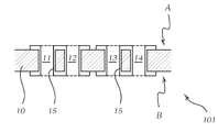
도 2는 솔더 레지스트 마스크들이 도포되어 있는 캐리어 플레이트를 도시한 도면이며, 더욱 정확하게 말하면 부분도 (a)는 캐리어 플레이트의 단면도이고, 부분도 (b)는 캐리어 플레이트의 하면의 상면도이다.
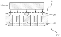
도 3은 솔더를 도포하고 리플로우 솔더링하는 단계를 도시한 도면이다.
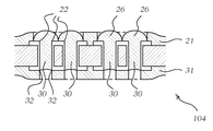
도 4는 리플로우 솔더링 단계를 통해 달성되어 캐리어 플레이트 내의 보어홀들이 충전되어 있는 상태를 도시한 상태도이다.
도 5는 앞서 캐리어 플레이트가 뒤집힌 조건에서, 상면에서 영역들을 노출시키는 후속 단계를 도시한 도면이다.
도 6은 캐리어 플레이트에 전자 부품들을 장착하는 추가 단계를 도시한 도면이다.
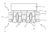
도 7은 그에 따라 수득된 인쇄회로기판을 도시한 도면이다.
도 8은 본 발명의 제2 실시형태에 따른, 솔더 레지스트 마스크들을 포함한 캐리어 플레이트를 도시한 도면이다.
Claims (13)
- 안쪽에 사전 형성된 복수의 보어홀(11, 12, 13, 14)을 포함하는 캐리어 플레이트(101)에서 출발하여 인쇄회로기판에서 열적 관통 접속부(19)들을 생성하기 위한 방법으로서, 복수의 보어홀은 캐리어 플레이트(101)의 하면(A)과 상면(B) 사이에 형성되고 각각 열적 관통 접속부들이 생성될 위치들에 위치되는, 상기 열적 관통 접속부의 생성 방법에 있어서, 상기 방법은,
- 상기 하면(A) 및 상기 상면(B) 상에 각각 제1 및 제2 솔더 레지스트 마스크(21, 31)를 도포하는 도포 단계이며, 상기 제1 솔더 레지스트 마스크(21)는 보어홀(11 ~ 14)들이 사전 형성된 조건에서 각각 상기 하면 상에서 각자의 보어홀의 테두리부(22)의 둘레에 솔더 레지스트가 없는 자유 영역(23)을 포함하며, 상기 제2 솔더 레지스트 마스크(31)는 적어도 대부분에서, 바람직하게는 상기 사전 형성된 보어홀(11 ~ 14)들 중 각자의 보어홀에서 각각 적어도 상기 상면 상의 보어홀의 테두리부(32)에까지 닿는, 상기 도포 단계;
- 상기 하면(A) 상에 솔더(16)를 도포하고 솔더를 리플로우 솔더링하는 도포 및 리플로우 솔더링 단계이며, 상기 솔더는 보어홀(11 ~ 14)들 내로 침투하여 하면(A) 상에서는 각각의 보어홀들의 테두리부(22)보다 더 돌출되는 볼록한 메니스커스(26)들을 형성하는, 도포 및 리플로우 솔더링 단계; 및
- 적어도 상기 상면 상에서 적어도 하나의 전자 부품(18)과 접촉하도록 기결정되어 있으면서 각각은 열적 관통 접속부들 중 적어도 하나를 포함하는 영역들에서 상기 제2 솔더 레지스트 마스크(31)를 제거하는 것을 통해, 상기 상면(B) 상에서 상기 영역(35)들을 노출시키는 노출 단계;를 포함하는 것을 특징으로 하는 열적 관통 접속부의 생성 방법. - 제1항에 있어서, 상기 제1 솔더 레지스트 마스크(21) 내에는 솔더 레지스트가 없는 자유 영역(23)들이 환형으로 형성되는 것을 특징으로 하는 열적 관통 접속부의 생성 방법.
- 제2항에 있어서, 직접 인접하는 보어홀들의 자유 영역들이면서 솔더 레지스트가 없는 상기 자유 영역(23)들은 상호 간에 접촉하며, 그럼으로써 상기 자유 영역들 사이에는 솔더 레지스트를 포함한 구역(25)들이 형성되며, 상기 구역들은 바람직하게는 오목한 곡선 세그먼트들에 의해 범위 한정되는 사각형 또는 삼각형의 형태를 보유하는 것을 특징으로 하는 열적 관통 접속부의 생성 방법.
- 제1항 내지 제3항 중 어느 한 항에 있어서, 상기 제2 솔더 레지스트 마스크(31)는 상기 보어홀들 중 적어도 일부분에서 테두리부(32) 위쪽에 도달하고 그곳에서 각각 독립해 있으면서 안쪽으로 돌출된 하나의 링(34)을 형성하는 것을 특징으로 하는 열적 관통 접속부의 생성 방법.
- 제1항 내지 제4항 중 어느 한 항에 있어서, 상기 제2 솔더 레지스트 마스크(31)는 상기 보어홀들 중 적어도 일부분에서 테두리부(32)에까지 닿으며, 상기 보어홀들에서 상기 제2 솔더 레지스트 마스크의 테두리부(33)는 상기 보어홀의 테두리부(32)와 동일 평면에 놓이는 것을 특징으로 하는 열적 관통 접속부의 생성 방법.
- 제1항 내지 제5항 중 어느 한 항에 있어서, 상기 캐리어 플레이트는 솔더를 도포하는 단계 동안 상기 하면(A)이 상부 방향으로 배향되어 파지되는 것을 특징으로 하는 열적 관통 접속부의 생성 방법.
- 제1항 내지 제6항 중 어느 한 항에 있어서, 그에 뒤이어 실행되는 추가 단계로서, 접촉을 위한 상기 노출된 영역(35)들에서 적어도 하나의 전자 부품(18)을 상기 상면(B)에 장착하는 추가 단계가 제공되는 것을 특징으로 하는 열적 관통 접속부의 생성 방법.
- 제1항 내지 제7항 중 어느 한 항에 있어서, 상기 하면(A) 상에서 솔더의 리플로우 솔더링 단계 동안 발생하는 메니스커스(26)들은 각각 보어홀들 위쪽에 볼록한 구면을 형성하는 것을 특징으로 하는 열적 관통 접속부의 생성 방법.
- 제1항 내지 제8항 중 어느 한 항에 있어서, 사전에 실행되는 추가 단계로서,
- 금속으로, 바람직하게는 예컨대 구리처럼 높은 전기 전도도를 갖는 금속으로, 그리고 바람직하게는 갈바닉 방법을 통해, 상기 사전 형성된 보어홀(11 ~ 14)들을 라이닝하는 상기 추가 단계가 제공되는 것을 특징으로 하는 열적 관통 접속부의 생성 방법. - 제1항 내지 제9항 중 어느 한 항에 있어서, 솔더의 리플로우 솔더링 단계 동안, 상기 솔더(16)가 그 내로 침투하는 상기 보어홀(11 ~ 14)들은 상기 솔더(16)를 통해 충전되는 것을 특징으로 하는 열적 관통 접속부의 생성 방법.
- 인쇄회로기판의 캐리어 플레이트(10) 내에 형성된 복수의 관통 접속부(19)를 포함한 인쇄회로기판(1)으로서, 상기 관통 접속부들은 캐리어 플레이트(10)의 하면(A)과 상면(B) 사이에 형성되는 보어홀(20)들을 따라서 연장되는, 상기 인쇄회로기판에 있어서,
상기 하면(A) 상의 상기 열적 관통 접속부들은 각각의 보어홀(20)들이 테두리부보다 더 돌출되는 볼록한 메니스커스(26)들을 포함하며, 그리고
상기 상면(B) 상에는 솔더 레지스트 마스크(37)가 제거된 영역(35)들이 제공되며, 상기 영역(35)들에는 상기 상면 상에서 적어도 하나의 전자 부품(18)과 접촉하기 위한 솔더 재료가 마련되며, 그리고 상기 영역들은 열적 관통 접속부(19)들 중 적어도 하나와 솔더로 연결되는 것을 특징으로 하는 인쇄회로기판. - 제11항에 있어서, 상기 하면(A) 상에서 상기 메니스커스(26)들은 원형이며, 그리고 바람직하게는 직접 인접한 보어홀들의 메니스커스(26)들은 상호 간에 접촉하며, 상기 메니스커스들 사이에는 각각 솔더 레지스트를 포함한 구역(25)들이 위치하고, 상기 구역들은 바람직하게는 오목한 곡선 세그먼트들을 통해 범위 한정되는 사각형 또는 삼각형의 형태를 보유하는 것을 특징으로 하는 인쇄회로기판.
- 제11항 또는 제12항에 있어서, 상기 메니스커스(26)들은 솔더 재료(16)를 통해 형성되며, 상기 솔더 재료는 그와 동시에 상기 보어홀(20)들을 충전하는 것을 특징으로 하는 인쇄회로기판.
Applications Claiming Priority (3)
| Application Number | Priority Date | Filing Date | Title |
|---|---|---|---|
| ATA50871/2017A AT520301B1 (de) | 2017-10-12 | 2017-10-12 | Verfahren zum erzeugen einer leiterplatte mit thermischen durchkontaktierungen, sowie leiterplatte |
| ATA50871/2017 | 2017-10-12 | ||
| PCT/AT2018/060235 WO2019071283A1 (de) | 2017-10-12 | 2018-10-08 | Verfahren zum erzeugen einer leiterplatte mit thermischen durchkontaktierungen, sowie leiterplatte |
Publications (2)
| Publication Number | Publication Date |
|---|---|
| KR20200063181A true KR20200063181A (ko) | 2020-06-04 |
| KR102416156B1 KR102416156B1 (ko) | 2022-07-06 |
Family
ID=63861945
Family Applications (1)
| Application Number | Title | Priority Date | Filing Date |
|---|---|---|---|
| KR1020207012018A Active KR102416156B1 (ko) | 2017-10-12 | 2018-10-08 | 열적 관통 접속부를 포함한 인쇄회로기판의 제조 방법, 그리고 인쇄회로기판 |
Country Status (7)
| Country | Link |
|---|---|
| US (1) | US11116071B2 (ko) |
| EP (1) | EP3695691B1 (ko) |
| JP (1) | JP6953630B2 (ko) |
| KR (1) | KR102416156B1 (ko) |
| CN (1) | CN111201840B (ko) |
| AT (1) | AT520301B1 (ko) |
| WO (1) | WO2019071283A1 (ko) |
Families Citing this family (5)
| Publication number | Priority date | Publication date | Assignee | Title |
|---|---|---|---|---|
| EP3745828B1 (en) * | 2019-05-28 | 2022-11-09 | Mitsubishi Electric R&D Centre Europe B.V. | Method of forming high density vias in a multilayer substrate |
| DE102021114658A1 (de) | 2021-06-08 | 2022-12-08 | Continental Automotive Gmbh | Leiterplatte für ein Leistungshalbleitermodul, Leistungshalbleitermodul sowie Verfahren zur Herstellung einer Leiterplatte und eines Leistungshalbleitermoduls |
| DE102021117131A1 (de) * | 2021-07-02 | 2023-01-05 | Lisa Dräxlmaier GmbH | Leiterplatte und verfahren zum prozesssicheren auflöten eines chipgehäuses |
| US20240090756A1 (en) * | 2022-09-16 | 2024-03-21 | Karl Storz Endovision, Inc. | Endoscopic System with Electrical Bridge in Distal Tip |
| JP2024077401A (ja) * | 2022-11-28 | 2024-06-07 | オムロン株式会社 | 基板 |
Citations (2)
| Publication number | Priority date | Publication date | Assignee | Title |
|---|---|---|---|---|
| JPH04336451A (ja) * | 1991-05-14 | 1992-11-24 | Fujitsu Ltd | 半導体チップの実装構造 |
| JP2006216901A (ja) * | 2005-02-07 | 2006-08-17 | Sharp Corp | プリント配線基板及び該プリント配線基板の部品実装方法 |
Family Cites Families (14)
| Publication number | Priority date | Publication date | Assignee | Title |
|---|---|---|---|---|
| US4396936A (en) * | 1980-12-29 | 1983-08-02 | Honeywell Information Systems, Inc. | Integrated circuit chip package with improved cooling means |
| GB8324839D0 (en) * | 1983-09-16 | 1983-10-19 | Lucas Ind Plc | Mounting carrier for microelectronic silicon chip |
| JPH01211992A (ja) | 1988-02-19 | 1989-08-25 | Hitachi Ltd | プリント基板用ソルダレジスト |
| US5129142A (en) * | 1990-10-30 | 1992-07-14 | International Business Machines Corporation | Encapsulated circuitized power core alignment and lamination |
| KR950012658B1 (ko) * | 1992-07-24 | 1995-10-19 | 삼성전자주식회사 | 반도체 칩 실장방법 및 기판 구조체 |
| DE19842590A1 (de) * | 1998-09-17 | 2000-04-13 | Daimler Chrysler Ag | Verfahren zur Herstellung von Schaltungsanordnungen |
| DE19909505C2 (de) | 1999-03-04 | 2001-11-15 | Daimler Chrysler Ag | Verfahren zur Herstellung von Schaltungsanordnungen |
| DE10101359A1 (de) | 2001-01-13 | 2002-07-25 | Conti Temic Microelectronic | Verfahren zur Herstellung einer elektronischen Baugruppe |
| GB0400982D0 (en) * | 2004-01-16 | 2004-02-18 | Fujifilm Electronic Imaging | Method of forming a pattern on a substrate |
| US7300857B2 (en) * | 2004-09-02 | 2007-11-27 | Micron Technology, Inc. | Through-wafer interconnects for photoimager and memory wafers |
| JP5142119B2 (ja) | 2006-09-20 | 2013-02-13 | 住友電装株式会社 | 放熱構造を備えたプリント基板の製造方法および該方法で製造されたプリント基板の放熱構造 |
| US8166650B2 (en) * | 2008-05-30 | 2012-05-01 | Steering Solutions IP Holding Company | Method of manufacturing a printed circuit board |
| TW201230897A (en) * | 2011-01-14 | 2012-07-16 | Askey Computer Corp | Circuit board |
| AT516724B1 (de) * | 2014-12-22 | 2016-08-15 | Zizala Lichtsysteme Gmbh | Herstellen einer schaltungsanordnung mit thermischen durchkontaktierungen |
-
2017
- 2017-10-12 AT ATA50871/2017A patent/AT520301B1/de active
-
2018
- 2018-10-08 EP EP18786659.5A patent/EP3695691B1/de active Active
- 2018-10-08 CN CN201880066243.1A patent/CN111201840B/zh active Active
- 2018-10-08 KR KR1020207012018A patent/KR102416156B1/ko active Active
- 2018-10-08 JP JP2020520461A patent/JP6953630B2/ja active Active
- 2018-10-08 US US16/754,693 patent/US11116071B2/en active Active
- 2018-10-08 WO PCT/AT2018/060235 patent/WO2019071283A1/de not_active Ceased
Patent Citations (2)
| Publication number | Priority date | Publication date | Assignee | Title |
|---|---|---|---|---|
| JPH04336451A (ja) * | 1991-05-14 | 1992-11-24 | Fujitsu Ltd | 半導体チップの実装構造 |
| JP2006216901A (ja) * | 2005-02-07 | 2006-08-17 | Sharp Corp | プリント配線基板及び該プリント配線基板の部品実装方法 |
Also Published As
| Publication number | Publication date |
|---|---|
| US11116071B2 (en) | 2021-09-07 |
| US20200236775A1 (en) | 2020-07-23 |
| JP6953630B2 (ja) | 2021-10-27 |
| JP2020537819A (ja) | 2020-12-24 |
| KR102416156B1 (ko) | 2022-07-06 |
| AT520301A4 (de) | 2019-03-15 |
| WO2019071283A1 (de) | 2019-04-18 |
| AT520301B1 (de) | 2019-03-15 |
| CN111201840B (zh) | 2023-06-02 |
| EP3695691B1 (de) | 2024-03-20 |
| CN111201840A (zh) | 2020-05-26 |
| EP3695691A1 (de) | 2020-08-19 |
Similar Documents
| Publication | Publication Date | Title |
|---|---|---|
| KR102416156B1 (ko) | 열적 관통 접속부를 포함한 인쇄회로기판의 제조 방법, 그리고 인쇄회로기판 | |
| US7606038B2 (en) | Method for producing a printed circuit board with a heat radiating structure and a printed circuit board with a heat radiating structure | |
| US4985601A (en) | Circuit boards with recessed traces | |
| US5055637A (en) | Circuit boards with recessed traces | |
| US8319116B2 (en) | Rib reinforcement of plated thru-holes | |
| CN105282969B (zh) | 印刷电路板及其制造方法 | |
| CN106973500A (zh) | 电子电路装置 | |
| CN103404244A (zh) | 印刷电路板及其制造方法 | |
| CN103681565B (zh) | 具有柱体的半导体封装基板及其相关方法 | |
| US7394159B2 (en) | Delamination reduction between vias and conductive pads | |
| US20200077515A1 (en) | Printed circuit board | |
| US8322596B2 (en) | Wiring substrate manufacturing method | |
| JP2009182229A (ja) | 配線回路基板およびその製造方法 | |
| JP2006294976A (ja) | 半導体装置およびその製造方法 | |
| JP5017872B2 (ja) | 半導体装置及びその製造方法 | |
| US7417312B2 (en) | Use of solder paste for heat dissipation | |
| CN112911797A (zh) | 用于制造导体结构元件的方法和导体结构元件 | |
| EP4629751A1 (en) | Substrate | |
| JP5573900B2 (ja) | 部品実装用基板及び部品実装構造体 | |
| TWI912745B (zh) | 基板及模組 | |
| JP4875844B2 (ja) | 半導体装置の製造方法 | |
| JP2007027341A (ja) | プリント配線板および電子部品実装構造 | |
| JPH11274704A (ja) | プリント配線基板 | |
| JP2020155694A (ja) | 両面配線基板 | |
| KR20150115346A (ko) | 인쇄회로기판 및 이의 제조 방법 |
Legal Events
| Date | Code | Title | Description |
|---|---|---|---|
| PA0105 | International application |
Patent event date: 20200424 Patent event code: PA01051R01D Comment text: International Patent Application |
|
| PA0201 | Request for examination | ||
| PG1501 | Laying open of application | ||
| E902 | Notification of reason for refusal | ||
| PE0902 | Notice of grounds for rejection |
Comment text: Notification of reason for refusal Patent event date: 20211007 Patent event code: PE09021S01D |
|
| E701 | Decision to grant or registration of patent right | ||
| PE0701 | Decision of registration |
Patent event code: PE07011S01D Comment text: Decision to Grant Registration Patent event date: 20220425 |
|
| GRNT | Written decision to grant | ||
| PR0701 | Registration of establishment |
Comment text: Registration of Establishment Patent event date: 20220629 Patent event code: PR07011E01D |
|
| PR1002 | Payment of registration fee |
Payment date: 20220630 End annual number: 3 Start annual number: 1 |
|
| PG1601 | Publication of registration |