KR20200063210A - 간섭계 스테이지 위치설정 장치 - Google Patents
간섭계 스테이지 위치설정 장치 Download PDFInfo
- Publication number
- KR20200063210A KR20200063210A KR1020207012683A KR20207012683A KR20200063210A KR 20200063210 A KR20200063210 A KR 20200063210A KR 1020207012683 A KR1020207012683 A KR 1020207012683A KR 20207012683 A KR20207012683 A KR 20207012683A KR 20200063210 A KR20200063210 A KR 20200063210A
- Authority
- KR
- South Korea
- Prior art keywords
- object table
- measurement
- axis
- sensor
- interferometer
- Prior art date
- Legal status (The legal status is an assumption and is not a legal conclusion. Google has not performed a legal analysis and makes no representation as to the accuracy of the status listed.)
- Granted
Links
- 238000005259 measurement Methods 0.000 claims abstract description 130
- 239000000758 substrate Substances 0.000 claims abstract description 60
- 238000007689 inspection Methods 0.000 claims abstract description 25
- 239000002245 particle Substances 0.000 claims description 34
- 238000000034 method Methods 0.000 claims description 17
- 230000006399 behavior Effects 0.000 claims description 6
- 238000012937 correction Methods 0.000 claims description 3
- 238000001459 lithography Methods 0.000 claims 1
- 238000010894 electron beam technology Methods 0.000 description 34
- 238000006073 displacement reaction Methods 0.000 description 26
- 230000003287 optical effect Effects 0.000 description 21
- 235000012431 wafers Nutrition 0.000 description 14
- 230000007547 defect Effects 0.000 description 9
- 239000004065 semiconductor Substances 0.000 description 9
- WFKWXMTUELFFGS-UHFFFAOYSA-N tungsten Chemical compound [W] WFKWXMTUELFFGS-UHFFFAOYSA-N 0.000 description 9
- 229910052721 tungsten Inorganic materials 0.000 description 9
- 239000010937 tungsten Substances 0.000 description 9
- 238000012986 modification Methods 0.000 description 5
- 230000004048 modification Effects 0.000 description 5
- 230000008569 process Effects 0.000 description 5
- MCMNRKCIXSYSNV-UHFFFAOYSA-N Zirconium dioxide Chemical compound O=[Zr]=O MCMNRKCIXSYSNV-UHFFFAOYSA-N 0.000 description 4
- 230000001133 acceleration Effects 0.000 description 4
- 238000003384 imaging method Methods 0.000 description 4
- 238000012545 processing Methods 0.000 description 3
- 230000004075 alteration Effects 0.000 description 2
- 239000000919 ceramic Substances 0.000 description 2
- 238000001352 electron-beam projection lithography Methods 0.000 description 2
- 239000000463 material Substances 0.000 description 2
- 238000012544 monitoring process Methods 0.000 description 2
- JBRZTFJDHDCESZ-UHFFFAOYSA-N AsGa Chemical compound [As]#[Ga] JBRZTFJDHDCESZ-UHFFFAOYSA-N 0.000 description 1
- 229910001218 Gallium arsenide Inorganic materials 0.000 description 1
- GPXJNWSHGFTCBW-UHFFFAOYSA-N Indium phosphide Chemical compound [In]#P GPXJNWSHGFTCBW-UHFFFAOYSA-N 0.000 description 1
- 230000004888 barrier function Effects 0.000 description 1
- 230000008901 benefit Effects 0.000 description 1
- 238000004891 communication Methods 0.000 description 1
- 238000009792 diffusion process Methods 0.000 description 1
- 230000005684 electric field Effects 0.000 description 1
- 230000005611 electricity Effects 0.000 description 1
- 238000000609 electron-beam lithography Methods 0.000 description 1
- 238000010438 heat treatment Methods 0.000 description 1
- 238000002955 isolation Methods 0.000 description 1
- 238000004519 manufacturing process Methods 0.000 description 1
- 229910021421 monocrystalline silicon Inorganic materials 0.000 description 1
- 238000012546 transfer Methods 0.000 description 1
- -1 two electrodes Substances 0.000 description 1
- 238000012795 verification Methods 0.000 description 1
Images


Classifications
-
- H—ELECTRICITY
- H01—ELECTRIC ELEMENTS
- H01J—ELECTRIC DISCHARGE TUBES OR DISCHARGE LAMPS
- H01J37/00—Discharge tubes with provision for introducing objects or material to be exposed to the discharge, e.g. for the purpose of examination or processing thereof
- H01J37/02—Details
- H01J37/20—Means for supporting or positioning the object or the material; Means for adjusting diaphragms or lenses associated with the support
-
- H—ELECTRICITY
- H01—ELECTRIC ELEMENTS
- H01J—ELECTRIC DISCHARGE TUBES OR DISCHARGE LAMPS
- H01J37/00—Discharge tubes with provision for introducing objects or material to be exposed to the discharge, e.g. for the purpose of examination or processing thereof
- H01J37/02—Details
- H01J37/244—Detectors; Associated components or circuits therefor
-
- H—ELECTRICITY
- H01—ELECTRIC ELEMENTS
- H01J—ELECTRIC DISCHARGE TUBES OR DISCHARGE LAMPS
- H01J37/00—Discharge tubes with provision for introducing objects or material to be exposed to the discharge, e.g. for the purpose of examination or processing thereof
- H01J37/30—Electron-beam or ion-beam tubes for localised treatment of objects
- H01J37/317—Electron-beam or ion-beam tubes for localised treatment of objects for changing properties of the objects or for applying thin layers thereon, e.g. for ion implantation
- H01J37/3174—Particle-beam lithography, e.g. electron beam lithography
-
- H—ELECTRICITY
- H01—ELECTRIC ELEMENTS
- H01J—ELECTRIC DISCHARGE TUBES OR DISCHARGE LAMPS
- H01J2237/00—Discharge tubes exposing object to beam, e.g. for analysis treatment, etching, imaging
- H01J2237/20—Positioning, supporting, modifying or maintaining the physical state of objects being observed or treated
- H01J2237/202—Movement
- H01J2237/20214—Rotation
-
- H—ELECTRICITY
- H01—ELECTRIC ELEMENTS
- H01J—ELECTRIC DISCHARGE TUBES OR DISCHARGE LAMPS
- H01J2237/00—Discharge tubes exposing object to beam, e.g. for analysis treatment, etching, imaging
- H01J2237/20—Positioning, supporting, modifying or maintaining the physical state of objects being observed or treated
- H01J2237/202—Movement
- H01J2237/20221—Translation
- H01J2237/20235—Z movement or adjustment
-
- H—ELECTRICITY
- H01—ELECTRIC ELEMENTS
- H01J—ELECTRIC DISCHARGE TUBES OR DISCHARGE LAMPS
- H01J2237/00—Discharge tubes exposing object to beam, e.g. for analysis treatment, etching, imaging
- H01J2237/20—Positioning, supporting, modifying or maintaining the physical state of objects being observed or treated
- H01J2237/202—Movement
- H01J2237/20292—Means for position and/or orientation registration
-
- H—ELECTRICITY
- H01—ELECTRIC ELEMENTS
- H01J—ELECTRIC DISCHARGE TUBES OR DISCHARGE LAMPS
- H01J2237/00—Discharge tubes exposing object to beam, e.g. for analysis treatment, etching, imaging
- H01J2237/245—Detection characterised by the variable being measured
- H01J2237/24571—Measurements of non-electric or non-magnetic variables
- H01J2237/24578—Spatial variables, e.g. position, distance
Landscapes
- Chemical & Material Sciences (AREA)
- Analytical Chemistry (AREA)
- Exposure And Positioning Against Photoresist Photosensitive Materials (AREA)
- Electron Beam Exposure (AREA)
- Testing Or Measuring Of Semiconductors Or The Like (AREA)
- Instruments For Measurement Of Length By Optical Means (AREA)
- Analysing Materials By The Use Of Radiation (AREA)
Abstract
Description
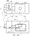
도 1a 및 도 1b는 본 발명의 일 실시예에 따른 e-빔 검사 툴의 개략적인 도면;
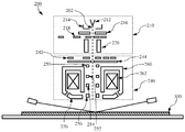
도 2 및 도 3은 본 발명의 일 실시예에서 적용될 수 있는 전자 광학 시스템의 개략적인 도면;
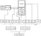
도 4는 본 발명에 따른 EBI 시스템의 가능한 제어 아키텍처를 개략적으로 도시하는 도면;
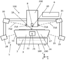
도 5는 본 발명의 일 실시예에 따른 e-빔 검사 툴의 제 1 실시예를 개략적으로 도시하는 도면;
도 6은 본 발명에 따른 대상물 테이블 상에 지지된 기판의 높이를 제어하기 위한 제어 방식을 개략적으로 도시하는 도면;
도 7은 본 발명의 일 실시예에 따른 e-빔 검사 툴의 제 2 실시예를 개략적으로 도시하는 도면;
도 8은 본 발명의 일 실시예에 따른 e-빔 검사 툴의 제 3 실시예를 개략적으로 도시하는 도면;
도 9는 본 발명의 일 실시예에 따른 e-빔 검사 툴의 제 4 실시예를 개략적으로 도시하는 도면이다.
Claims (15)
- 스테이지 장치로서,
지지 표면을 포함하는 대상물 테이블 -상기 대상물 테이블은 상기 지지 표면 상에 기판을 지지하도록 구성됨- ;
상기 대상물 테이블을 위치시키도록 구성되는 위치설정 디바이스;
제 1 축에 평행한 상기 대상물 테이블의 높이 위치를 측정하도록 구성되는 위치 센서를 포함하는 위치 측정 시스템 -상기 제 1 축은 상기 지지 표면에 실질적으로 수직이고, 상기 위치 센서는 간섭계 센서를 갖는 간섭계 측정 시스템을 포함함-
을 포함하며,
상기 간섭계 센서의 측정 빔은 측정 방향으로 상기 대상물 테이블의 반사 표면을 조사(irradiate)하도록 구성되고, 상기 측정 방향은 상기 제 1 축에 평행한 제 1 성분 및 제 2 축에 평행한 제 2 성분을 가지며, 상기 제 2 축은 상기 제 1 축에 실질적으로 수직인 스테이지 장치. - 제 1 항에 있어서,
상기 위치 측정 시스템은:
상기 제 1 축에 평행한 상기 기판의 추가 높이 위치를 측정하도록 구성되는 제 2 위치 센서;
작동 신호를 제공하는 제어기; 및
적어도 부분적으로 상기 작동 신호에 기초하여 상기 대상물 테이블의 높이 위치를 조정하도록 구성되는 적어도 하나의 액추에이터를 더 포함하고,
상기 스테이지 장치는 상기 위치 센서의 측정 속도에 비해 낮은 측정 속도에서의 상기 제 2 위치 센서를 사용하여 상기 기판의 추가 높이 위치를 측정하도록 구성되며,
상기 제어기는 마스터 제어 루프 및 슬레이브 제어 루프를 갖는 마스터-슬레이브 구성을 포함하고, 사용 시 상기 슬레이브 제어 루프에서 상기 위치 센서는 상기 기판의 추가 높이 위치를 제어하는 데 사용되고, 사용 시 상기 마스터 제어 루프에서 상기 제 2 위치 센서는 상기 슬레이브 제어 루프를 위한 설정점(set-point)을 제공하는 데 사용되는 스테이지 장치. - 제 1 항에 있어서,
상기 반사 표면은 상기 간섭계 센서의 측정 방향에 실질적으로 수직으로 배치되는 스테이지 장치. - 제 1 항에 있어서,
상기 측정 방향과 상기 제 2 축 사이의 각도는 2 내지 20 도인 스테이지 장치. - 제 1 항에 있어서,
상기 간섭계 센서의 기준 빔의 기준 빔 방향은 상기 측정 빔에 실질적으로 평행이거나, 또는 상기 제 2 축에 실질적으로 평행인 스테이지 장치. - 제 1 항에 있어서,
상기 기판을 지지하지 않는 대상물 테이블의 표면인 상기 대상물 테이블의 측표면이 상기 대상물 테이블의 반사 표면을 형성하도록 구성되거나, 또는 상기 대상물 테이블의 측표면에 장착된 반사 표면 요소가 상기 대상물 테이블의 반사 표면을 형성하도록 구성되는 스테이지 장치. - 제 1 항 또는 제 2 항에 있어서,
상기 위치 측정 시스템 및/또는 제어기는 상기 대상물 테이블의 반사 표면의 상이한 위치들에서의 반사 거동들의 차이들을 보정하도록 구성되는 상기 대상물 테이블의 반사 표면의 보정 맵(correction map)을 포함하는 스테이지 장치. - 제 1 항에 있어서,
상기 간섭계 측정 시스템은 제 2 간섭계 센서를 포함하며, 상기 제 2 간섭계 센서의 제 2 측정 빔은 제 2 측정 방향으로 상기 대상물 테이블의 제 2 반사 표면으로 지향되고, 상기 제 2 측정 방향은 상기 제 1 축에 평행한 제 3 성분 및 제 3 축에 평행한 제 4 성분을 가지며, 상기 제 3 축은 상기 제 1 축에 실질적으로 수직인 스테이지 장치. - 제 8 항에 있어서,
상기 반사 표면 및 상기 제 2 반사 표면은 상기 제 1 축에 대해 상기 대상물 테이블의 양측에 배치되고,
상기 측정 방향의 제 1 성분 및 상기 제 2 측정 방향의 제 3 성분은 동일한 방향을 갖고, 상기 측정 방향의 제 2 성분 및 상기 제 2 측정 방향의 제 4 성분은 반대 방향을 갖는 스테이지 장치. - 제 8 항에 있어서,
기준 빔 및 상기 제 2 간섭계 센서의 제 2 기준 빔은 실질적으로 동일한 길이를 갖는 스테이지 장치. - 제 8 항에 있어서,
상기 측정 빔의 측정 방향 및 상기 제 2 측정 빔의 제 2 측정 방향은 상기 기판 상의 타겟 위치에서 교차하는 스테이지 장치. - 입자 빔 장치로서,
기판에 입자 빔을 제공하도록 구성되는 입자 빔 발생기; 및
제 1 항에 따른 스테이지 장치
를 포함하고,
기준 빔에 의해 조사되도록 구성되는 간섭계 센서의 반사 기준 표면은 상기 입자 빔 발생기에 배치되는 입자 빔 장치. - 입자 빔 장치로서,
기판에 입자 빔을 제공하도록 구성되는 입자 빔 발생기; 및
제 1 항에 따른 스테이지 장치
를 포함하고,
반사 기준 표면은 상기 입자 빔 발생기를 지지하는 프레임에 배치되는 입자 빔 장치. - 입자 빔 장치로서,
기판에 입자 빔을 제공하도록 구성되는 입자 빔 발생기; 및
제 8 항에 따른 스테이지 장치
를 포함하고,
기준 빔 방향 및 제 2 기준 빔의 제 2 기준 빔 방향은 상기 입자 빔 발생기 상의 제 2 타겟 위치에서 교차하는 입자 빔 장치. - 제 1 항에 따른 스테이지 장치를 포함하는 장치로서,
상기 장치는 입자 빔 장치, e-빔 장치, e-빔 검사 장치, 리소그래피 장치, 메트롤로지 장치, 또는 진공 장치인 장치.
Applications Claiming Priority (3)
| Application Number | Priority Date | Filing Date | Title |
|---|---|---|---|
| EP17194665 | 2017-10-04 | ||
| EP17194665.0 | 2017-10-04 | ||
| PCT/EP2018/076571 WO2019068601A1 (en) | 2017-10-04 | 2018-10-01 | INTERFEROMETRIC PLATE PLATFORM POSITIONING APPARATUS |
Publications (2)
| Publication Number | Publication Date |
|---|---|
| KR20200063210A true KR20200063210A (ko) | 2020-06-04 |
| KR102520040B1 KR102520040B1 (ko) | 2023-04-10 |
Family
ID=60021937
Family Applications (1)
| Application Number | Title | Priority Date | Filing Date |
|---|---|---|---|
| KR1020207012683A Active KR102520040B1 (ko) | 2017-10-04 | 2018-10-01 | 간섭계 스테이지 위치설정 장치 |
Country Status (7)
| Country | Link |
|---|---|
| US (1) | US11476077B2 (ko) |
| JP (1) | JP7200234B2 (ko) |
| KR (1) | KR102520040B1 (ko) |
| CN (1) | CN111183501B (ko) |
| IL (1) | IL273651B2 (ko) |
| TW (1) | TWI729315B (ko) |
| WO (1) | WO2019068601A1 (ko) |
Cited By (1)
| Publication number | Priority date | Publication date | Assignee | Title |
|---|---|---|---|---|
| KR20240017400A (ko) * | 2021-06-07 | 2024-02-07 | 테크니쉐 유니버지탯 빈 | 시료 지지대의 위치 설정 동안 간섭 변수 보상을 위한 방법 및 장치 |
Families Citing this family (2)
| Publication number | Priority date | Publication date | Assignee | Title |
|---|---|---|---|---|
| WO2025223848A1 (en) | 2024-04-23 | 2025-10-30 | Carl Zeiss Smt Gmbh | Inspection apparatus for 3D tomography with improved stand-still performance |
| CN121398506B (zh) * | 2025-12-23 | 2026-03-24 | 深圳市埃芯半导体科技有限公司 | 半导体量测设备 |
Citations (3)
| Publication number | Priority date | Publication date | Assignee | Title |
|---|---|---|---|---|
| JP2005338075A (ja) * | 2004-05-21 | 2005-12-08 | Agilent Technol Inc | ウェハステージの平行移動を測定するヘテロダインレーザ干渉計 |
| JP2012073250A (ja) * | 2010-09-28 | 2012-04-12 | Asml Netherlands Bv | 位置測定システムのターゲット面を較正する方法、位置測定システム、およびリソグラフィ装置 |
| JP2014086476A (ja) * | 2012-10-22 | 2014-05-12 | Canon Inc | リソグラフィー装置、それを用いた物品の製造方法 |
Family Cites Families (29)
| Publication number | Priority date | Publication date | Assignee | Title |
|---|---|---|---|---|
| US6122036A (en) * | 1993-10-21 | 2000-09-19 | Nikon Corporation | Projection exposure apparatus and method |
| WO1997033204A1 (en) * | 1996-03-04 | 1997-09-12 | Asm Lithography B.V. | Lithopraphic apparatus for step-and-scan imaging of a mask pattern |
| JPH1116967A (ja) | 1997-06-26 | 1999-01-22 | Hitachi Ltd | 試料検査装置 |
| US6020964A (en) * | 1997-12-02 | 2000-02-01 | Asm Lithography B.V. | Interferometer system and lithograph apparatus including an interferometer system |
| US6208407B1 (en) * | 1997-12-22 | 2001-03-27 | Asm Lithography B.V. | Method and apparatus for repetitively projecting a mask pattern on a substrate, using a time-saving height measurement |
| JP3413122B2 (ja) * | 1998-05-21 | 2003-06-03 | キヤノン株式会社 | 位置決め装置及びこれを用いた露光装置並びにデバイス製造方法 |
| AU6122099A (en) * | 1998-10-14 | 2000-05-01 | Nikon Corporation | Shape measuring method and shape measuring device, position control method, stage device, exposure apparatus and method for producing exposure apparatus, and device and method for manufacturing device |
| US6859260B2 (en) | 2001-04-25 | 2005-02-22 | Asml Holding N.V. | Method and system for improving focus accuracy in a lithography system |
| US6947148B2 (en) * | 2001-07-24 | 2005-09-20 | Zygo Corporation | Interferometric apparatus and method with phase shift compensation |
| US6762845B2 (en) * | 2001-08-23 | 2004-07-13 | Zygo Corporation | Multiple-pass interferometry |
| US6912054B2 (en) * | 2001-08-28 | 2005-06-28 | Zygo Corporation | Interferometric stage system |
| GB0222970D0 (en) * | 2002-10-04 | 2002-11-13 | Renishaw Plc | Vacuum compatible laser interferometer |
| US7443511B2 (en) * | 2003-11-25 | 2008-10-28 | Asml Netherlands B.V. | Integrated plane mirror and differential plane mirror interferometer system |
| US20050134865A1 (en) | 2003-12-17 | 2005-06-23 | Asml Netherlands B.V. | Method for determining a map, device manufacturing method, and lithographic apparatus |
| US20050134816A1 (en) | 2003-12-22 | 2005-06-23 | Asml Netherlands B.V. | Lithographic apparatus, method of exposing a substrate, method of measurement, device manufacturing method, and device manufactured thereby |
| US7352472B2 (en) * | 2004-02-18 | 2008-04-01 | Asml Netherlands B.V. | Lithographic apparatus, device manufacturing method, and method for determining z-displacement |
| US7130056B2 (en) * | 2004-02-20 | 2006-10-31 | Agilent Technologies, Inc. | System and method of using a side-mounted interferometer to acquire position information |
| US20060139595A1 (en) | 2004-12-27 | 2006-06-29 | Asml Netherlands B.V. | Lithographic apparatus and method for determining Z position errors/variations and substrate table flatness |
| US7826063B2 (en) * | 2005-04-29 | 2010-11-02 | Zygo Corporation | Compensation of effects of atmospheric perturbations in optical metrology |
| US8693006B2 (en) * | 2005-06-28 | 2014-04-08 | Nikon Corporation | Reflector, optical element, interferometer system, stage device, exposure apparatus, and device fabricating method |
| US7355719B2 (en) * | 2005-08-16 | 2008-04-08 | Agilent Technologies, Inc. | Interferometer for measuring perpendicular translations |
| EP2553401B1 (en) * | 2010-03-30 | 2015-09-02 | Zygo Corporation | Interferometric encoder systems |
| JP5641210B2 (ja) * | 2010-09-03 | 2014-12-17 | 株式会社ニコン | 露光装置、露光方法及びデバイス製造方法 |
| TW201243278A (en) * | 2011-03-30 | 2012-11-01 | Mapper Lithography Ip Bv | Interferometer module |
| JP2013042114A (ja) * | 2011-07-19 | 2013-02-28 | Canon Inc | 描画装置、及び、物品の製造方法 |
| DE102012201393A1 (de) * | 2012-02-01 | 2013-08-01 | Dr. Johannes Heidenhain Gmbh | Positionsmesseinrichtung und Anordnung mit mehreren Positionsmesseinrichtungen |
| JP5968649B2 (ja) | 2012-03-12 | 2016-08-10 | 株式会社ダイヘン | インバータの制御装置及びモータ駆動装置 |
| NL2011504C2 (en) * | 2012-09-27 | 2015-01-05 | Mapper Lithography Ip Bv | Multi-axis differential interferometer. |
| JP2015032800A (ja) | 2013-08-07 | 2015-02-16 | キヤノン株式会社 | リソグラフィ装置、および物品製造方法 |
-
2018
- 2018-10-01 JP JP2020518453A patent/JP7200234B2/ja active Active
- 2018-10-01 IL IL273651A patent/IL273651B2/en unknown
- 2018-10-01 KR KR1020207012683A patent/KR102520040B1/ko active Active
- 2018-10-01 WO PCT/EP2018/076571 patent/WO2019068601A1/en not_active Ceased
- 2018-10-01 CN CN201880065095.1A patent/CN111183501B/zh active Active
- 2018-10-03 TW TW107134939A patent/TWI729315B/zh active
-
2020
- 2020-04-03 US US16/840,297 patent/US11476077B2/en active Active
Patent Citations (3)
| Publication number | Priority date | Publication date | Assignee | Title |
|---|---|---|---|---|
| JP2005338075A (ja) * | 2004-05-21 | 2005-12-08 | Agilent Technol Inc | ウェハステージの平行移動を測定するヘテロダインレーザ干渉計 |
| JP2012073250A (ja) * | 2010-09-28 | 2012-04-12 | Asml Netherlands Bv | 位置測定システムのターゲット面を較正する方法、位置測定システム、およびリソグラフィ装置 |
| JP2014086476A (ja) * | 2012-10-22 | 2014-05-12 | Canon Inc | リソグラフィー装置、それを用いた物品の製造方法 |
Cited By (1)
| Publication number | Priority date | Publication date | Assignee | Title |
|---|---|---|---|---|
| KR20240017400A (ko) * | 2021-06-07 | 2024-02-07 | 테크니쉐 유니버지탯 빈 | 시료 지지대의 위치 설정 동안 간섭 변수 보상을 위한 방법 및 장치 |
Also Published As
| Publication number | Publication date |
|---|---|
| US11476077B2 (en) | 2022-10-18 |
| IL273651A (en) | 2020-05-31 |
| TWI729315B (zh) | 2021-06-01 |
| IL273651B1 (en) | 2024-02-01 |
| WO2019068601A1 (en) | 2019-04-11 |
| JP7200234B2 (ja) | 2023-01-06 |
| KR102520040B1 (ko) | 2023-04-10 |
| CN111183501B (zh) | 2022-11-25 |
| IL273651B2 (en) | 2024-06-01 |
| TW201923341A (zh) | 2019-06-16 |
| US20200234911A1 (en) | 2020-07-23 |
| CN111183501A (zh) | 2020-05-19 |
| JP2020536350A (ja) | 2020-12-10 |
Similar Documents
| Publication | Publication Date | Title |
|---|---|---|
| US11315752B2 (en) | E-beam apparatus | |
| US11476077B2 (en) | Interferometric stage positioning apparatus | |
| US11621142B2 (en) | Substrate positioning device and electron beam inspection tool | |
| US11764030B2 (en) | Stage apparatus suitable for electron beam inspection apparatus | |
| US20200303158A1 (en) | Electron beam inspection tool and method for positioning an object table | |
| US12051607B2 (en) | Substrate positioning device with remote temperature sensor | |
| TWI834093B (zh) | 用於sem度量衡工具之雙聚焦解決方案 | |
| TWI754250B (zh) | 基板定位裝置及電子束檢測工具 |
Legal Events
| Date | Code | Title | Description |
|---|---|---|---|
| PA0105 | International application |
Patent event date: 20200429 Patent event code: PA01051R01D Comment text: International Patent Application |
|
| PA0201 | Request for examination | ||
| PG1501 | Laying open of application | ||
| E902 | Notification of reason for refusal | ||
| PE0902 | Notice of grounds for rejection |
Comment text: Notification of reason for refusal Patent event date: 20220112 Patent event code: PE09021S01D |
|
| E90F | Notification of reason for final refusal | ||
| PE0902 | Notice of grounds for rejection |
Comment text: Final Notice of Reason for Refusal Patent event date: 20220716 Patent event code: PE09021S02D |
|
| E701 | Decision to grant or registration of patent right | ||
| PE0701 | Decision of registration |
Patent event code: PE07011S01D Comment text: Decision to Grant Registration Patent event date: 20230114 |
|
| GRNT | Written decision to grant | ||
| PR0701 | Registration of establishment |
Comment text: Registration of Establishment Patent event date: 20230405 Patent event code: PR07011E01D |
|
| PR1002 | Payment of registration fee |
Payment date: 20230406 End annual number: 3 Start annual number: 1 |
|
| PG1601 | Publication of registration |