KR20200063680A - 기판 처리 장치 - Google Patents
기판 처리 장치 Download PDFInfo
- Publication number
- KR20200063680A KR20200063680A KR1020180149700A KR20180149700A KR20200063680A KR 20200063680 A KR20200063680 A KR 20200063680A KR 1020180149700 A KR1020180149700 A KR 1020180149700A KR 20180149700 A KR20180149700 A KR 20180149700A KR 20200063680 A KR20200063680 A KR 20200063680A
- Authority
- KR
- South Korea
- Prior art keywords
- recovery
- substrate
- recovery unit
- processing apparatus
- unit
- Prior art date
- Legal status (The legal status is an assumption and is not a legal conclusion. Google has not performed a legal analysis and makes no representation as to the accuracy of the status listed.)
- Granted
Links
Images


Classifications
-
- H—ELECTRICITY
- H10—SEMICONDUCTOR DEVICES; ELECTRIC SOLID-STATE DEVICES NOT OTHERWISE PROVIDED FOR
- H10P—GENERIC PROCESSES OR APPARATUS FOR THE MANUFACTURE OR TREATMENT OF DEVICES COVERED BY CLASS H10
- H10P72/00—Handling or holding of wafers, substrates or devices during manufacture or treatment thereof
- H10P72/04—Apparatus for manufacture or treatment
- H10P72/0448—Apparatus for applying a liquid, a resin, an ink or the like
-
- H01L21/6715—
-
- B—PERFORMING OPERATIONS; TRANSPORTING
- B05—SPRAYING OR ATOMISING IN GENERAL; APPLYING FLUENT MATERIALS TO SURFACES, IN GENERAL
- B05C—APPARATUS FOR APPLYING FLUENT MATERIALS TO SURFACES, IN GENERAL
- B05C11/00—Component parts, details or accessories not specifically provided for in groups B05C1/00 - B05C9/00
- B05C11/02—Apparatus for spreading or distributing liquids or other fluent materials already applied to a surface ; Controlling means therefor; Control of the thickness of a coating by spreading or distributing liquids or other fluent materials already applied to the coated surface
-
- H01L21/6704—
-
- H01L21/68764—
-
- H—ELECTRICITY
- H10—SEMICONDUCTOR DEVICES; ELECTRIC SOLID-STATE DEVICES NOT OTHERWISE PROVIDED FOR
- H10P—GENERIC PROCESSES OR APPARATUS FOR THE MANUFACTURE OR TREATMENT OF DEVICES COVERED BY CLASS H10
- H10P72/00—Handling or holding of wafers, substrates or devices during manufacture or treatment thereof
- H10P72/04—Apparatus for manufacture or treatment
- H10P72/0402—Apparatus for fluid treatment
- H10P72/0406—Apparatus for fluid treatment for cleaning followed by drying, rinsing, stripping, blasting or the like
- H10P72/0411—Apparatus for fluid treatment for cleaning followed by drying, rinsing, stripping, blasting or the like for wet cleaning or washing
-
- H—ELECTRICITY
- H10—SEMICONDUCTOR DEVICES; ELECTRIC SOLID-STATE DEVICES NOT OTHERWISE PROVIDED FOR
- H10P—GENERIC PROCESSES OR APPARATUS FOR THE MANUFACTURE OR TREATMENT OF DEVICES COVERED BY CLASS H10
- H10P72/00—Handling or holding of wafers, substrates or devices during manufacture or treatment thereof
- H10P72/70—Handling or holding of wafers, substrates or devices during manufacture or treatment thereof for supporting or gripping
- H10P72/76—Handling or holding of wafers, substrates or devices during manufacture or treatment thereof for supporting or gripping using mechanical means, e.g. clamps or pinches
- H10P72/7604—Handling or holding of wafers, substrates or devices during manufacture or treatment thereof for supporting or gripping using mechanical means, e.g. clamps or pinches the wafers being placed on a susceptor, stage or support
- H10P72/7618—Handling or holding of wafers, substrates or devices during manufacture or treatment thereof for supporting or gripping using mechanical means, e.g. clamps or pinches the wafers being placed on a susceptor, stage or support characterised by a movable susceptor, stage or support, others than those only rotating on their own vertical axis, e.g. susceptors on a rotating carrousel
Landscapes
- Cleaning Or Drying Semiconductors (AREA)
Abstract
Description
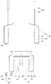
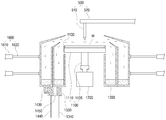
도 3은 본 발명의 실시예에 따른 제2 회수부가 제1 회수부에 착탈되는 것을 나타낸 도면이다.
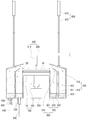
도 4 내지 도 7은 본 발명의 실시예에 따른 기판 처리 장치에 의하여 기판에 처리액이 도포되는 것을 나타낸 도면이다.
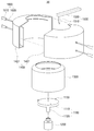
도 8은 본 발명의 다른 실시예에 따른 기판 처리 장치를 나타낸 도면이다.
도 9는 본 발명의 다른 실시예에 따른 제2 회수부가 제1 회수부에 착탈되는 것을 나타낸 도면이다.
도 10 내지 도 12는 본 발명의 다른 실시예에 따른 기판 처리 장치에 의하여 기판에 처리액이 도포되는 것을 나타낸 도면이다.
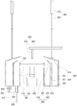
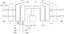
110, 1110: 척 플레이트 120, 1120: 회전축
200, 1200: 구동부 300, 1300: 제1 회수부
310: 제1 회수막 320: 제1 수용함
321: 제1 내측판 322: 제1 외측판
323: 제1 하측판 330, 1330: 제1 배출구
340, 1340: 제1 배출라인 400, 1400: 제2 회수부
410: 제2 회수막 420: 제2 수용함
421: 제2 내측판 422: 제2 외측판
423: 제2 하측판 430, 1430: 제2 배출구
440, 1440: 제2 배출라인 450, 1450: 배출관
500, 1500: 분사부 510, 1510: 분사 노즐
520, 1520: 이송부 600, 1600: 이동부
610, 1610: 실린더 620, 1620: 피스톤
1401, 1402: 부분 회수부
Claims (11)
- 기판을 지지하고, 회전하여 상기 기판에 분사된 처리액이 상기 기판에 도포되도록 하는 척;
상기 척의 측면을 감싸도록 환형으로 제공되고, 제1 회수막을 구비하여 상기 기판에서 이탈한 처리액을 회수하는 제1 회수부; 및
상기 제1 회수부의 측면을 감싸도록 환형으로 제공되고, 상기 제1 회수막보다 높은 위치에 배치된 제2 회수막을 구비하여 상기 기판에서 이탈한 처리액을 회수하는 제2 회수부를 포함하는 기판 처리 장치. - 제1 항에 있어서,
상기 처리액은 감광액을 포함하는 기판 처리 장치. - 제1 항에 있어서,
상기 제1 회수막 및 상기 제2 회수막은,
상기 기판의 측면을 감싸도록 환형으로 제공되고,
상기 기판의 중심으로 진행할수록 상향 경사지어 형성되는 기판 처리 장치. - 제3 항에 있어서,
상기 제1 회수막의 상부 말단은 제1 개구를 포함하고,
상기 제1 개구의 직경은 상기 기판의 직경보다 크게 형성되는 기판 처리 장치. - 제3 항에 있어서,
상기 제2 회수막의 상부 말단은 제2 개구를 포함하고,
상기 제2 개구의 직경은 상기 기판의 직경보다 작게 형성되는 기판 처리 장치. - 제1 항에 있어서,
상기 제2 회수부는 상기 제1 회수부에 착탈 가능한 기판 처리 장치. - 제6 항에 있어서,
상기 제2 회수부는,
상기 제1 회수부의 상측에서 하강하여 상기 제1 회수부에 부착되고,
상기 제1 회수부의 상측으로 상승하여 상기 제1 회수부에서 이탈되는 기판 처리 장치. - 제6 항에 있어서,
상기 제2 회수부는 서로 결합 및 결합 해제 가능한 복수의 부분 회수부를 포함하고,
상기 복수의 부분 회수부가 결합됨에 따라 상기 제2 회수부는 상기 제1 회수부에 부착되고,
상기 복수의 부분 회수부가 결합 해제됨에 따라 상기 제2 회수부는 상기 제1 회수부에서 이탈되는 기판 처리 장치. - 제8 항에 있어서,
상기 복수의 부분 회수부는 상기 기판의 회전 중심축에 수직한 방향으로 이동하여 상기 제1 회수부에 부착되거나 상기 제1 회수부에서 이탈되는 기판 처리 장치. - 제1 항에 있어서,
상기 제2 회수부는,
상기 기판에서 이탈한 처리액을 수용하는 제2 수용함; 및
상기 제2 수용함에 연결되어 상기 수용된 처리액을 배출하는 제2 배출구를 포함하는 기판 처리 장치. - 제10 항에 있어서,
상기 제2 배출구에 연결 및 연결 해제 가능하고, 상기 제2 배출구에서 배출된 처리액을 배출시키는 배출관을 더 포함하는 기판 처리 장치.
Priority Applications (1)
| Application Number | Priority Date | Filing Date | Title |
|---|---|---|---|
| KR1020180149700A KR102174762B1 (ko) | 2018-11-28 | 2018-11-28 | 기판 처리 장치 |
Applications Claiming Priority (1)
| Application Number | Priority Date | Filing Date | Title |
|---|---|---|---|
| KR1020180149700A KR102174762B1 (ko) | 2018-11-28 | 2018-11-28 | 기판 처리 장치 |
Publications (2)
| Publication Number | Publication Date |
|---|---|
| KR20200063680A true KR20200063680A (ko) | 2020-06-05 |
| KR102174762B1 KR102174762B1 (ko) | 2020-11-05 |
Family
ID=71089094
Family Applications (1)
| Application Number | Title | Priority Date | Filing Date |
|---|---|---|---|
| KR1020180149700A Active KR102174762B1 (ko) | 2018-11-28 | 2018-11-28 | 기판 처리 장치 |
Country Status (1)
| Country | Link |
|---|---|
| KR (1) | KR102174762B1 (ko) |
Citations (6)
| Publication number | Priority date | Publication date | Assignee | Title |
|---|---|---|---|---|
| JPH05190442A (ja) * | 1992-01-10 | 1993-07-30 | Hitachi Ltd | 薬液処理装置 |
| JPH104079A (ja) * | 1996-06-18 | 1998-01-06 | Dainippon Screen Mfg Co Ltd | 基板処理装置 |
| JPH11309404A (ja) * | 1998-04-30 | 1999-11-09 | Toshiba Corp | 基板処理装置 |
| JP2001267278A (ja) * | 2000-03-16 | 2001-09-28 | Mimasu Semiconductor Industry Co Ltd | 廃液回収機構付ウェーハ表面処理装置 |
| JP2001269609A (ja) * | 2000-03-28 | 2001-10-02 | Tokyo Electron Ltd | 塗布処理装置 |
| KR100488753B1 (ko) * | 2001-07-23 | 2005-05-11 | 다이닛뽕스크린 세이조오 가부시키가이샤 | 기판처리방법 및 그 장치 |
-
2018
- 2018-11-28 KR KR1020180149700A patent/KR102174762B1/ko active Active
Patent Citations (6)
| Publication number | Priority date | Publication date | Assignee | Title |
|---|---|---|---|---|
| JPH05190442A (ja) * | 1992-01-10 | 1993-07-30 | Hitachi Ltd | 薬液処理装置 |
| JPH104079A (ja) * | 1996-06-18 | 1998-01-06 | Dainippon Screen Mfg Co Ltd | 基板処理装置 |
| JPH11309404A (ja) * | 1998-04-30 | 1999-11-09 | Toshiba Corp | 基板処理装置 |
| JP2001267278A (ja) * | 2000-03-16 | 2001-09-28 | Mimasu Semiconductor Industry Co Ltd | 廃液回収機構付ウェーハ表面処理装置 |
| JP2001269609A (ja) * | 2000-03-28 | 2001-10-02 | Tokyo Electron Ltd | 塗布処理装置 |
| KR100488753B1 (ko) * | 2001-07-23 | 2005-05-11 | 다이닛뽕스크린 세이조오 가부시키가이샤 | 기판처리방법 및 그 장치 |
Also Published As
| Publication number | Publication date |
|---|---|
| KR102174762B1 (ko) | 2020-11-05 |
Similar Documents
| Publication | Publication Date | Title |
|---|---|---|
| KR101972294B1 (ko) | 기판 처리 장치 및 기판 처리 방법 | |
| KR101983897B1 (ko) | 기판 처리 장치 | |
| CN100342487C (zh) | 处理微电子工件的微环境反应器 | |
| KR101831545B1 (ko) | 기판 처리 장치 및 기판 처리 방법 | |
| JP4936146B2 (ja) | 基板処理装置及びこれを用いた基板処理装置洗浄方法 | |
| KR20140118850A (ko) | 기판 처리 장치 및 기판 처리 방법 | |
| KR101867748B1 (ko) | 기판 처리 장치 | |
| KR20160037775A (ko) | 기판 처리 장치 및 기판 처리 방법 | |
| KR101579509B1 (ko) | 기판 처리 장치 및 기판 처리 방법 | |
| US20190217344A1 (en) | Cup wash disk with shims | |
| TW200836841A (en) | Substrate processing apparatus and substrate processing method | |
| KR101770535B1 (ko) | 기판 처리 장치 | |
| KR20180034229A (ko) | 기판 처리 방법 및 기판 처리 장치 | |
| KR20200063680A (ko) | 기판 처리 장치 | |
| KR102284908B1 (ko) | 프리 디스펜스 유닛 및 기판 처리 장치 | |
| KR102203706B1 (ko) | 기판 처리 장치 및 기판 처리 방법 | |
| JP6799409B2 (ja) | 基板処理装置 | |
| JP3289208B2 (ja) | 洗浄処理方法及び洗浄処理装置 | |
| JP6280789B2 (ja) | 基板処理装置および基板処理方法 | |
| KR102792380B1 (ko) | 기판 처리 장치 | |
| JP2893151B2 (ja) | 処理装置及びその洗浄方法 | |
| KR20080088822A (ko) | 기판 처리 장치 | |
| KR20200055458A (ko) | 기판의 매엽식 세정장치 | |
| KR102139604B1 (ko) | 기판 처리 장치 및 기판 처리 방법 | |
| KR20220078990A (ko) | 기판 처리 장치 및 기판 처리 방법 |
Legal Events
| Date | Code | Title | Description |
|---|---|---|---|
| PA0109 | Patent application |
St.27 status event code: A-0-1-A10-A12-nap-PA0109 |
|
| PA0201 | Request for examination |
St.27 status event code: A-1-2-D10-D11-exm-PA0201 |
|
| D13-X000 | Search requested |
St.27 status event code: A-1-2-D10-D13-srh-X000 |
|
| D14-X000 | Search report completed |
St.27 status event code: A-1-2-D10-D14-srh-X000 |
|
| E902 | Notification of reason for refusal | ||
| PE0902 | Notice of grounds for rejection |
St.27 status event code: A-1-2-D10-D21-exm-PE0902 |
|
| E13-X000 | Pre-grant limitation requested |
St.27 status event code: A-2-3-E10-E13-lim-X000 |
|
| P11-X000 | Amendment of application requested |
St.27 status event code: A-2-2-P10-P11-nap-X000 |
|
| P13-X000 | Application amended |
St.27 status event code: A-2-2-P10-P13-nap-X000 |
|
| PG1501 | Laying open of application |
St.27 status event code: A-1-1-Q10-Q12-nap-PG1501 |
|
| E701 | Decision to grant or registration of patent right | ||
| PE0701 | Decision of registration |
St.27 status event code: A-1-2-D10-D22-exm-PE0701 |
|
| GRNT | Written decision to grant | ||
| PR0701 | Registration of establishment |
St.27 status event code: A-2-4-F10-F11-exm-PR0701 |
|
| PR1002 | Payment of registration fee |
St.27 status event code: A-2-2-U10-U11-oth-PR1002 Fee payment year number: 1 |
|
| PG1601 | Publication of registration |
St.27 status event code: A-4-4-Q10-Q13-nap-PG1601 |
|
| PN2301 | Change of applicant |
St.27 status event code: A-5-5-R10-R13-asn-PN2301 St.27 status event code: A-5-5-R10-R11-asn-PN2301 |
|
| R18-X000 | Changes to party contact information recorded |
St.27 status event code: A-5-5-R10-R18-oth-X000 |
|
| PR1001 | Payment of annual fee |
St.27 status event code: A-4-4-U10-U11-oth-PR1001 Fee payment year number: 4 |
|
| PR1001 | Payment of annual fee |
St.27 status event code: A-4-4-U10-U11-oth-PR1001 Fee payment year number: 5 |
|
| PN2301 | Change of applicant |
St.27 status event code: A-5-5-R10-R13-asn-PN2301 St.27 status event code: A-5-5-R10-R11-asn-PN2301 |
|
| PR1001 | Payment of annual fee |
St.27 status event code: A-4-4-U10-U11-oth-PR1001 Fee payment year number: 6 |
|
| U11 | Full renewal or maintenance fee paid |
Free format text: ST27 STATUS EVENT CODE: A-4-4-U10-U11-OTH-PR1001 (AS PROVIDED BY THE NATIONAL OFFICE) Year of fee payment: 6 |
|
| P22-X000 | Classification modified |
St.27 status event code: A-4-4-P10-P22-nap-X000 |