KR20200065543A - 기판 처리 장치 - Google Patents
기판 처리 장치 Download PDFInfo
- Publication number
- KR20200065543A KR20200065543A KR1020180152105A KR20180152105A KR20200065543A KR 20200065543 A KR20200065543 A KR 20200065543A KR 1020180152105 A KR1020180152105 A KR 1020180152105A KR 20180152105 A KR20180152105 A KR 20180152105A KR 20200065543 A KR20200065543 A KR 20200065543A
- Authority
- KR
- South Korea
- Prior art keywords
- substrate
- air
- edge
- seating surface
- processing apparatus
- Prior art date
- Legal status (The legal status is an assumption and is not a legal conclusion. Google has not performed a legal analysis and makes no representation as to the accuracy of the status listed.)
- Granted
Links
Images








Classifications
-
- H—ELECTRICITY
- H10—SEMICONDUCTOR DEVICES; ELECTRIC SOLID-STATE DEVICES NOT OTHERWISE PROVIDED FOR
- H10P—GENERIC PROCESSES OR APPARATUS FOR THE MANUFACTURE OR TREATMENT OF DEVICES COVERED BY CLASS H10
- H10P72/00—Handling or holding of wafers, substrates or devices during manufacture or treatment thereof
- H10P72/70—Handling or holding of wafers, substrates or devices during manufacture or treatment thereof for supporting or gripping
- H10P72/76—Handling or holding of wafers, substrates or devices during manufacture or treatment thereof for supporting or gripping using mechanical means, e.g. clamps or pinches
- H10P72/7604—Handling or holding of wafers, substrates or devices during manufacture or treatment thereof for supporting or gripping using mechanical means, e.g. clamps or pinches the wafers being placed on a susceptor, stage or support
- H10P72/7606—Handling or holding of wafers, substrates or devices during manufacture or treatment thereof for supporting or gripping using mechanical means, e.g. clamps or pinches the wafers being placed on a susceptor, stage or support characterised by edge clamping, e.g. clamping ring
-
- B—PERFORMING OPERATIONS; TRANSPORTING
- B25—HAND TOOLS; PORTABLE POWER-DRIVEN TOOLS; MANIPULATORS
- B25B—TOOLS OR BENCH DEVICES NOT OTHERWISE PROVIDED FOR, FOR FASTENING, CONNECTING, DISENGAGING, OR HOLDING
- B25B11/00—Work holders not covered by any preceding group in the subclass, e.g. magnetic work holders, vacuum work holders
- B25B11/005—Vacuum work holders
-
- H01L21/68721—
-
- H01L21/67028—
-
- H01L21/67103—
-
- H01L21/67288—
-
- H01L21/683—
-
- H01L21/68742—
-
- H—ELECTRICITY
- H10—SEMICONDUCTOR DEVICES; ELECTRIC SOLID-STATE DEVICES NOT OTHERWISE PROVIDED FOR
- H10P—GENERIC PROCESSES OR APPARATUS FOR THE MANUFACTURE OR TREATMENT OF DEVICES COVERED BY CLASS H10
- H10P72/00—Handling or holding of wafers, substrates or devices during manufacture or treatment thereof
- H10P72/04—Apparatus for manufacture or treatment
-
- H—ELECTRICITY
- H10—SEMICONDUCTOR DEVICES; ELECTRIC SOLID-STATE DEVICES NOT OTHERWISE PROVIDED FOR
- H10P—GENERIC PROCESSES OR APPARATUS FOR THE MANUFACTURE OR TREATMENT OF DEVICES COVERED BY CLASS H10
- H10P72/00—Handling or holding of wafers, substrates or devices during manufacture or treatment thereof
- H10P72/04—Apparatus for manufacture or treatment
- H10P72/0402—Apparatus for fluid treatment
- H10P72/0406—Apparatus for fluid treatment for cleaning followed by drying, rinsing, stripping, blasting or the like
-
- H—ELECTRICITY
- H10—SEMICONDUCTOR DEVICES; ELECTRIC SOLID-STATE DEVICES NOT OTHERWISE PROVIDED FOR
- H10P—GENERIC PROCESSES OR APPARATUS FOR THE MANUFACTURE OR TREATMENT OF DEVICES COVERED BY CLASS H10
- H10P72/00—Handling or holding of wafers, substrates or devices during manufacture or treatment thereof
- H10P72/04—Apparatus for manufacture or treatment
- H10P72/0431—Apparatus for thermal treatment
- H10P72/0432—Apparatus for thermal treatment mainly by conduction
-
- H—ELECTRICITY
- H10—SEMICONDUCTOR DEVICES; ELECTRIC SOLID-STATE DEVICES NOT OTHERWISE PROVIDED FOR
- H10P—GENERIC PROCESSES OR APPARATUS FOR THE MANUFACTURE OR TREATMENT OF DEVICES COVERED BY CLASS H10
- H10P72/00—Handling or holding of wafers, substrates or devices during manufacture or treatment thereof
- H10P72/06—Apparatus for monitoring, sorting, marking, testing or measuring
- H10P72/0616—Monitoring of warpages, curvatures, damages, defects or the like
-
- H—ELECTRICITY
- H10—SEMICONDUCTOR DEVICES; ELECTRIC SOLID-STATE DEVICES NOT OTHERWISE PROVIDED FOR
- H10P—GENERIC PROCESSES OR APPARATUS FOR THE MANUFACTURE OR TREATMENT OF DEVICES COVERED BY CLASS H10
- H10P72/00—Handling or holding of wafers, substrates or devices during manufacture or treatment thereof
- H10P72/50—Handling or holding of wafers, substrates or devices during manufacture or treatment thereof for positioning, orientation or alignment
-
- H—ELECTRICITY
- H10—SEMICONDUCTOR DEVICES; ELECTRIC SOLID-STATE DEVICES NOT OTHERWISE PROVIDED FOR
- H10P—GENERIC PROCESSES OR APPARATUS FOR THE MANUFACTURE OR TREATMENT OF DEVICES COVERED BY CLASS H10
- H10P72/00—Handling or holding of wafers, substrates or devices during manufacture or treatment thereof
- H10P72/70—Handling or holding of wafers, substrates or devices during manufacture or treatment thereof for supporting or gripping
-
- H—ELECTRICITY
- H10—SEMICONDUCTOR DEVICES; ELECTRIC SOLID-STATE DEVICES NOT OTHERWISE PROVIDED FOR
- H10P—GENERIC PROCESSES OR APPARATUS FOR THE MANUFACTURE OR TREATMENT OF DEVICES COVERED BY CLASS H10
- H10P72/00—Handling or holding of wafers, substrates or devices during manufacture or treatment thereof
- H10P72/70—Handling or holding of wafers, substrates or devices during manufacture or treatment thereof for supporting or gripping
- H10P72/76—Handling or holding of wafers, substrates or devices during manufacture or treatment thereof for supporting or gripping using mechanical means, e.g. clamps or pinches
- H10P72/7604—Handling or holding of wafers, substrates or devices during manufacture or treatment thereof for supporting or gripping using mechanical means, e.g. clamps or pinches the wafers being placed on a susceptor, stage or support
- H10P72/7608—Handling or holding of wafers, substrates or devices during manufacture or treatment thereof for supporting or gripping using mechanical means, e.g. clamps or pinches the wafers being placed on a susceptor, stage or support characterised by a plurality of separate clamping members, e.g. clamping fingers
-
- H—ELECTRICITY
- H10—SEMICONDUCTOR DEVICES; ELECTRIC SOLID-STATE DEVICES NOT OTHERWISE PROVIDED FOR
- H10P—GENERIC PROCESSES OR APPARATUS FOR THE MANUFACTURE OR TREATMENT OF DEVICES COVERED BY CLASS H10
- H10P72/00—Handling or holding of wafers, substrates or devices during manufacture or treatment thereof
- H10P72/70—Handling or holding of wafers, substrates or devices during manufacture or treatment thereof for supporting or gripping
- H10P72/76—Handling or holding of wafers, substrates or devices during manufacture or treatment thereof for supporting or gripping using mechanical means, e.g. clamps or pinches
- H10P72/7604—Handling or holding of wafers, substrates or devices during manufacture or treatment thereof for supporting or gripping using mechanical means, e.g. clamps or pinches the wafers being placed on a susceptor, stage or support
- H10P72/7611—Handling or holding of wafers, substrates or devices during manufacture or treatment thereof for supporting or gripping using mechanical means, e.g. clamps or pinches the wafers being placed on a susceptor, stage or support characterised by edge profile or support profile
-
- H—ELECTRICITY
- H10—SEMICONDUCTOR DEVICES; ELECTRIC SOLID-STATE DEVICES NOT OTHERWISE PROVIDED FOR
- H10P—GENERIC PROCESSES OR APPARATUS FOR THE MANUFACTURE OR TREATMENT OF DEVICES COVERED BY CLASS H10
- H10P72/00—Handling or holding of wafers, substrates or devices during manufacture or treatment thereof
- H10P72/70—Handling or holding of wafers, substrates or devices during manufacture or treatment thereof for supporting or gripping
- H10P72/76—Handling or holding of wafers, substrates or devices during manufacture or treatment thereof for supporting or gripping using mechanical means, e.g. clamps or pinches
- H10P72/7604—Handling or holding of wafers, substrates or devices during manufacture or treatment thereof for supporting or gripping using mechanical means, e.g. clamps or pinches the wafers being placed on a susceptor, stage or support
- H10P72/7612—Handling or holding of wafers, substrates or devices during manufacture or treatment thereof for supporting or gripping using mechanical means, e.g. clamps or pinches the wafers being placed on a susceptor, stage or support characterised by lifting arrangements, e.g. lift pins
-
- H—ELECTRICITY
- H10—SEMICONDUCTOR DEVICES; ELECTRIC SOLID-STATE DEVICES NOT OTHERWISE PROVIDED FOR
- H10P—GENERIC PROCESSES OR APPARATUS FOR THE MANUFACTURE OR TREATMENT OF DEVICES COVERED BY CLASS H10
- H10P72/00—Handling or holding of wafers, substrates or devices during manufacture or treatment thereof
- H10P72/70—Handling or holding of wafers, substrates or devices during manufacture or treatment thereof for supporting or gripping
- H10P72/76—Handling or holding of wafers, substrates or devices during manufacture or treatment thereof for supporting or gripping using mechanical means, e.g. clamps or pinches
- H10P72/7604—Handling or holding of wafers, substrates or devices during manufacture or treatment thereof for supporting or gripping using mechanical means, e.g. clamps or pinches the wafers being placed on a susceptor, stage or support
- H10P72/7614—Handling or holding of wafers, substrates or devices during manufacture or treatment thereof for supporting or gripping using mechanical means, e.g. clamps or pinches the wafers being placed on a susceptor, stage or support characterised by a plurality of individual support members, e.g. support posts or protrusions
-
- H—ELECTRICITY
- H10—SEMICONDUCTOR DEVICES; ELECTRIC SOLID-STATE DEVICES NOT OTHERWISE PROVIDED FOR
- H10P—GENERIC PROCESSES OR APPARATUS FOR THE MANUFACTURE OR TREATMENT OF DEVICES COVERED BY CLASS H10
- H10P72/00—Handling or holding of wafers, substrates or devices during manufacture or treatment thereof
- H10P72/70—Handling or holding of wafers, substrates or devices during manufacture or treatment thereof for supporting or gripping
- H10P72/76—Handling or holding of wafers, substrates or devices during manufacture or treatment thereof for supporting or gripping using mechanical means, e.g. clamps or pinches
- H10P72/7604—Handling or holding of wafers, substrates or devices during manufacture or treatment thereof for supporting or gripping using mechanical means, e.g. clamps or pinches the wafers being placed on a susceptor, stage or support
- H10P72/7624—Handling or holding of wafers, substrates or devices during manufacture or treatment thereof for supporting or gripping using mechanical means, e.g. clamps or pinches the wafers being placed on a susceptor, stage or support characterised by the mechanical construction of the susceptor, stage or support
-
- H—ELECTRICITY
- H10—SEMICONDUCTOR DEVICES; ELECTRIC SOLID-STATE DEVICES NOT OTHERWISE PROVIDED FOR
- H10P—GENERIC PROCESSES OR APPARATUS FOR THE MANUFACTURE OR TREATMENT OF DEVICES COVERED BY CLASS H10
- H10P72/00—Handling or holding of wafers, substrates or devices during manufacture or treatment thereof
- H10P72/70—Handling or holding of wafers, substrates or devices during manufacture or treatment thereof for supporting or gripping
- H10P72/78—Handling or holding of wafers, substrates or devices during manufacture or treatment thereof for supporting or gripping using vacuum or suction, e.g. Bernoulli chucks
-
- H—ELECTRICITY
- H10—SEMICONDUCTOR DEVICES; ELECTRIC SOLID-STATE DEVICES NOT OTHERWISE PROVIDED FOR
- H10P—GENERIC PROCESSES OR APPARATUS FOR THE MANUFACTURE OR TREATMENT OF DEVICES COVERED BY CLASS H10
- H10P72/00—Handling or holding of wafers, substrates or devices during manufacture or treatment thereof
- H10P72/70—Handling or holding of wafers, substrates or devices during manufacture or treatment thereof for supporting or gripping
- H10P72/74—Handling or holding of wafers, substrates or devices during manufacture or treatment thereof for supporting or gripping using temporarily an auxiliary support
- H10P72/7408—Handling or holding of wafers, substrates or devices during manufacture or treatment thereof for supporting or gripping using temporarily an auxiliary support the auxiliary support including alignment aids
Landscapes
- Engineering & Computer Science (AREA)
- Mechanical Engineering (AREA)
- Container, Conveyance, Adherence, Positioning, Of Wafer (AREA)
Abstract
Description
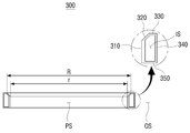
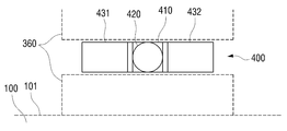
도 3은 본 발명의 실시예예 따른 가이드 링의 단면도이다.
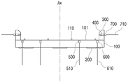
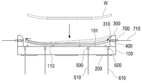
도 4는 본 발명의 실시예에 따른 기판 처리 장치에 기판이 안착된 것을 나타낸 도면이다.
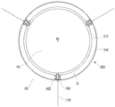
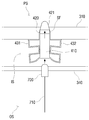
도 5는 본 발명의 실시예에 따른 가이드 링에 센터링부가 설치된 것을 나타낸 도면이다.
도 6은 본 발명의 실시예에 따른 센터링부가 설치되는 가이드 링의 일부분을 나타낸 도면이다.
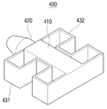
도 7 및 도 8은 본 발명의 실시예예 따른 센터링부를 나타낸 도면이다.
도 9는 본 발명의 실시예에 따른 센터링부의 배치 자세를 나타낸 도면이다.
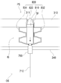
도 10은 본 발명의 실시예에 따른 센터링부의 움직임을 나타낸 도면이다.
도 11 및 도 12는 본 발명의 실시예에 따른 센터링부의 센터링 동작을 나타낸 도면이다.
도 13 및 도 14는 본 발명의 실시예에 따른 기판 처리 장치에 안착된 기판이 센터링되는 것을 나타낸 도면이다.
도 15 및 도 16은 본 발명의 다른 실시예에 따른 센터링부의 센터링 동작을 나타낸 도면이다.
101: 안착면 110: 지지핀
200: 가열부 300: 가이드 링
310: 내측판 320: 경사판
330: 상측판 340: 외측판
350: 하측판 400, 800: 센터링부
410, 810: 몸체 420, 820: 헤드
431, 432, 831, 832: 탄성체 500, 600: 에어 흡입 노즐
510, 610: 에어 흡입 라인 700: 에어 노즐
710: 에어 라인
Claims (14)
- 안착면을 구비하여 기판을 지지하는 기판 지지부;
상기 기판을 감싸도록 상기 기판 지지부의 가장자리를 따라 환형으로 배치된 가이드 링; 및
상기 가이드 링의 내부에 구비되고, 상기 안착면에 평행한 방향으로 이동하여 상기 기판의 가장자리를 가압함으로써 상기 기판을 센터링하는 센터링부를 포함하는 기판 처리 장치. - 제1 항에 있어서,
상기 기판 지지부는 에어를 흡입하는 제1 및 제2 에어 흡입 노즐을 포함하되,
상기 제1 에어 흡입 노즐은 흡입력으로 상기 기판을 상기 기판 지지부에 고정시키고,
상기 제2 에어 흡입 노즐은 흡입력으로 상기 기판과 상기 기판 지지부의 사이에 존재하는 파티클을 흡입하는 기판 처리 장치. - 제2 항에 있어서,
상기 제1 에어 흡입 노즐은 상기 안착면의 중심에 인접하여 배치되고,
상기 제2 에어 흡입 노즐은 상기 안착면의 가장자리를 따라 배치되는 기판 처리 장치. - 제1 항에 있어서,
상기 가이드 링은,
상기 안착면에 수직한 넓은 면을 갖고, 상기 기판을 감싸도록 환형으로 형성된 내측판; 및
상기 내측판의 상측 말단에서 상기 기판을 감싸도록 환형으로 연장 형성되고, 상기 안착면에서 멀어질수록 직경이 증가하는 경사판을 포함하는 기판 처리 장치. - 제4 항에 있어서,
상기 안착면에 대한 상기 내측판의 높이는 상기 기판 지지부에 지지된 기판의 가장자리의 높이에 비하여 높게 형성되는 기판 처리 장치. - 제5 항에 있어서,
상기 기판 지지부는 상기 기판을 지지하는 지지 핀을 포함하고,
상기 기판은 중심부와 상기 안착면간의 거리에 비하여 그 가장자리와 상기 안착면간의 거리가 크게 형성되는 워피지(warpage) 기판을 포함하며,
상기 안착면에 대한 상기 내측판의 높이는 상기 지지 핀에 지지된 상기 워피지 기판의 가장자리의 높이에 비하여 높게 형성되는 기판 처리 장치. - 제1 항에 있어서,
상기 기판 처리 장치는 상기 기판 지지부에 부착되어 상기 기판을 가열하는 가열부를 더 포함하는 기판 처리 장치. - 제1 항에 있어서,
상기 센터링부는,
일측으로 길게 형성된 몸체;
상기 몸체의 일측 말단에 구비되고, 상기 몸체와 함께 이동하여 상기 기판의 가장자리를 가압하는 헤드; 및
일측이 상기 기판 지지부에 고정되고, 타측이 상기 몸체에 연결되어 상기 기판 지지부에 대한 상기 몸체의 탄성 이동을 위한 탄성력을 제공하는 탄성체를 포함하는 기판 처리 장치. - 제8 항에 있어서,
상기 탄성체는,
상기 몸체의 일측에 배치된 제1 탄성체; 및
상기 몸체를 중심으로 상기 제1 탄성체가 배치된 상기 일측의 반대측에 배치된 제2 탄성체를 포함하는 기판 처리 장치. - 제9 항에 있어서,
상기 몸체, 상기 제1 탄성체 및 상기 제2 탄성체의 결합체는 판의 형상을 갖고,
상기 결합체는 그 넓은 면이 상기 안착면에 평행하게 배치되는 기판 처리 장치. - 제8 항에 있어서,
상기 헤드는 상기 기판을 향할수록 직경이 작아지는 경사부를 포함하는 기판 처리 장치. - 제11 항에 있어서,
상기 가이드 링은 상기 경사부의 형상에 대응하는 경사면을 구비한 관통홀을 구비하고,
상기 경사부가 상기 경사면에 접하는 경우 상기 헤드의 일부가 상기 관통홀의 외부로 노출되어 상기 기판의 가장자리를 가압하는 기판 처리 장치. - 제12 항에 있어서,
상기 기판 지지부는 에어를 분사하는 에어 노즐을 포함하고,
상기 에어 노즐에서 분사된 에어가 상기 몸체를 밀어냄에 따라 상기 헤드가 이동하여 상기 기판의 가장자리를 가압하고,
상기 에어 노즐의 에어 분사가 중단되는 경우 상기 탄성체의 탄성력에 의해 상기 몸체가 원위치로 복귀하여 상기 헤드에 의한 상기 기판의 가장자리 가압이 해제되는 기판 처리 장치. - 제12 항에 있어서,
상기 기판 지지부는 에어를 흡입하는 에어 노즐을 포함하고,
상기 에어 노즐의 에어 흡입이 중단된 경우 상기 탄성체의 탄성력에 의해 상기 몸체에 연결된 상기 헤드가 상기 기판의 가장자리를 가압하고,
상기 에어 노즐이 에어를 흡입하여 상기 몸체를 당기는 경우 상기 헤드가 이동하여 상기 헤드에 의한 상기 기판의 가장자리 가압이 해제되는 기판 처리 장치.
Priority Applications (3)
| Application Number | Priority Date | Filing Date | Title |
|---|---|---|---|
| KR1020180152105A KR102195920B1 (ko) | 2018-11-30 | 2018-11-30 | 기판 처리 장치 |
| CN201911145592.5A CN111261570B (zh) | 2018-11-30 | 2019-11-21 | 基板处理装置 |
| US16/693,569 US11766765B2 (en) | 2018-11-30 | 2019-11-25 | Substrate treatment apparatus |
Applications Claiming Priority (1)
| Application Number | Priority Date | Filing Date | Title |
|---|---|---|---|
| KR1020180152105A KR102195920B1 (ko) | 2018-11-30 | 2018-11-30 | 기판 처리 장치 |
Publications (2)
| Publication Number | Publication Date |
|---|---|
| KR20200065543A true KR20200065543A (ko) | 2020-06-09 |
| KR102195920B1 KR102195920B1 (ko) | 2020-12-29 |
Family
ID=70848606
Family Applications (1)
| Application Number | Title | Priority Date | Filing Date |
|---|---|---|---|
| KR1020180152105A Active KR102195920B1 (ko) | 2018-11-30 | 2018-11-30 | 기판 처리 장치 |
Country Status (3)
| Country | Link |
|---|---|
| US (1) | US11766765B2 (ko) |
| KR (1) | KR102195920B1 (ko) |
| CN (1) | CN111261570B (ko) |
Families Citing this family (1)
| Publication number | Priority date | Publication date | Assignee | Title |
|---|---|---|---|---|
| US11217474B2 (en) * | 2019-12-06 | 2022-01-04 | Government Of The United States Of America, As Represented By The Secretary Of Commerce | Non-vacuum, non-contact spinner wafer chuck |
Citations (4)
| Publication number | Priority date | Publication date | Assignee | Title |
|---|---|---|---|---|
| JPH0837227A (ja) * | 1994-07-25 | 1996-02-06 | Hitachi Ltd | ウエハチャックおよびそれを用いた露光装置 |
| JP2003158173A (ja) * | 2001-11-20 | 2003-05-30 | Oki Electric Ind Co Ltd | ウェハホルダ |
| KR20040073173A (ko) * | 2003-02-13 | 2004-08-19 | 삼성전자주식회사 | 반도체 소자 제조 장치 및 반도체 기판을 상기 장치 내의서포터 상에 안착시키는 방법 |
| KR20090075367A (ko) * | 2008-01-04 | 2009-07-08 | 삼성전자주식회사 | 기판 지지대, 이를 포함하는 기판 처리 장치 및 기판 정렬방법 |
Family Cites Families (17)
| Publication number | Priority date | Publication date | Assignee | Title |
|---|---|---|---|---|
| KR100601988B1 (ko) * | 2005-02-05 | 2006-07-18 | 삼성전자주식회사 | 웨이퍼 가열 장비 |
| US7395933B2 (en) * | 2005-06-14 | 2008-07-08 | Intel Corporation | Carrier to hold semiconductor device using opposed rollers |
| WO2007013605A1 (ja) * | 2005-07-28 | 2007-02-01 | Tokyo Electron Limited | 基板処理方法および基板処理装置 |
| JP4781901B2 (ja) * | 2006-05-08 | 2011-09-28 | 東京エレクトロン株式会社 | 熱処理方法,プログラム及び熱処理装置 |
| KR20090048202A (ko) * | 2007-11-09 | 2009-05-13 | 주식회사 에이디피엔지니어링 | 기판 안착 장치 및 기판 안착 방법 |
| KR20100034450A (ko) * | 2008-09-24 | 2010-04-01 | 삼성전자주식회사 | 기판접합장치 |
| KR20100129566A (ko) * | 2009-06-01 | 2010-12-09 | 주식회사 유진테크 | 기판지지유닛 및 이를 포함하는 기판처리장치 |
| JP5902085B2 (ja) | 2009-08-07 | 2016-04-13 | アプライド マテリアルズ インコーポレイテッドApplied Materials,Incorporated | 処理チャンバ内で基板を位置決めするための装置及び処理チャンバ内で基板をセンタリングするための方法 |
| JP5861598B2 (ja) * | 2012-08-31 | 2016-02-16 | 株式会社デンソー | 半導体ウエハの表面処理装置および表面処理方法 |
| DE102012111167A1 (de) * | 2012-11-20 | 2014-05-22 | Aixtron Se | Vorrichtung zum Ausrichten eines Wafers auf einem Waferträger |
| KR102091291B1 (ko) * | 2013-02-14 | 2020-03-19 | 가부시키가이샤 스크린 홀딩스 | 기판 처리 장치 및 기판 처리 방법 |
| TWI636518B (zh) * | 2013-04-23 | 2018-09-21 | 荏原製作所股份有限公司 | 基板處理裝置及處理基板之製造方法 |
| JP6232297B2 (ja) * | 2014-01-21 | 2017-11-15 | 株式会社荏原製作所 | 基板保持装置および研磨装置 |
| KR101957832B1 (ko) * | 2014-11-14 | 2019-03-14 | 주식회사 원익아이피에스 | 기판처리장치 |
| KR102000021B1 (ko) * | 2016-11-30 | 2019-07-17 | 세메스 주식회사 | 기판 지지 유닛, 열처리 유닛 및 이를 포함하는 기판 처리 장치 |
| KR102538847B1 (ko) | 2016-12-15 | 2023-05-31 | 세메스 주식회사 | 진공척 |
| WO2021194782A1 (en) * | 2020-03-27 | 2021-09-30 | Corning Incorporated | Positioning devices for radially positioning substrates with respect to an air bearing device |
-
2018
- 2018-11-30 KR KR1020180152105A patent/KR102195920B1/ko active Active
-
2019
- 2019-11-21 CN CN201911145592.5A patent/CN111261570B/zh active Active
- 2019-11-25 US US16/693,569 patent/US11766765B2/en active Active
Patent Citations (4)
| Publication number | Priority date | Publication date | Assignee | Title |
|---|---|---|---|---|
| JPH0837227A (ja) * | 1994-07-25 | 1996-02-06 | Hitachi Ltd | ウエハチャックおよびそれを用いた露光装置 |
| JP2003158173A (ja) * | 2001-11-20 | 2003-05-30 | Oki Electric Ind Co Ltd | ウェハホルダ |
| KR20040073173A (ko) * | 2003-02-13 | 2004-08-19 | 삼성전자주식회사 | 반도체 소자 제조 장치 및 반도체 기판을 상기 장치 내의서포터 상에 안착시키는 방법 |
| KR20090075367A (ko) * | 2008-01-04 | 2009-07-08 | 삼성전자주식회사 | 기판 지지대, 이를 포함하는 기판 처리 장치 및 기판 정렬방법 |
Also Published As
| Publication number | Publication date |
|---|---|
| KR102195920B1 (ko) | 2020-12-29 |
| CN111261570A (zh) | 2020-06-09 |
| US20200171626A1 (en) | 2020-06-04 |
| CN111261570B (zh) | 2023-07-14 |
| US11766765B2 (en) | 2023-09-26 |
Similar Documents
| Publication | Publication Date | Title |
|---|---|---|
| JP6349343B2 (ja) | 吸着ユニット、板状部材搬送ユニット、樹脂封止装置、板状部材搬送方法および樹脂封止方法 | |
| CN102576689B (zh) | 基板处理系统、基板支架、基板支架对、基板接合装置及器件的制造方法 | |
| US8336866B2 (en) | Stage for substrate | |
| US7326300B2 (en) | Coating apparatus and method using the same | |
| JP5508709B2 (ja) | 塗布処理装置および基板処理装置 | |
| JP2022074028A (ja) | 搬送ハンド及び基板処理装置 | |
| TW201507058A (zh) | 基板之保持裝置及緊貼曝光裝置以及近接曝光裝置 | |
| KR20200065543A (ko) | 기판 처리 장치 | |
| JP5745964B2 (ja) | 半導体装置の製造方法及び半導体製造装置 | |
| JP2001189260A (ja) | 液処理装置及びその方法 | |
| JP6612670B2 (ja) | 基板処理装置、及び、基板処理方法 | |
| KR20030028985A (ko) | 반도체 소자 제조용 장비에서의 웨이퍼 척 | |
| JPH05299492A (ja) | ウエハの位置決め装置 | |
| JP2011249519A (ja) | 半導体装置の製造方法 | |
| KR20100077584A (ko) | 반도체 제조설비 | |
| KR20100108185A (ko) | 기판 열처리 장치 | |
| JP2000232058A (ja) | 現像方法及びノズル装置 | |
| JP3563211B2 (ja) | レジスト塗布装置 | |
| US20240194517A1 (en) | Substrate processing apparatus | |
| JP2013135137A (ja) | 板状物の保持方法及び板状物の加工方法 | |
| KR20210036129A (ko) | 베이크 장치 | |
| KR20100007774A (ko) | 비접촉 웨이퍼 이송 장치 | |
| JPH04233296A (ja) | 半導体装置の実装方法 | |
| JP5925940B2 (ja) | 半導体装置の製造方法及び半導体製造装置 | |
| JPH04163909A (ja) | 半導体装置の製造方法 |
Legal Events
| Date | Code | Title | Description |
|---|---|---|---|
| PA0109 | Patent application |
St.27 status event code: A-0-1-A10-A12-nap-PA0109 |
|
| PA0201 | Request for examination |
St.27 status event code: A-1-2-D10-D11-exm-PA0201 |
|
| D13-X000 | Search requested |
St.27 status event code: A-1-2-D10-D13-srh-X000 |
|
| D14-X000 | Search report completed |
St.27 status event code: A-1-2-D10-D14-srh-X000 |
|
| E902 | Notification of reason for refusal | ||
| PE0902 | Notice of grounds for rejection |
St.27 status event code: A-1-2-D10-D21-exm-PE0902 |
|
| PG1501 | Laying open of application |
St.27 status event code: A-1-1-Q10-Q12-nap-PG1501 |
|
| E13-X000 | Pre-grant limitation requested |
St.27 status event code: A-2-3-E10-E13-lim-X000 |
|
| P11-X000 | Amendment of application requested |
St.27 status event code: A-2-2-P10-P11-nap-X000 |
|
| P13-X000 | Application amended |
St.27 status event code: A-2-2-P10-P13-nap-X000 |
|
| E701 | Decision to grant or registration of patent right | ||
| PE0701 | Decision of registration |
St.27 status event code: A-1-2-D10-D22-exm-PE0701 |
|
| GRNT | Written decision to grant | ||
| PR0701 | Registration of establishment |
St.27 status event code: A-2-4-F10-F11-exm-PR0701 |
|
| PR1002 | Payment of registration fee |
St.27 status event code: A-2-2-U10-U11-oth-PR1002 Fee payment year number: 1 |
|
| PG1601 | Publication of registration |
St.27 status event code: A-4-4-Q10-Q13-nap-PG1601 |
|
| PN2301 | Change of applicant |
St.27 status event code: A-5-5-R10-R13-asn-PN2301 St.27 status event code: A-5-5-R10-R11-asn-PN2301 |
|
| R18-X000 | Changes to party contact information recorded |
St.27 status event code: A-5-5-R10-R18-oth-X000 |
|
| PR1001 | Payment of annual fee |
St.27 status event code: A-4-4-U10-U11-oth-PR1001 Fee payment year number: 4 |
|
| PR1001 | Payment of annual fee |
St.27 status event code: A-4-4-U10-U11-oth-PR1001 Fee payment year number: 5 |
|
| PN2301 | Change of applicant |
St.27 status event code: A-5-5-R10-R13-asn-PN2301 St.27 status event code: A-5-5-R10-R11-asn-PN2301 |
|
| PR1001 | Payment of annual fee |
St.27 status event code: A-4-4-U10-U11-oth-PR1001 Fee payment year number: 6 |
|
| U11 | Full renewal or maintenance fee paid |
Free format text: ST27 STATUS EVENT CODE: A-4-4-U10-U11-OTH-PR1001 (AS PROVIDED BY THE NATIONAL OFFICE) Year of fee payment: 6 |
|
| P22-X000 | Classification modified |
St.27 status event code: A-4-4-P10-P22-nap-X000 |