KR20200066920A - 디스플레이 장치 - Google Patents
디스플레이 장치 Download PDFInfo
- Publication number
- KR20200066920A KR20200066920A KR1020180153656A KR20180153656A KR20200066920A KR 20200066920 A KR20200066920 A KR 20200066920A KR 1020180153656 A KR1020180153656 A KR 1020180153656A KR 20180153656 A KR20180153656 A KR 20180153656A KR 20200066920 A KR20200066920 A KR 20200066920A
- Authority
- KR
- South Korea
- Prior art keywords
- circuit board
- display device
- guide
- elastic member
- panel
- Prior art date
- Legal status (The legal status is an assumption and is not a legal conclusion. Google has not performed a legal analysis and makes no representation as to the accuracy of the status listed.)
- Granted
Links
Images



Classifications
-
- H—ELECTRICITY
- H05—ELECTRIC TECHNIQUES NOT OTHERWISE PROVIDED FOR
- H05K—PRINTED CIRCUITS; CASINGS OR CONSTRUCTIONAL DETAILS OF ELECTRIC APPARATUS; MANUFACTURE OF ASSEMBLAGES OF ELECTRICAL COMPONENTS
- H05K7/00—Constructional details common to different types of electric apparatus
- H05K7/14—Mounting supporting structure in casing or on frame or rack
- H05K7/1401—Mounting supporting structure in casing or on frame or rack comprising clamping or extracting means
- H05K7/1402—Mounting supporting structure in casing or on frame or rack comprising clamping or extracting means for securing or extracting printed circuit boards
- H05K7/1405—Mounting supporting structure in casing or on frame or rack comprising clamping or extracting means for securing or extracting printed circuit boards by clips or resilient members, e.g. hooks
-
- H—ELECTRICITY
- H05—ELECTRIC TECHNIQUES NOT OTHERWISE PROVIDED FOR
- H05K—PRINTED CIRCUITS; CASINGS OR CONSTRUCTIONAL DETAILS OF ELECTRIC APPARATUS; MANUFACTURE OF ASSEMBLAGES OF ELECTRICAL COMPONENTS
- H05K7/00—Constructional details common to different types of electric apparatus
- H05K7/20—Modifications to facilitate cooling, ventilating, or heating
- H05K7/20954—Modifications to facilitate cooling, ventilating, or heating for display panels
- H05K7/20963—Heat transfer by conduction from internal heat source to heat radiating structure
-
- G—PHYSICS
- G06—COMPUTING OR CALCULATING; COUNTING
- G06F—ELECTRIC DIGITAL DATA PROCESSING
- G06F3/00—Input arrangements for transferring data to be processed into a form capable of being handled by the computer; Output arrangements for transferring data from processing unit to output unit, e.g. interface arrangements
- G06F3/01—Input arrangements or combined input and output arrangements for interaction between user and computer
- G06F3/03—Arrangements for converting the position or the displacement of a member into a coded form
- G06F3/041—Digitisers, e.g. for touch screens or touch pads, characterised by the transducing means
-
- G—PHYSICS
- G09—EDUCATION; CRYPTOGRAPHY; DISPLAY; ADVERTISING; SEALS
- G09G—ARRANGEMENTS OR CIRCUITS FOR CONTROL OF INDICATING DEVICES USING STATIC MEANS TO PRESENT VARIABLE INFORMATION
- G09G3/00—Control arrangements or circuits, of interest only in connection with visual indicators other than cathode-ray tubes
- G09G3/20—Control arrangements or circuits, of interest only in connection with visual indicators other than cathode-ray tubes for presentation of an assembly of a number of characters, e.g. a page, by composing the assembly by combination of individual elements arranged in a matrix no fixed position being assigned to or needed to be assigned to the individual characters or partial characters
- G09G3/2007—Display of intermediate tones
- G09G3/2074—Display of intermediate tones using sub-pixels
-
- H—ELECTRICITY
- H05—ELECTRIC TECHNIQUES NOT OTHERWISE PROVIDED FOR
- H05K—PRINTED CIRCUITS; CASINGS OR CONSTRUCTIONAL DETAILS OF ELECTRIC APPARATUS; MANUFACTURE OF ASSEMBLAGES OF ELECTRICAL COMPONENTS
- H05K1/00—Printed circuits
- H05K1/02—Details
- H05K1/0284—Details of three-dimensional rigid printed circuit boards
-
- H—ELECTRICITY
- H05—ELECTRIC TECHNIQUES NOT OTHERWISE PROVIDED FOR
- H05K—PRINTED CIRCUITS; CASINGS OR CONSTRUCTIONAL DETAILS OF ELECTRIC APPARATUS; MANUFACTURE OF ASSEMBLAGES OF ELECTRICAL COMPONENTS
- H05K5/00—Casings, cabinets or drawers for electric apparatus
- H05K5/0017—Casings, cabinets or drawers for electric apparatus with operator interface units
-
- H—ELECTRICITY
- H05—ELECTRIC TECHNIQUES NOT OTHERWISE PROVIDED FOR
- H05K—PRINTED CIRCUITS; CASINGS OR CONSTRUCTIONAL DETAILS OF ELECTRIC APPARATUS; MANUFACTURE OF ASSEMBLAGES OF ELECTRICAL COMPONENTS
- H05K5/00—Casings, cabinets or drawers for electric apparatus
- H05K5/0017—Casings, cabinets or drawers for electric apparatus with operator interface units
- H05K5/0018—Casings, cabinets or drawers for electric apparatus with operator interface units having an electronic display
-
- H—ELECTRICITY
- H05—ELECTRIC TECHNIQUES NOT OTHERWISE PROVIDED FOR
- H05K—PRINTED CIRCUITS; CASINGS OR CONSTRUCTIONAL DETAILS OF ELECTRIC APPARATUS; MANUFACTURE OF ASSEMBLAGES OF ELECTRICAL COMPONENTS
- H05K5/00—Casings, cabinets or drawers for electric apparatus
- H05K5/06—Hermetically-sealed casings
-
- H—ELECTRICITY
- H05—ELECTRIC TECHNIQUES NOT OTHERWISE PROVIDED FOR
- H05K—PRINTED CIRCUITS; CASINGS OR CONSTRUCTIONAL DETAILS OF ELECTRIC APPARATUS; MANUFACTURE OF ASSEMBLAGES OF ELECTRICAL COMPONENTS
- H05K1/00—Printed circuits
- H05K1/02—Details
- H05K1/14—Structural association of two or more printed circuits
- H05K1/147—Structural association of two or more printed circuits at least one of the printed circuits being bent or folded, e.g. by using a flexible printed circuit
-
- H—ELECTRICITY
- H05—ELECTRIC TECHNIQUES NOT OTHERWISE PROVIDED FOR
- H05K—PRINTED CIRCUITS; CASINGS OR CONSTRUCTIONAL DETAILS OF ELECTRIC APPARATUS; MANUFACTURE OF ASSEMBLAGES OF ELECTRICAL COMPONENTS
- H05K1/00—Printed circuits
- H05K1/18—Printed circuits structurally associated with non-printed electric components
- H05K1/189—Printed circuits structurally associated with non-printed electric components characterised by the use of flexible or folded printed circuits
-
- H—ELECTRICITY
- H05—ELECTRIC TECHNIQUES NOT OTHERWISE PROVIDED FOR
- H05K—PRINTED CIRCUITS; CASINGS OR CONSTRUCTIONAL DETAILS OF ELECTRIC APPARATUS; MANUFACTURE OF ASSEMBLAGES OF ELECTRICAL COMPONENTS
- H05K2201/00—Indexing scheme relating to printed circuits covered by H05K1/00
- H05K2201/09—Shape and layout
- H05K2201/09009—Substrate related
- H05K2201/09063—Holes or slots in insulating substrate not used for electrical connections
-
- H—ELECTRICITY
- H05—ELECTRIC TECHNIQUES NOT OTHERWISE PROVIDED FOR
- H05K—PRINTED CIRCUITS; CASINGS OR CONSTRUCTIONAL DETAILS OF ELECTRIC APPARATUS; MANUFACTURE OF ASSEMBLAGES OF ELECTRICAL COMPONENTS
- H05K2201/00—Indexing scheme relating to printed circuits covered by H05K1/00
- H05K2201/09—Shape and layout
- H05K2201/09145—Edge details
-
- H—ELECTRICITY
- H05—ELECTRIC TECHNIQUES NOT OTHERWISE PROVIDED FOR
- H05K—PRINTED CIRCUITS; CASINGS OR CONSTRUCTIONAL DETAILS OF ELECTRIC APPARATUS; MANUFACTURE OF ASSEMBLAGES OF ELECTRICAL COMPONENTS
- H05K2201/00—Indexing scheme relating to printed circuits covered by H05K1/00
- H05K2201/10—Details of components or other objects attached to or integrated in a printed circuit board
- H05K2201/10007—Types of components
- H05K2201/10128—Display
Landscapes
- Engineering & Computer Science (AREA)
- Microelectronics & Electronic Packaging (AREA)
- Physics & Mathematics (AREA)
- Thermal Sciences (AREA)
- Theoretical Computer Science (AREA)
- General Engineering & Computer Science (AREA)
- General Physics & Mathematics (AREA)
- Human Computer Interaction (AREA)
- Computer Hardware Design (AREA)
- Devices For Indicating Variable Information By Combining Individual Elements (AREA)
Abstract
Description
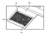
도 2는 도 1에 나타낸 디스플레이 장치의 가이드 패널 상에 가이드 홀더를 통하여 결합된 회로기판을 도시하는 사시도이다.
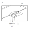
도 3은 본 발명의 제1실시예에 따른 디스플레이 장치의 제1고정부를 부분적으로 확대 도시하는 부분 확대 사시도이다.
도 4는 도 3에 나타낸 디스플레이 장치의 제1고정부에 회로기판이 결합된 상태를 도시하는 사시도이다.
도 5는 본 발명의 제2실시예에 따른 디스플레이 장치의 제1고정부를 부분적으로 확대 도시하는 부분 확대 사시도이다.
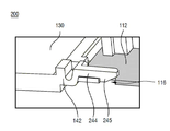
도 6은 도 1에 나타낸 디스플레이 장치의 제2고정부를 부분적으로 확대 도시하는 부분 확대 사시도이다.
110 : 디스플레이패널
120 : 방열판
130 : 가이드 패널
140 : 가이드 홀더
Claims (10)
- 디스플레이 패널;
상기 디스플레이 패널의 배면에 결합되는 방열판;
배면에 상기 디스플레이 패널로부터 연결된 회로기판이 결합되도록 결합홈이 마련되고, 상기 방열판의 배면에 결합되는 가이드 패널 및
상기 가이드 패널 상에서 상기 회로기판이 결합되는 모서리 부분에 복수개 구비되어 상기 회로기판을 탈착 가능하도록 결합시키는 가이드 홀더;
를 포함하는 디스플레이 장치. - 청구항 1에 있어서,
상기 가이드 홀더는,
상기 회로기판의 일 측면 모서리 부분을 고정하는 제1고정부와,
상기 제1고정부와 대향하도록 배치되어 상기 회로기판의 타 측면 모서리 부분을 고정하는 제2고정부를 포함하는 디스플레이 장치. - 청구항 2에 있어서,
상기 제1고정부는.
상기 결합홈 내주면에서 상기 회로기판의 일 측 상면 방향으로 구비되는 탄성부재와,
상기 탄성부재로부터 돌출되어 상기 회로기판의 상면을 수직 방향으로 고정시키는 지지부재를 포함하는 디스플레이 장치. - 청구항 3에 있어서,
상기 제1고정부는,
상기 회로기판의 모서리 부분에 형성된 안내홈에 대응하도록 상기 탄성부재의 일 측면에 돌출되어 상기 회로기판의 측면을 수평방향으로 고정시키는 가이드 돌기를 포함하는 디스플레이 장치. - 청구항 4에 있어서,
상기 지지부재와 가이드 돌기는 상기 탄성부재 상에서 서로 수직 방향으로 배치되는 디스플레이 장치. - 청구항 3에 있어서,
상기 탄성부재는,
상기 가이드 패널과 일체로 마련되며, 일 단면이 "U" 또는 "V"자 형상으로 마련되는 디스플레이 장치. - 청구항 2에 있어서,
상기 제1고정부는.
상기 결합홈 내주면에서 상기 회로기판의 상면 방향으로 구비되는 탄성부재와,
상기 탄성부재에 탄력적으로 결합되어 상기 회로기판의 상면을 가압하는 지지부재와,
상기 지지부재의 단부에서 상기 회로기판에 형성된 타공홀에 삽입되도록 돌출되는 고정돌기를 포함하는 디스플레이 장치. - 청구항 2에 있어서,
상기 제2고정부는,
상기 결합홈 내주면에서 상기 회로기판의 타 측 상면 방향으로 돌출되는 단턱을 포함하는 디스플레이 장치. - 청구항 8에 있어서,
상기 단턱은,
적어도 상기 탄성부재가 탄력적으로 유동할 수 있는 범위와 같거나 큰 폭으로 돌출되는 디스플레이 장치. - 청구항 8에 있어서,
상기 제2고정부는,
상기 단턱의 하측에서 적어도 상기 회로기판의 측면과 접촉하는 영역에 마련되는 방진부재를 포함하는 디스플레이 장치.
Priority Applications (5)
| Application Number | Priority Date | Filing Date | Title |
|---|---|---|---|
| KR1020180153656A KR102648419B1 (ko) | 2018-12-03 | 2018-12-03 | 디스플레이 장치 |
| CN201911134692.8A CN111261083B (zh) | 2018-12-03 | 2019-11-19 | 显示装置 |
| CN202310927385.5A CN117032490A (zh) | 2018-12-03 | 2019-11-19 | 显示装置 |
| US16/701,523 US11153997B2 (en) | 2018-12-03 | 2019-12-03 | Display apparatus |
| US17/479,361 US11889669B2 (en) | 2018-12-03 | 2021-09-20 | Display apparatus |
Applications Claiming Priority (1)
| Application Number | Priority Date | Filing Date | Title |
|---|---|---|---|
| KR1020180153656A KR102648419B1 (ko) | 2018-12-03 | 2018-12-03 | 디스플레이 장치 |
Publications (2)
| Publication Number | Publication Date |
|---|---|
| KR20200066920A true KR20200066920A (ko) | 2020-06-11 |
| KR102648419B1 KR102648419B1 (ko) | 2024-03-18 |
Family
ID=70848531
Family Applications (1)
| Application Number | Title | Priority Date | Filing Date |
|---|---|---|---|
| KR1020180153656A Active KR102648419B1 (ko) | 2018-12-03 | 2018-12-03 | 디스플레이 장치 |
Country Status (3)
| Country | Link |
|---|---|
| US (2) | US11153997B2 (ko) |
| KR (1) | KR102648419B1 (ko) |
| CN (2) | CN117032490A (ko) |
Cited By (1)
| Publication number | Priority date | Publication date | Assignee | Title |
|---|---|---|---|---|
| US12419018B2 (en) | 2022-12-15 | 2025-09-16 | Lg Display Co., Ltd. | Display apparatus |
Families Citing this family (2)
| Publication number | Priority date | Publication date | Assignee | Title |
|---|---|---|---|---|
| WO2023224172A1 (ko) * | 2022-05-20 | 2023-11-23 | 엘지전자 주식회사 | 디스플레이 디바이스 |
| WO2026006989A1 (en) * | 2024-07-02 | 2026-01-08 | Siemens Aktiengesellschaft | Flat-panel display |
Citations (2)
| Publication number | Priority date | Publication date | Assignee | Title |
|---|---|---|---|---|
| US20060289830A1 (en) * | 2005-06-24 | 2006-12-28 | Innolux Display Corp. | Liquid crystal display device with power connection stabilizer |
| JP2017037219A (ja) * | 2015-08-11 | 2017-02-16 | 三菱電機株式会社 | 電子機器 |
Family Cites Families (5)
| Publication number | Priority date | Publication date | Assignee | Title |
|---|---|---|---|---|
| KR101010388B1 (ko) * | 2004-04-30 | 2011-01-21 | 엘지디스플레이 주식회사 | 인쇄회로기판의 고정구조 및 그 고정방법 |
| KR101082284B1 (ko) * | 2009-09-15 | 2011-11-09 | 삼성모바일디스플레이주식회사 | 평판표시장치 |
| CN102655729A (zh) * | 2011-03-02 | 2012-09-05 | 鸿富锦精密工业(深圳)有限公司 | 便携式电子装置 |
| JP5828079B2 (ja) * | 2011-08-30 | 2015-12-02 | パナソニックIpマネジメント株式会社 | 照明装置及び照明システム |
| KR102528952B1 (ko) * | 2016-06-28 | 2023-05-03 | 엘지디스플레이 주식회사 | 디스플레이 장치 |
-
2018
- 2018-12-03 KR KR1020180153656A patent/KR102648419B1/ko active Active
-
2019
- 2019-11-19 CN CN202310927385.5A patent/CN117032490A/zh active Pending
- 2019-11-19 CN CN201911134692.8A patent/CN111261083B/zh active Active
- 2019-12-03 US US16/701,523 patent/US11153997B2/en active Active
-
2021
- 2021-09-20 US US17/479,361 patent/US11889669B2/en active Active
Patent Citations (2)
| Publication number | Priority date | Publication date | Assignee | Title |
|---|---|---|---|---|
| US20060289830A1 (en) * | 2005-06-24 | 2006-12-28 | Innolux Display Corp. | Liquid crystal display device with power connection stabilizer |
| JP2017037219A (ja) * | 2015-08-11 | 2017-02-16 | 三菱電機株式会社 | 電子機器 |
Cited By (1)
| Publication number | Priority date | Publication date | Assignee | Title |
|---|---|---|---|---|
| US12419018B2 (en) | 2022-12-15 | 2025-09-16 | Lg Display Co., Ltd. | Display apparatus |
Also Published As
| Publication number | Publication date |
|---|---|
| US20220007552A1 (en) | 2022-01-06 |
| CN117032490A (zh) | 2023-11-10 |
| KR102648419B1 (ko) | 2024-03-18 |
| CN111261083A (zh) | 2020-06-09 |
| US11889669B2 (en) | 2024-01-30 |
| US11153997B2 (en) | 2021-10-19 |
| CN111261083B (zh) | 2023-08-25 |
| US20200178425A1 (en) | 2020-06-04 |
Similar Documents
| Publication | Publication Date | Title |
|---|---|---|
| US9671630B2 (en) | Display device | |
| CN109479109B (zh) | 显示装置 | |
| CN102024390A (zh) | 图像显示装置 | |
| US9343025B2 (en) | Display device | |
| US8031291B2 (en) | Liquid crystal display and tablet computer having a chassis fastening member that receives a printed circuit board | |
| US11889669B2 (en) | Display apparatus | |
| KR100995576B1 (ko) | 액정표시장치 및 이를 갖는 타블렛 피씨 | |
| KR102656239B1 (ko) | 디스플레이 장치 | |
| KR102836436B1 (ko) | 디스플레이 장치 | |
| US20140132848A1 (en) | Illuminating device, display device, and television receiver | |
| KR101943056B1 (ko) | 커버쉴드 및 이를 포함하는 액정표시장치 | |
| KR20200075427A (ko) | 부착수단 및 이를 구비한 디스플레이 장치의 제조방법 | |
| KR20080067875A (ko) | 백라이트 어셈블리 및 이를 구비한 표시 장치 | |
| KR102579253B1 (ko) | 디스플레이 장치 | |
| KR102725764B1 (ko) | 디스플레이 장치 | |
| KR101671521B1 (ko) | 액정표시장치 | |
| KR20070081892A (ko) | 액정 표시 장치 | |
| KR100784043B1 (ko) | 평판표시장치 | |
| KR102396463B1 (ko) | 액정표시장치 | |
| KR20070051981A (ko) | 액정표시장치 및 그의 조립방법 | |
| KR20080029122A (ko) | 표시 장치 | |
| KR20080014187A (ko) | 표시 장치 | |
| KR20080073093A (ko) | 표시 장치 | |
| KR20080048778A (ko) | 표시 장치 | |
| KR20080060086A (ko) | 표시 장치 |
Legal Events
| Date | Code | Title | Description |
|---|---|---|---|
| PA0109 | Patent application |
Patent event code: PA01091R01D Comment text: Patent Application Patent event date: 20181203 |
|
| PG1501 | Laying open of application | ||
| A201 | Request for examination | ||
| PA0201 | Request for examination |
Patent event code: PA02012R01D Patent event date: 20211115 Comment text: Request for Examination of Application Patent event code: PA02011R01I Patent event date: 20181203 Comment text: Patent Application |
|
| E902 | Notification of reason for refusal | ||
| PE0902 | Notice of grounds for rejection |
Comment text: Notification of reason for refusal Patent event date: 20230817 Patent event code: PE09021S01D |
|
| E701 | Decision to grant or registration of patent right | ||
| PE0701 | Decision of registration |
Patent event code: PE07011S01D Comment text: Decision to Grant Registration Patent event date: 20231227 |
|
| GRNT | Written decision to grant | ||
| PR0701 | Registration of establishment |
Comment text: Registration of Establishment Patent event date: 20240312 Patent event code: PR07011E01D |
|
| PR1002 | Payment of registration fee |
Payment date: 20240313 End annual number: 3 Start annual number: 1 |
|
| PG1601 | Publication of registration |