KR20200067754A - 멀티 전자 빔 검사 장치 - Google Patents
멀티 전자 빔 검사 장치 Download PDFInfo
- Publication number
- KR20200067754A KR20200067754A KR1020190154483A KR20190154483A KR20200067754A KR 20200067754 A KR20200067754 A KR 20200067754A KR 1020190154483 A KR1020190154483 A KR 1020190154483A KR 20190154483 A KR20190154483 A KR 20190154483A KR 20200067754 A KR20200067754 A KR 20200067754A
- Authority
- KR
- South Korea
- Prior art keywords
- electron beam
- lens
- substrate
- holes
- electron
- Prior art date
- Legal status (The legal status is an assumption and is not a legal conclusion. Google has not performed a legal analysis and makes no representation as to the accuracy of the status listed.)
- Granted
Links
Images


Classifications
-
- H—ELECTRICITY
- H01—ELECTRIC ELEMENTS
- H01J—ELECTRIC DISCHARGE TUBES OR DISCHARGE LAMPS
- H01J37/00—Discharge tubes with provision for introducing objects or material to be exposed to the discharge, e.g. for the purpose of examination or processing thereof
- H01J37/02—Details
- H01J37/04—Arrangements of electrodes and associated parts for generating or controlling the discharge, e.g. electron-optical arrangement or ion-optical arrangement
- H01J37/10—Lenses
- H01J37/145—Combinations of electrostatic and magnetic lenses
-
- H—ELECTRICITY
- H01—ELECTRIC ELEMENTS
- H01J—ELECTRIC DISCHARGE TUBES OR DISCHARGE LAMPS
- H01J37/00—Discharge tubes with provision for introducing objects or material to be exposed to the discharge, e.g. for the purpose of examination or processing thereof
- H01J37/30—Electron-beam or ion-beam tubes for localised treatment of objects
- H01J37/317—Electron-beam or ion-beam tubes for localised treatment of objects for changing properties of the objects or for applying thin layers thereon, e.g. for ion implantation
- H01J37/3174—Particle-beam lithography, e.g. electron beam lithography
- H01J37/3177—Multi-beam, e.g. fly's eye, comb probe
-
- H—ELECTRICITY
- H01—ELECTRIC ELEMENTS
- H01J—ELECTRIC DISCHARGE TUBES OR DISCHARGE LAMPS
- H01J37/00—Discharge tubes with provision for introducing objects or material to be exposed to the discharge, e.g. for the purpose of examination or processing thereof
- H01J37/02—Details
- H01J37/04—Arrangements of electrodes and associated parts for generating or controlling the discharge, e.g. electron-optical arrangement or ion-optical arrangement
- H01J37/10—Lenses
- H01J37/12—Lenses electrostatic
-
- H—ELECTRICITY
- H01—ELECTRIC ELEMENTS
- H01J—ELECTRIC DISCHARGE TUBES OR DISCHARGE LAMPS
- H01J37/00—Discharge tubes with provision for introducing objects or material to be exposed to the discharge, e.g. for the purpose of examination or processing thereof
- H01J37/02—Details
- H01J37/04—Arrangements of electrodes and associated parts for generating or controlling the discharge, e.g. electron-optical arrangement or ion-optical arrangement
- H01J37/10—Lenses
- H01J37/14—Lenses magnetic
- H01J37/141—Electromagnetic lenses
-
- H—ELECTRICITY
- H01—ELECTRIC ELEMENTS
- H01J—ELECTRIC DISCHARGE TUBES OR DISCHARGE LAMPS
- H01J37/00—Discharge tubes with provision for introducing objects or material to be exposed to the discharge, e.g. for the purpose of examination or processing thereof
- H01J37/02—Details
- H01J37/20—Means for supporting or positioning the object or the material; Means for adjusting diaphragms or lenses associated with the support
-
- H—ELECTRICITY
- H01—ELECTRIC ELEMENTS
- H01J—ELECTRIC DISCHARGE TUBES OR DISCHARGE LAMPS
- H01J37/00—Discharge tubes with provision for introducing objects or material to be exposed to the discharge, e.g. for the purpose of examination or processing thereof
- H01J37/26—Electron or ion microscopes; Electron or ion diffraction tubes
- H01J37/28—Electron or ion microscopes; Electron or ion diffraction tubes with scanning beams
-
- H—ELECTRICITY
- H01—ELECTRIC ELEMENTS
- H01J—ELECTRIC DISCHARGE TUBES OR DISCHARGE LAMPS
- H01J2237/00—Discharge tubes exposing object to beam, e.g. for analysis treatment, etching, imaging
- H01J2237/10—Lenses
- H01J2237/12—Lenses electrostatic
- H01J2237/121—Lenses electrostatic characterised by shape
-
- H—ELECTRICITY
- H01—ELECTRIC ELEMENTS
- H01J—ELECTRIC DISCHARGE TUBES OR DISCHARGE LAMPS
- H01J2237/00—Discharge tubes exposing object to beam, e.g. for analysis treatment, etching, imaging
- H01J2237/10—Lenses
- H01J2237/14—Lenses magnetic
-
- H—ELECTRICITY
- H01—ELECTRIC ELEMENTS
- H01J—ELECTRIC DISCHARGE TUBES OR DISCHARGE LAMPS
- H01J2237/00—Discharge tubes exposing object to beam, e.g. for analysis treatment, etching, imaging
- H01J2237/244—Detection characterized by the detecting means
- H01J2237/2443—Scintillation detectors
Landscapes
- Chemical & Material Sciences (AREA)
- Analytical Chemistry (AREA)
- Physics & Mathematics (AREA)
- Electromagnetism (AREA)
- Testing Or Measuring Of Semiconductors Or The Like (AREA)
Abstract
Description
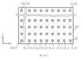
도 2는, 실시 형태의 성형 애퍼처 어레이 기판의 구성을 나타내는 개념도이다.
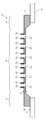
도 3은, 실시 형태에 있어서의 블랭킹 애퍼처 어레이 기구의 구성을 나타내는 단면도이다.
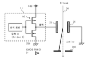
도 4는, 실시 형태의 개별 블랭킹 기구의 일예를 나타내는 도면이다.
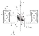
도 5는, 실시 형태의 멀티 전자 빔 검사 장치가 구비하는 정전 렌즈와 전자기 렌즈의 모식 단면도이다.
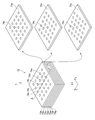
도 6은, 실시 형태의 정전 렌즈의 모식 사시도이다.
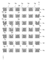
도 7은, 실시 형태의 정전 렌즈를 구성하는 절연판 및 도전막의 일예의 모식도이다.
도 8은, 실시 형태의 정전 렌즈를 구성하는 절연판 및 도전막의 모식 단면도이다.
Claims (8)
- 기판에 멀티 전자 빔을 조사하는 조사원과,
상기 기판을 재치하는 스테이지와,
상기 조사원과 상기 스테이지의 사이에 설치되어, 상기 멀티 전자 빔이 통과 가능한 렌즈 자기장을 발생하는 전자기 렌즈와,
상기 렌즈 자기장 중에 설치되어, 상기 멀티 전자 빔의 각각이 통과 가능한 복수의 관통 홀과, 상기 복수의 관통 홀의 벽면에 각각 설치된 복수의 전극을 가지고, 상기 멀티 전자 빔의 궤도 중심 축으로부터 이간하여 설치된 상기 관통 홀의 배치는 나선 형상을 가지는 정전 렌즈와,
상기 복수의 전극에 접속된 전원
을 구비하는 멀티 전자 빔 검사 장치. - 제1항에 있어서,
상기 나선 형상의 축은, 상기 궤도 중심 축에 평행하게 설치되어 있는 멀티 전자 빔 검사 장치. - 제1항에 있어서,
상기 전원은 상기 복수의 전극의 각각에 상이한 전압을 인가하는 멀티 전자 빔 검사 장치. - 제1항에 있어서,
상기 궤도 중심 축에 평행한 방향의 상기 복수의 전극의 길이는 서로 상이한 멀티 전자 빔 검사 장치. - 제1항에 있어서,
상기 렌즈 자기장의 중심은 기판면의 높이 위치에 배치되어 있는 멀티 전자 빔 검사 장치. - 제1항에 있어서,
상기 정전 렌즈는, 각각이 복수의 관통 홀을 가지는 복수의 절연판을 가지는 멀티 전자 빔 검사 장치. - 제1항에 있어서,
상기 정전 렌즈의, 상기 궤도 중심 축에 평행한 방향의 두께는, 10mm 이상 20mm 이하인 멀티 전자 빔 검사 장치. - 제1항에 있어서,
상기 관통 홀의 나선 형상의 회전각은, 30 도 이상 40 도 이하인 멀티 전자 빔 검사 장치.
Applications Claiming Priority (2)
| Application Number | Priority Date | Filing Date | Title |
|---|---|---|---|
| JPJP-P-2018-227658 | 2018-12-04 | ||
| JP2018227658A JP7194572B2 (ja) | 2018-12-04 | 2018-12-04 | マルチ電子ビーム検査装置 |
Publications (2)
| Publication Number | Publication Date |
|---|---|
| KR20200067754A true KR20200067754A (ko) | 2020-06-12 |
| KR102375499B1 KR102375499B1 (ko) | 2022-03-17 |
Family
ID=70849314
Family Applications (1)
| Application Number | Title | Priority Date | Filing Date |
|---|---|---|---|
| KR1020190154483A Active KR102375499B1 (ko) | 2018-12-04 | 2019-11-27 | 멀티 전자 빔 검사 장치 |
Country Status (4)
| Country | Link |
|---|---|
| US (1) | US10950410B2 (ko) |
| JP (1) | JP7194572B2 (ko) |
| KR (1) | KR102375499B1 (ko) |
| TW (1) | TWI739208B (ko) |
Cited By (1)
| Publication number | Priority date | Publication date | Assignee | Title |
|---|---|---|---|---|
| KR20220036326A (ko) * | 2020-09-15 | 2022-03-22 | 가부시키가이샤 뉴플레어 테크놀로지 | 멀티빔 전자총을 위한 저-블러 정전 전달 렌즈 |
Families Citing this family (11)
| Publication number | Priority date | Publication date | Assignee | Title |
|---|---|---|---|---|
| JP7624829B2 (ja) | 2020-12-15 | 2025-01-31 | 株式会社ニューフレアテクノロジー | 電子ビーム照射装置及び電子ビーム照射方法 |
| JP7492929B2 (ja) * | 2021-02-19 | 2024-05-30 | 株式会社東芝 | 半導体装置、荷電粒子ビーム描画装置及びマルチ荷電粒子ビーム照射装置 |
| JP7582000B2 (ja) * | 2021-03-22 | 2024-11-13 | 株式会社ニューフレアテクノロジー | マルチ荷電粒子ビーム描画装置及びその調整方法 |
| JP2022174714A (ja) * | 2021-05-11 | 2022-11-24 | 株式会社ニューフレアテクノロジー | マルチ2次電子ビームの位置合わせ方法、マルチ2次電子ビームの位置合わせ装置、及び電子ビーム検査装置 |
| JP2023046921A (ja) * | 2021-09-24 | 2023-04-05 | 株式会社ニューフレアテクノロジー | マルチ電子ビーム画像取得装置、マルチ電子ビーム検査装置、及びマルチ電子ビーム画像取得方法 |
| JP7647483B2 (ja) * | 2021-10-13 | 2025-03-18 | 株式会社ニューフレアテクノロジー | 電子ビーム検査装置 |
| WO2024009913A1 (ja) * | 2022-07-06 | 2024-01-11 | 株式会社ニューフレアテクノロジー | マルチ電子ビーム画像取得装置、マルチ電子ビーム画像取得方法、電子ビーム画像取得装置、及び電子ビーム画像取得方法 |
| KR20240007062A (ko) * | 2022-07-07 | 2024-01-16 | 가부시키가이샤 뉴플레어 테크놀로지 | 실장 기판, 블랭킹 애퍼처 어레이 칩, 블랭킹 애퍼처 어레이 시스템 및 멀티 하전 입자 빔 조사 장치 |
| TWI870972B (zh) * | 2022-09-26 | 2025-01-21 | 德商卡爾蔡司多重掃描電子顯微鏡有限公司 | 帶電粒子束裝置的擾動補償 |
| WO2024154183A1 (ja) * | 2023-01-16 | 2024-07-25 | 株式会社ニューフレアテクノロジー | マルチ荷電粒子ビーム描画装置 |
| KR102839119B1 (ko) * | 2023-01-16 | 2025-07-28 | 가부시키가이샤 뉴플레어 테크놀로지 | 멀티 하전 입자 빔 묘화 장치 |
Citations (4)
| Publication number | Priority date | Publication date | Assignee | Title |
|---|---|---|---|---|
| JPS63228551A (ja) * | 1987-03-05 | 1988-09-22 | エヌ・ベー・フィリップス・フルーイランペンファブリケン | 陰極線管の磁界集束レンズ |
| US8362427B2 (en) * | 2011-03-17 | 2013-01-29 | Kabushiki Kaisha Toshiba | Electron beam irradiation apparatus and electron beam drawing apparatus |
| KR20160125313A (ko) * | 2015-04-21 | 2016-10-31 | 가부시키가이샤 뉴플레어 테크놀로지 | 하전 입자빔 묘화 장치 및 하전 입자빔 묘화 방법 |
| KR20170085433A (ko) * | 2016-01-14 | 2017-07-24 | 가부시키가이샤 뉴플레어 테크놀로지 | 멀티 하전 입자 빔 묘화 방법 및 멀티 하전 입자 빔 묘화 장치 |
Family Cites Families (12)
| Publication number | Priority date | Publication date | Assignee | Title |
|---|---|---|---|---|
| JPS61101944A (ja) | 1984-10-25 | 1986-05-20 | Nippon Telegr & Teleph Corp <Ntt> | 荷電粒子ビ−ム用集束装置 |
| WO1988004104A1 (fr) * | 1986-11-28 | 1988-06-02 | Nippon Telegraph And Telephone Corporation | Appareil d'observation utilisant des faisceaux de particules chargees et procede d'observation de surfaces utilisant des faisceaux de particules chargees |
| US5362964A (en) * | 1993-07-30 | 1994-11-08 | Electroscan Corporation | Environmental scanning electron microscope |
| JP3455071B2 (ja) * | 1997-07-29 | 2003-10-06 | 株式会社東芝 | 荷電粒子ビーム照射装置 |
| EP2559534B1 (en) * | 2008-09-26 | 2023-10-25 | Raytheon Technologies Corporation | Composition and method for casting manufacturing |
| JP2011023126A (ja) * | 2009-07-13 | 2011-02-03 | Kobe Univ | 荷電粒子線照射装置、描画装置、分析顕微鏡、荷電粒子線出射装置および荷電粒子線用のレンズ装置 |
| DE102010041156B9 (de) * | 2010-09-21 | 2018-01-25 | Carl Zeiss Microscopy Gmbh | Blendeneinheit für ein Teilchenstrahlgerät sowie Teilchenstrahlgerät |
| TWI593961B (zh) | 2010-12-15 | 2017-08-01 | 日立全球先端科技股份有限公司 | Charged particle line application device, and irradiation method |
| EP2681755B1 (en) * | 2011-03-04 | 2017-06-07 | PerkinElmer Health Sciences, Inc. | Electrostatic lenses and systems including the same |
| JP6080540B2 (ja) | 2012-12-26 | 2017-02-15 | 株式会社ニューフレアテクノロジー | 荷電粒子ビーム描画装置 |
| JP6781582B2 (ja) * | 2016-07-25 | 2020-11-04 | 株式会社ニューフレアテクノロジー | 電子ビーム検査装置及び電子ビーム検査方法 |
| DE102018115012A1 (de) | 2018-06-21 | 2019-12-24 | Carl Zeiss Microscopy Gmbh | Teilchenstrahlsystem |
-
2018
- 2018-12-04 JP JP2018227658A patent/JP7194572B2/ja active Active
-
2019
- 2019-11-13 TW TW108141135A patent/TWI739208B/zh active
- 2019-11-18 US US16/686,316 patent/US10950410B2/en active Active
- 2019-11-27 KR KR1020190154483A patent/KR102375499B1/ko active Active
Patent Citations (4)
| Publication number | Priority date | Publication date | Assignee | Title |
|---|---|---|---|---|
| JPS63228551A (ja) * | 1987-03-05 | 1988-09-22 | エヌ・ベー・フィリップス・フルーイランペンファブリケン | 陰極線管の磁界集束レンズ |
| US8362427B2 (en) * | 2011-03-17 | 2013-01-29 | Kabushiki Kaisha Toshiba | Electron beam irradiation apparatus and electron beam drawing apparatus |
| KR20160125313A (ko) * | 2015-04-21 | 2016-10-31 | 가부시키가이샤 뉴플레어 테크놀로지 | 하전 입자빔 묘화 장치 및 하전 입자빔 묘화 방법 |
| KR20170085433A (ko) * | 2016-01-14 | 2017-07-24 | 가부시키가이샤 뉴플레어 테크놀로지 | 멀티 하전 입자 빔 묘화 방법 및 멀티 하전 입자 빔 묘화 장치 |
Cited By (1)
| Publication number | Priority date | Publication date | Assignee | Title |
|---|---|---|---|---|
| KR20220036326A (ko) * | 2020-09-15 | 2022-03-22 | 가부시키가이샤 뉴플레어 테크놀로지 | 멀티빔 전자총을 위한 저-블러 정전 전달 렌즈 |
Also Published As
| Publication number | Publication date |
|---|---|
| TWI739208B (zh) | 2021-09-11 |
| KR102375499B1 (ko) | 2022-03-17 |
| JP7194572B2 (ja) | 2022-12-22 |
| TW202038284A (zh) | 2020-10-16 |
| US20200176216A1 (en) | 2020-06-04 |
| JP2020091986A (ja) | 2020-06-11 |
| US10950410B2 (en) | 2021-03-16 |
Similar Documents
| Publication | Publication Date | Title |
|---|---|---|
| KR102375499B1 (ko) | 멀티 전자 빔 검사 장치 | |
| TWI745687B (zh) | 多電子束影像取得裝置以及多電子束光學系統的定位方法 | |
| JP6966255B2 (ja) | 画像取得装置の光学系調整方法 | |
| US20090146082A1 (en) | Pattern Lock System for Particle-Beam Exposure Apparatus | |
| KR102532712B1 (ko) | 전자 광학계 및 멀티 빔 화상 취득 장치 | |
| TWI772803B (zh) | 像差修正器以及多電子束照射裝置 | |
| JP2003202217A (ja) | パターン欠陥検査方法及びパターン欠陥検査装置 | |
| KR20190131435A (ko) | 멀티 전자 빔 화상 취득 장치 및 멀티 전자 빔 화상 취득 방법 | |
| JP6966319B2 (ja) | マルチビーム画像取得装置及びマルチビーム画像取得方法 | |
| KR102553520B1 (ko) | 멀티 하전 입자 빔 조사 장치 및 멀티 하전 입자 빔 검사 장치 | |
| TWI834161B (zh) | 多電子束圖像取得裝置及多電子束圖像取得方法 | |
| JP2004014485A (ja) | ウェハ欠陥検査方法及びウェハ欠陥検査装置 | |
| KR20220106057A (ko) | 멀티 빔 화상 취득 장치 및 멀티 빔 화상 취득 방법 | |
| US20230077403A1 (en) | Multi-electron beam image acquisition apparatus, and multi-electron beam image acquisition method | |
| JP2005091342A (ja) | 試料欠陥検査装置及び方法並びに該欠陥検査装置及び方法を用いたデバイス製造方法 | |
| WO2022091475A1 (ja) | ウィーンフィルタ及びマルチ電子ビーム検査装置 | |
| TW202441287A (zh) | 電子線遮罩檢查裝置 | |
| KR102901663B1 (ko) | 전자 렌즈, 주사형 전자 현미경 및 전자 빔 검사 장치 | |
| JP2005164608A (ja) | パターン欠陥検査方法及びパターン欠陥検査装置 | |
| TW202527014A (zh) | 電磁透鏡及多電子束照射裝置 | |
| JP2022154067A (ja) | 電子ビームの軌道軸調整方法及びマルチビーム画像取得装置 | |
| JP2020020710A (ja) | 検査装置 | |
| WO2021039419A1 (ja) | 電子銃及び電子ビーム照射装置 | |
| JP2005129546A (ja) | パターン欠陥検査方法及びパターン欠陥検査装置 |
Legal Events
| Date | Code | Title | Description |
|---|---|---|---|
| PA0109 | Patent application |
Patent event code: PA01091R01D Comment text: Patent Application Patent event date: 20191127 |
|
| PA0201 | Request for examination | ||
| PG1501 | Laying open of application | ||
| E902 | Notification of reason for refusal | ||
| PE0902 | Notice of grounds for rejection |
Comment text: Notification of reason for refusal Patent event date: 20210616 Patent event code: PE09021S01D |
|
| E701 | Decision to grant or registration of patent right | ||
| PE0701 | Decision of registration |
Patent event code: PE07011S01D Comment text: Decision to Grant Registration Patent event date: 20211220 |
|
| GRNT | Written decision to grant | ||
| PR0701 | Registration of establishment |
Comment text: Registration of Establishment Patent event date: 20220314 Patent event code: PR07011E01D |
|
| PR1002 | Payment of registration fee |
Payment date: 20220315 End annual number: 3 Start annual number: 1 |
|
| PG1601 | Publication of registration | ||
| PR1001 | Payment of annual fee |
Payment date: 20250218 Start annual number: 4 End annual number: 4 |