KR20200068576A - 열처리 장치 및 열처리 방법 - Google Patents
열처리 장치 및 열처리 방법 Download PDFInfo
- Publication number
- KR20200068576A KR20200068576A KR1020190151055A KR20190151055A KR20200068576A KR 20200068576 A KR20200068576 A KR 20200068576A KR 1020190151055 A KR1020190151055 A KR 1020190151055A KR 20190151055 A KR20190151055 A KR 20190151055A KR 20200068576 A KR20200068576 A KR 20200068576A
- Authority
- KR
- South Korea
- Prior art keywords
- temperature
- substrate
- heating
- wafer
- hot plate
- Prior art date
- Legal status (The legal status is an assumption and is not a legal conclusion. Google has not performed a legal analysis and makes no representation as to the accuracy of the status listed.)
- Granted
Links
Images




Classifications
-
- H—ELECTRICITY
- H10—SEMICONDUCTOR DEVICES; ELECTRIC SOLID-STATE DEVICES NOT OTHERWISE PROVIDED FOR
- H10P—GENERIC PROCESSES OR APPARATUS FOR THE MANUFACTURE OR TREATMENT OF DEVICES COVERED BY CLASS H10
- H10P95/00—Generic processes or apparatus for manufacture or treatments not covered by the other groups of this subclass
-
- G—PHYSICS
- G03—PHOTOGRAPHY; CINEMATOGRAPHY; ANALOGOUS TECHNIQUES USING WAVES OTHER THAN OPTICAL WAVES; ELECTROGRAPHY; HOLOGRAPHY
- G03F—PHOTOMECHANICAL PRODUCTION OF TEXTURED OR PATTERNED SURFACES, e.g. FOR PRINTING, FOR PROCESSING OF SEMICONDUCTOR DEVICES; MATERIALS THEREFOR; ORIGINALS THEREFOR; APPARATUS SPECIALLY ADAPTED THEREFOR
- G03F7/00—Photomechanical, e.g. photolithographic, production of textured or patterned surfaces, e.g. printing surfaces; Materials therefor, e.g. comprising photoresists; Apparatus specially adapted therefor
- G03F7/002—Photomechanical, e.g. photolithographic, production of textured or patterned surfaces, e.g. printing surfaces; Materials therefor, e.g. comprising photoresists; Apparatus specially adapted therefor using materials containing microcapsules; Preparing or processing such materials, e.g. by pressure; Devices or apparatus specially designed therefor
- G03F7/0022—Devices or apparatus
- G03F7/0032—Devices or apparatus characterised by heat providing or glossing means
-
- G—PHYSICS
- G03—PHOTOGRAPHY; CINEMATOGRAPHY; ANALOGOUS TECHNIQUES USING WAVES OTHER THAN OPTICAL WAVES; ELECTROGRAPHY; HOLOGRAPHY
- G03F—PHOTOMECHANICAL PRODUCTION OF TEXTURED OR PATTERNED SURFACES, e.g. FOR PRINTING, FOR PROCESSING OF SEMICONDUCTOR DEVICES; MATERIALS THEREFOR; ORIGINALS THEREFOR; APPARATUS SPECIALLY ADAPTED THEREFOR
- G03F7/00—Photomechanical, e.g. photolithographic, production of textured or patterned surfaces, e.g. printing surfaces; Materials therefor, e.g. comprising photoresists; Apparatus specially adapted therefor
- G03F7/26—Processing photosensitive materials; Apparatus therefor
- G03F7/40—Treatment after imagewise removal, e.g. baking
-
- G—PHYSICS
- G03—PHOTOGRAPHY; CINEMATOGRAPHY; ANALOGOUS TECHNIQUES USING WAVES OTHER THAN OPTICAL WAVES; ELECTROGRAPHY; HOLOGRAPHY
- G03F—PHOTOMECHANICAL PRODUCTION OF TEXTURED OR PATTERNED SURFACES, e.g. FOR PRINTING, FOR PROCESSING OF SEMICONDUCTOR DEVICES; MATERIALS THEREFOR; ORIGINALS THEREFOR; APPARATUS SPECIALLY ADAPTED THEREFOR
- G03F7/00—Photomechanical, e.g. photolithographic, production of textured or patterned surfaces, e.g. printing surfaces; Materials therefor, e.g. comprising photoresists; Apparatus specially adapted therefor
- G03F7/70—Microphotolithographic exposure; Apparatus therefor
- G03F7/70691—Handling of masks or workpieces
- G03F7/70733—Handling masks and workpieces, e.g. exchange of workpiece or mask, transport of workpiece or mask
-
- G—PHYSICS
- G03—PHOTOGRAPHY; CINEMATOGRAPHY; ANALOGOUS TECHNIQUES USING WAVES OTHER THAN OPTICAL WAVES; ELECTROGRAPHY; HOLOGRAPHY
- G03F—PHOTOMECHANICAL PRODUCTION OF TEXTURED OR PATTERNED SURFACES, e.g. FOR PRINTING, FOR PROCESSING OF SEMICONDUCTOR DEVICES; MATERIALS THEREFOR; ORIGINALS THEREFOR; APPARATUS SPECIALLY ADAPTED THEREFOR
- G03F7/00—Photomechanical, e.g. photolithographic, production of textured or patterned surfaces, e.g. printing surfaces; Materials therefor, e.g. comprising photoresists; Apparatus specially adapted therefor
- G03F7/70—Microphotolithographic exposure; Apparatus therefor
- G03F7/708—Construction of apparatus, e.g. environment aspects, hygiene aspects or materials
- G03F7/70858—Environment aspects, e.g. pressure of beam-path gas, temperature
- G03F7/70866—Environment aspects, e.g. pressure of beam-path gas, temperature of mask or workpiece
- G03F7/70875—Temperature, e.g. temperature control of masks or workpieces via control of stage temperature
-
- H01L21/324—
-
- H01L21/67103—
-
- H01L21/67248—
-
- H01L21/67742—
-
- H—ELECTRICITY
- H10—SEMICONDUCTOR DEVICES; ELECTRIC SOLID-STATE DEVICES NOT OTHERWISE PROVIDED FOR
- H10P—GENERIC PROCESSES OR APPARATUS FOR THE MANUFACTURE OR TREATMENT OF DEVICES COVERED BY CLASS H10
- H10P72/00—Handling or holding of wafers, substrates or devices during manufacture or treatment thereof
- H10P72/04—Apparatus for manufacture or treatment
- H10P72/0431—Apparatus for thermal treatment
-
- H—ELECTRICITY
- H10—SEMICONDUCTOR DEVICES; ELECTRIC SOLID-STATE DEVICES NOT OTHERWISE PROVIDED FOR
- H10P—GENERIC PROCESSES OR APPARATUS FOR THE MANUFACTURE OR TREATMENT OF DEVICES COVERED BY CLASS H10
- H10P72/00—Handling or holding of wafers, substrates or devices during manufacture or treatment thereof
- H10P72/04—Apparatus for manufacture or treatment
- H10P72/0431—Apparatus for thermal treatment
- H10P72/0432—Apparatus for thermal treatment mainly by conduction
-
- H—ELECTRICITY
- H10—SEMICONDUCTOR DEVICES; ELECTRIC SOLID-STATE DEVICES NOT OTHERWISE PROVIDED FOR
- H10P—GENERIC PROCESSES OR APPARATUS FOR THE MANUFACTURE OR TREATMENT OF DEVICES COVERED BY CLASS H10
- H10P72/00—Handling or holding of wafers, substrates or devices during manufacture or treatment thereof
- H10P72/06—Apparatus for monitoring, sorting, marking, testing or measuring
- H10P72/0602—Temperature monitoring
-
- H—ELECTRICITY
- H10—SEMICONDUCTOR DEVICES; ELECTRIC SOLID-STATE DEVICES NOT OTHERWISE PROVIDED FOR
- H10P—GENERIC PROCESSES OR APPARATUS FOR THE MANUFACTURE OR TREATMENT OF DEVICES COVERED BY CLASS H10
- H10P72/00—Handling or holding of wafers, substrates or devices during manufacture or treatment thereof
- H10P72/30—Handling or holding of wafers, substrates or devices during manufacture or treatment thereof for conveying, e.g. between different workstations
- H10P72/33—Handling or holding of wafers, substrates or devices during manufacture or treatment thereof for conveying, e.g. between different workstations into and out of processing chamber
- H10P72/3302—Mechanical parts of transfer devices
-
- H—ELECTRICITY
- H10—SEMICONDUCTOR DEVICES; ELECTRIC SOLID-STATE DEVICES NOT OTHERWISE PROVIDED FOR
- H10P—GENERIC PROCESSES OR APPARATUS FOR THE MANUFACTURE OR TREATMENT OF DEVICES COVERED BY CLASS H10
- H10P95/00—Generic processes or apparatus for manufacture or treatments not covered by the other groups of this subclass
- H10P95/90—Thermal treatments, e.g. annealing or sintering
Landscapes
- General Physics & Mathematics (AREA)
- Physics & Mathematics (AREA)
- Health & Medical Sciences (AREA)
- Engineering & Computer Science (AREA)
- Life Sciences & Earth Sciences (AREA)
- Toxicology (AREA)
- Atmospheric Sciences (AREA)
- Environmental & Geological Engineering (AREA)
- Epidemiology (AREA)
- Public Health (AREA)
- Exposure Of Semiconductors, Excluding Electron Or Ion Beam Exposure (AREA)
- Container, Conveyance, Adherence, Positioning, Of Wafer (AREA)
- Photosensitive Polymer And Photoresist Processing (AREA)
- Robotics (AREA)
Abstract
Description
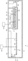
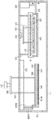
도 2는 상기 열처리 장치를 도시하는 평면도이다.
도 3은 상기 열처리 장치에 마련되는 제어부를 도시하는 구성도이다.
도 4는 상기 열처리 장치의 작용을 도시하는 설명도이다.
도 5는 상기 열처리 장치의 작용을 도시하는 설명도이다.
도 6은 상기 열처리 장치의 작용을 도시하는 설명도이다.
도 7은 상기 열처리 장치의 작용을 도시하는 설명도이다.
도 8은 상기 열처리 장치의 작용을 도시하는 설명도이다.
도 9는 상기 열처리 장치의 작용을 도시하는 설명도이다.
도 10은 본 실시 형태에 관한 열처리 장치의 다른 예를 도시하는 종단 측면도이다.
도 11은 열처리 장치의 또 다른 예에 마련되는 제어부를 도시하는 구성도이다.
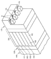
도 12는 상기 열처리 장치가 마련되는 도포, 현상 장치를 도시하는 사시도이다.
도 13은 상기 도포, 현상 장치의 평면도이다.
Claims (11)
- 적재된 기판을 제1 온도로 가열하는 열판과,
상기 기판을 지지하는 지지부를 구비하고, 상기 열판의 상방 영역과 당해 상방 영역으로부터 횡방향으로 벗어난 외측 영역 사이에서 당해 기판을 반송하는 반송체와,
상기 상방 영역에 있어서의 상기 반송체와 상기 열판 사이에서 상기 기판을 전달하는 전달 기구와,
상기 외측 영역에 있어서 상기 지지부에 지지된 상기 열판에 의한 가열 전의 기판을, 상기 제1 온도보다도 낮은 제2 온도로 가열하는 가열 기구와,
상기 열판에서 가열 완료되어 상기 외측 영역으로 반송하기 위해 상기 지지부에 지지된 상기 기판이 상기 제2 온도보다도 낮은 제3 온도로 되도록 냉각하는 냉각 기구와,
제어 신호를 출력하는 제어부
를 구비하는, 열처리 장치. - 제1항에 있어서, 상기 기판에는 노광 후이고 현상 전인 레지스트막이 형성되어 있는, 열처리 장치.
- 제1항에 있어서, 상기 지지부는 상기 가열 기구와 상기 냉각 기구에 공용되고,
상기 가열 기구 및 상기 냉각 기구는, 지지된 상기 기판이 상기 제2 온도로 되도록 상기 지지부를 가열하는 가열 상태와, 지지된 상기 기판이 상기 제3 온도로 되도록 상기 지지부를 냉각하는 냉각 상태를 서로 전환하는, 열처리 장치. - 제3항에 있어서, 상기 지지부는 펠티에 소자에 의해 구성되고,
상기 가열 기구 및 냉각 기구는 당해 펠티에 소자에 공급하는 전류의 방향을 전환함으로써 상기 가열 상태와 상기 냉각 상태를 서로 전환하는 전환 기구에 의해 구성되는, 열처리 장치. - 제3항에 있어서,
상기 기판이 상기 지지부에 지지됨과 동시이거나 지지된 후에, 당해 기판을 상기 제2 온도로 하기 위해 상기 냉각 상태로부터 상기 가열 상태로의 전환이 행해지도록 상기 제어 신호가 출력되는, 열처리 장치. - 제3항에 있어서,
상기 냉각 상태로부터 상기 가열 상태로 전환되는 타이밍은, 상기 기판을 지지하는 상기 반송체가 상기 상방 영역에 위치하는 예정 타이밍에 따른 타이밍으로 되도록 상기 제어 신호가 출력되는, 열처리 장치. - 제3항에 있어서,
당해 제어부는, 상기 지지부에 적재되기 전의 상기 기판의 온도에 대한 정보를 취득하고,
상기 기판이 반송될 때의 상기 지지부의 온도가, 당해 기판의 온도에 대응하는 온도로 되도록 제어 신호를 출력하는, 열처리 장치. - 제3항 내지 제7항 중 어느 한 항에 있어서,
상기 기판이 상기 열판에 적재되어 있는 동안, 상기 지지부가 상기 냉각 상태로 되어 강온되도록 제어 신호를 출력하는, 열처리 장치. - 제1항 또는 제2항에 있어서, 상기 반송체는,
각각 상기 지지부를 구비한 서로 별체의 제1 반송체와, 제2 반송체를 구비하고,
상기 가열 기구, 상기 냉각 기구에 의해 상기 제1 반송체의 지지부의 온도, 상기 제2 반송체의 온도가 각각 조정되는, 열처리 장치. - 제1항 내지 제7항 중 어느 한 항에 있어서, 상기 제2 온도는 20℃ 내지 70℃인, 열처리 장치.
- 열판에 적재된 기판을 제1 온도로 가열하는 공정과,
상기 기판을 지지하는 지지부를 구비하고, 상기 열판의 상방 영역과 당해 상방 영역으로부터 횡방향으로 벗어난 외측 영역 사이에서 당해 기판을 반송하는 공정과,
상기 상방 영역에 있어서의 상기 반송체와 상기 열판 사이에서 상기 기판을 전달하는 공정과,
상기 외측 영역에 있어서 상기 지지부에 지지된 상기 열판에 의한 가열 전의 기판을, 상기 제1 온도보다도 낮은 제2 온도로 가열하는 공정과,
상기 열판에서 가열 완료되어 상기 외측 영역으로 반송하기 위해 상기 지지부에 지지된 상기 기판이 상기 제2 온도보다도 낮은 제3 온도로 되도록 냉각하는 공정을 포함하는, 열처리 방법.
Applications Claiming Priority (2)
| Application Number | Priority Date | Filing Date | Title |
|---|---|---|---|
| JPJP-P-2018-228381 | 2018-12-05 | ||
| JP2018228381A JP7200638B2 (ja) | 2018-12-05 | 2018-12-05 | 熱処理装置及び熱処理方法 |
Publications (2)
| Publication Number | Publication Date |
|---|---|
| KR20200068576A true KR20200068576A (ko) | 2020-06-15 |
| KR102931410B1 KR102931410B1 (ko) | 2026-02-26 |
Family
ID=71000039
Family Applications (1)
| Application Number | Title | Priority Date | Filing Date |
|---|---|---|---|
| KR1020190151055A Active KR102931410B1 (ko) | 2018-12-05 | 2019-11-22 | 열처리 장치 및 열처리 방법 |
Country Status (4)
| Country | Link |
|---|---|
| JP (1) | JP7200638B2 (ko) |
| KR (1) | KR102931410B1 (ko) |
| CN (1) | CN111276396B (ko) |
| TW (1) | TWI830816B (ko) |
Families Citing this family (1)
| Publication number | Priority date | Publication date | Assignee | Title |
|---|---|---|---|---|
| CN115376978B (zh) * | 2022-07-05 | 2023-11-24 | 南京原磊纳米材料有限公司 | 多片式晶圆传输冷却机构 |
Citations (1)
| Publication number | Priority date | Publication date | Assignee | Title |
|---|---|---|---|---|
| JP2005150696A (ja) | 2003-10-22 | 2005-06-09 | Tokyo Electron Ltd | 熱処理装置および熱処理方法 |
Family Cites Families (11)
| Publication number | Priority date | Publication date | Assignee | Title |
|---|---|---|---|---|
| JP3525022B2 (ja) * | 1996-12-20 | 2004-05-10 | 大日本スクリーン製造株式会社 | 基板加熱装置 |
| JP4148388B2 (ja) * | 2001-07-24 | 2008-09-10 | 東京エレクトロン株式会社 | 熱処理装置 |
| JP2008153369A (ja) * | 2006-12-15 | 2008-07-03 | Chugai Ro Co Ltd | レジスト液塗布処理装置 |
| JP5064069B2 (ja) * | 2007-03-20 | 2012-10-31 | 株式会社Sokudo | 基板搬送装置および熱処理装置 |
| JP5220505B2 (ja) * | 2008-07-28 | 2013-06-26 | 株式会社Sokudo | 熱処理装置および基板処理装置 |
| JP5220517B2 (ja) * | 2008-08-27 | 2013-06-26 | 株式会社Sokudo | 基板処理装置 |
| JP5158066B2 (ja) * | 2009-12-18 | 2013-03-06 | 東京エレクトロン株式会社 | 塗布、現像装置 |
| JP2014022497A (ja) * | 2012-07-17 | 2014-02-03 | Tokyo Electron Ltd | 熱処理装置、熱処理方法、プログラム及びコンピュータ記憶媒体 |
| JP6222818B2 (ja) * | 2013-09-10 | 2017-11-01 | 株式会社Screenホールディングス | 基板処理方法および基板処理装置 |
| JP6792368B2 (ja) * | 2016-07-25 | 2020-11-25 | 株式会社Screenホールディングス | 熱処理装置、基板処理装置および熱処理方法 |
| JP2018133513A (ja) * | 2017-02-17 | 2018-08-23 | 株式会社Screenホールディングス | 熱処理装置 |
-
2018
- 2018-12-05 JP JP2018228381A patent/JP7200638B2/ja active Active
-
2019
- 2019-11-21 TW TW108142248A patent/TWI830816B/zh active
- 2019-11-22 KR KR1020190151055A patent/KR102931410B1/ko active Active
- 2019-11-28 CN CN201911193354.1A patent/CN111276396B/zh active Active
Patent Citations (1)
| Publication number | Priority date | Publication date | Assignee | Title |
|---|---|---|---|---|
| JP2005150696A (ja) | 2003-10-22 | 2005-06-09 | Tokyo Electron Ltd | 熱処理装置および熱処理方法 |
Also Published As
| Publication number | Publication date |
|---|---|
| JP7200638B2 (ja) | 2023-01-10 |
| TWI830816B (zh) | 2024-02-01 |
| TW202101531A (zh) | 2021-01-01 |
| JP2020092165A (ja) | 2020-06-11 |
| KR102931410B1 (ko) | 2026-02-26 |
| CN111276396A (zh) | 2020-06-12 |
| CN111276396B (zh) | 2024-08-27 |
Similar Documents
| Publication | Publication Date | Title |
|---|---|---|
| KR102503838B1 (ko) | 기판 가열 장치 | |
| CN100573328C (zh) | 涂敷、显影装置和涂敷、显影方法 | |
| KR100567521B1 (ko) | 가열·냉각처리장치 및 기판처리장치 | |
| JP5151383B2 (ja) | 塗布、現像装置、その方法及び記憶媒体 | |
| KR101314001B1 (ko) | 온도 제어 방법, 온도 조절기 및 열처리 장치 | |
| JP5296022B2 (ja) | 熱処理方法及びその熱処理方法を実行させるためのプログラムを記録した記録媒体並びに熱処理装置 | |
| KR20070122390A (ko) | 기판 처리 방법 및 장치 | |
| KR101999890B1 (ko) | 열처리 장치, 기판 처리 장치 및 열처리 방법 | |
| KR102516013B1 (ko) | 기판 가열 장치 및 기판 가열 방법 | |
| KR101667434B1 (ko) | 열 처리 장치, 열 처리 방법 및 기억 매체 | |
| TWI381422B (zh) | A temperature control method, a program, a computer recording medium, and a substrate processing system for a heating device for a substrate processing system | |
| JP4486410B2 (ja) | 熱処理装置及び熱処理方法 | |
| CN107533955A (zh) | 基板处理方法、基板处理系统和基板处理装置 | |
| KR100935971B1 (ko) | 처리방법 및 처리장치 | |
| KR20200068576A (ko) | 열처리 장치 및 열처리 방법 | |
| JP2001077014A (ja) | 基板受け渡し装置及び塗布現像処理システム | |
| JP3525022B2 (ja) | 基板加熱装置 | |
| KR20190089546A (ko) | 기판 처리 장치 및 방법 | |
| JP2000091218A (ja) | 加熱処理方法及び加熱処理装置 | |
| JP3451166B2 (ja) | 基板熱処理装置 | |
| JP2014022497A (ja) | 熱処理装置、熱処理方法、プログラム及びコンピュータ記憶媒体 | |
| JP4811860B2 (ja) | 熱処理方法、そのプログラム及び熱処理装置 | |
| JP4053728B2 (ja) | 加熱・冷却処理装置及び基板処理装置 | |
| JP4762743B2 (ja) | 熱処理装置 | |
| JP2003124134A (ja) | 加熱処理装置および加熱処理方法 |
Legal Events
| Date | Code | Title | Description |
|---|---|---|---|
| PA0109 | Patent application |
St.27 status event code: A-0-1-A10-A12-nap-PA0109 |
|
| PG1501 | Laying open of application |
St.27 status event code: A-1-1-Q10-Q12-nap-PG1501 |
|
| A201 | Request for examination | ||
| PA0201 | Request for examination |
St.27 status event code: A-1-2-D10-D11-exm-PA0201 |
|
| E902 | Notification of reason for refusal | ||
| PE0902 | Notice of grounds for rejection |
St.27 status event code: A-1-2-D10-D21-exm-PE0902 |
|
| P11-X000 | Amendment of application requested |
St.27 status event code: A-2-2-P10-P11-nap-X000 |
|
| P13-X000 | Application amended |
St.27 status event code: A-2-2-P10-P13-nap-X000 |
|
| E902 | Notification of reason for refusal | ||
| PE0902 | Notice of grounds for rejection |
St.27 status event code: A-1-2-D10-D21-exm-PE0902 |
|
| P11-X000 | Amendment of application requested |
St.27 status event code: A-2-2-P10-P11-nap-X000 |
|
| D22 | Grant of ip right intended |
Free format text: ST27 STATUS EVENT CODE: A-1-2-D10-D22-EXM-PE0701 (AS PROVIDED BY THE NATIONAL OFFICE) |
|
| PE0701 | Decision of registration |
St.27 status event code: A-1-2-D10-D22-exm-PE0701 |
|
| P22-X000 | Classification modified |
St.27 status event code: A-2-2-P10-P22-nap-X000 |
|
| F11 | Ip right granted following substantive examination |
Free format text: ST27 STATUS EVENT CODE: A-2-4-F10-F11-EXM-PR0701 (AS PROVIDED BY THE NATIONAL OFFICE) |
|
| PR0701 | Registration of establishment |
St.27 status event code: A-2-4-F10-F11-exm-PR0701 |
|
| PR1002 | Payment of registration fee |
St.27 status event code: A-2-2-U10-U11-oth-PR1002 Fee payment year number: 1 |
|
| U11 | Full renewal or maintenance fee paid |
Free format text: ST27 STATUS EVENT CODE: A-2-2-U10-U11-OTH-PR1002 (AS PROVIDED BY THE NATIONAL OFFICE) Year of fee payment: 1 |
|
| PG1601 | Publication of registration |
St.27 status event code: A-4-4-Q10-Q13-nap-PG1601 |
|
| Q13 | Ip right document published |
Free format text: ST27 STATUS EVENT CODE: A-4-4-Q10-Q13-NAP-PG1601 (AS PROVIDED BY THE NATIONAL OFFICE) |