KR20200069125A - 디스플레이 장치 - Google Patents
디스플레이 장치 Download PDFInfo
- Publication number
- KR20200069125A KR20200069125A KR1020180156304A KR20180156304A KR20200069125A KR 20200069125 A KR20200069125 A KR 20200069125A KR 1020180156304 A KR1020180156304 A KR 1020180156304A KR 20180156304 A KR20180156304 A KR 20180156304A KR 20200069125 A KR20200069125 A KR 20200069125A
- Authority
- KR
- South Korea
- Prior art keywords
- display modules
- display
- additional
- circuit board
- printed circuit
- Prior art date
- Legal status (The legal status is an assumption and is not a legal conclusion. Google has not performed a legal analysis and makes no representation as to the accuracy of the status listed.)
- Ceased
Links
Images



Classifications
-
- G—PHYSICS
- G06—COMPUTING OR CALCULATING; COUNTING
- G06F—ELECTRIC DIGITAL DATA PROCESSING
- G06F3/00—Input arrangements for transferring data to be processed into a form capable of being handled by the computer; Output arrangements for transferring data from processing unit to output unit, e.g. interface arrangements
- G06F3/14—Digital output to display device ; Cooperation and interconnection of the display device with other functional units
- G06F3/1423—Digital output to display device ; Cooperation and interconnection of the display device with other functional units controlling a plurality of local displays, e.g. CRT and flat panel display
- G06F3/1446—Digital output to display device ; Cooperation and interconnection of the display device with other functional units controlling a plurality of local displays, e.g. CRT and flat panel display display composed of modules, e.g. video walls
-
- H01L25/0753—
-
- G—PHYSICS
- G09—EDUCATION; CRYPTOGRAPHY; DISPLAY; ADVERTISING; SEALS
- G09G—ARRANGEMENTS OR CIRCUITS FOR CONTROL OF INDICATING DEVICES USING STATIC MEANS TO PRESENT VARIABLE INFORMATION
- G09G3/00—Control arrangements or circuits, of interest only in connection with visual indicators other than cathode-ray tubes
- G09G3/20—Control arrangements or circuits, of interest only in connection with visual indicators other than cathode-ray tubes for presentation of an assembly of a number of characters, e.g. a page, by composing the assembly by combination of individual elements arranged in a matrix no fixed position being assigned to or needed to be assigned to the individual characters or partial characters
- G09G3/22—Control arrangements or circuits, of interest only in connection with visual indicators other than cathode-ray tubes for presentation of an assembly of a number of characters, e.g. a page, by composing the assembly by combination of individual elements arranged in a matrix no fixed position being assigned to or needed to be assigned to the individual characters or partial characters using controlled light sources
- G09G3/30—Control arrangements or circuits, of interest only in connection with visual indicators other than cathode-ray tubes for presentation of an assembly of a number of characters, e.g. a page, by composing the assembly by combination of individual elements arranged in a matrix no fixed position being assigned to or needed to be assigned to the individual characters or partial characters using controlled light sources using electroluminescent panels
- G09G3/32—Control arrangements or circuits, of interest only in connection with visual indicators other than cathode-ray tubes for presentation of an assembly of a number of characters, e.g. a page, by composing the assembly by combination of individual elements arranged in a matrix no fixed position being assigned to or needed to be assigned to the individual characters or partial characters using controlled light sources using electroluminescent panels semiconductive, e.g. using light-emitting diodes [LED]
-
- G—PHYSICS
- G09—EDUCATION; CRYPTOGRAPHY; DISPLAY; ADVERTISING; SEALS
- G09G—ARRANGEMENTS OR CIRCUITS FOR CONTROL OF INDICATING DEVICES USING STATIC MEANS TO PRESENT VARIABLE INFORMATION
- G09G3/00—Control arrangements or circuits, of interest only in connection with visual indicators other than cathode-ray tubes
- G09G3/20—Control arrangements or circuits, of interest only in connection with visual indicators other than cathode-ray tubes for presentation of an assembly of a number of characters, e.g. a page, by composing the assembly by combination of individual elements arranged in a matrix no fixed position being assigned to or needed to be assigned to the individual characters or partial characters
- G09G3/22—Control arrangements or circuits, of interest only in connection with visual indicators other than cathode-ray tubes for presentation of an assembly of a number of characters, e.g. a page, by composing the assembly by combination of individual elements arranged in a matrix no fixed position being assigned to or needed to be assigned to the individual characters or partial characters using controlled light sources
- G09G3/30—Control arrangements or circuits, of interest only in connection with visual indicators other than cathode-ray tubes for presentation of an assembly of a number of characters, e.g. a page, by composing the assembly by combination of individual elements arranged in a matrix no fixed position being assigned to or needed to be assigned to the individual characters or partial characters using controlled light sources using electroluminescent panels
- G09G3/32—Control arrangements or circuits, of interest only in connection with visual indicators other than cathode-ray tubes for presentation of an assembly of a number of characters, e.g. a page, by composing the assembly by combination of individual elements arranged in a matrix no fixed position being assigned to or needed to be assigned to the individual characters or partial characters using controlled light sources using electroluminescent panels semiconductive, e.g. using light-emitting diodes [LED]
- G09G3/3208—Control arrangements or circuits, of interest only in connection with visual indicators other than cathode-ray tubes for presentation of an assembly of a number of characters, e.g. a page, by composing the assembly by combination of individual elements arranged in a matrix no fixed position being assigned to or needed to be assigned to the individual characters or partial characters using controlled light sources using electroluminescent panels semiconductive, e.g. using light-emitting diodes [LED] organic, e.g. using organic light-emitting diodes [OLED]
- G09G3/3225—Control arrangements or circuits, of interest only in connection with visual indicators other than cathode-ray tubes for presentation of an assembly of a number of characters, e.g. a page, by composing the assembly by combination of individual elements arranged in a matrix no fixed position being assigned to or needed to be assigned to the individual characters or partial characters using controlled light sources using electroluminescent panels semiconductive, e.g. using light-emitting diodes [LED] organic, e.g. using organic light-emitting diodes [OLED] using an active matrix
-
- H01L29/786—
-
- H01L33/48—
-
- H—ELECTRICITY
- H05—ELECTRIC TECHNIQUES NOT OTHERWISE PROVIDED FOR
- H05K—PRINTED CIRCUITS; CASINGS OR CONSTRUCTIONAL DETAILS OF ELECTRIC APPARATUS; MANUFACTURE OF ASSEMBLAGES OF ELECTRICAL COMPONENTS
- H05K1/00—Printed circuits
- H05K1/18—Printed circuits structurally associated with non-printed electric components
- H05K1/181—Printed circuits structurally associated with non-printed electric components associated with surface mounted components
-
- H—ELECTRICITY
- H05—ELECTRIC TECHNIQUES NOT OTHERWISE PROVIDED FOR
- H05K—PRINTED CIRCUITS; CASINGS OR CONSTRUCTIONAL DETAILS OF ELECTRIC APPARATUS; MANUFACTURE OF ASSEMBLAGES OF ELECTRICAL COMPONENTS
- H05K1/00—Printed circuits
- H05K1/18—Printed circuits structurally associated with non-printed electric components
- H05K1/189—Printed circuits structurally associated with non-printed electric components characterised by the use of flexible or folded printed circuits
-
- H—ELECTRICITY
- H10—SEMICONDUCTOR DEVICES; ELECTRIC SOLID-STATE DEVICES NOT OTHERWISE PROVIDED FOR
- H10D—INORGANIC ELECTRIC SEMICONDUCTOR DEVICES
- H10D86/00—Integrated devices formed in or on insulating or conducting substrates, e.g. formed in silicon-on-insulator [SOI] substrates or on stainless steel or glass substrates
- H10D86/40—Integrated devices formed in or on insulating or conducting substrates, e.g. formed in silicon-on-insulator [SOI] substrates or on stainless steel or glass substrates characterised by multiple TFTs
- H10D86/411—Integrated devices formed in or on insulating or conducting substrates, e.g. formed in silicon-on-insulator [SOI] substrates or on stainless steel or glass substrates characterised by multiple TFTs characterised by materials, geometry or structure of the substrates
-
- H—ELECTRICITY
- H10—SEMICONDUCTOR DEVICES; ELECTRIC SOLID-STATE DEVICES NOT OTHERWISE PROVIDED FOR
- H10D—INORGANIC ELECTRIC SEMICONDUCTOR DEVICES
- H10D86/00—Integrated devices formed in or on insulating or conducting substrates, e.g. formed in silicon-on-insulator [SOI] substrates or on stainless steel or glass substrates
- H10D86/40—Integrated devices formed in or on insulating or conducting substrates, e.g. formed in silicon-on-insulator [SOI] substrates or on stainless steel or glass substrates characterised by multiple TFTs
- H10D86/441—Interconnections, e.g. scanning lines
-
- H—ELECTRICITY
- H10—SEMICONDUCTOR DEVICES; ELECTRIC SOLID-STATE DEVICES NOT OTHERWISE PROVIDED FOR
- H10H—INORGANIC LIGHT-EMITTING SEMICONDUCTOR DEVICES HAVING POTENTIAL BARRIERS
- H10H20/00—Individual inorganic light-emitting semiconductor devices having potential barriers, e.g. light-emitting diodes [LED]
- H10H20/80—Constructional details
- H10H20/85—Packages
- H10H20/857—Interconnections, e.g. lead-frames, bond wires or solder balls
-
- H—ELECTRICITY
- H10—SEMICONDUCTOR DEVICES; ELECTRIC SOLID-STATE DEVICES NOT OTHERWISE PROVIDED FOR
- H10W—GENERIC PACKAGES, INTERCONNECTIONS, CONNECTORS OR OTHER CONSTRUCTIONAL DETAILS OF DEVICES COVERED BY CLASS H10
- H10W90/00—Package configurations
-
- G—PHYSICS
- G09—EDUCATION; CRYPTOGRAPHY; DISPLAY; ADVERTISING; SEALS
- G09G—ARRANGEMENTS OR CIRCUITS FOR CONTROL OF INDICATING DEVICES USING STATIC MEANS TO PRESENT VARIABLE INFORMATION
- G09G2300/00—Aspects of the constitution of display devices
- G09G2300/02—Composition of display devices
- G09G2300/026—Video wall, i.e. juxtaposition of a plurality of screens to create a display screen of bigger dimensions
-
- G—PHYSICS
- G09—EDUCATION; CRYPTOGRAPHY; DISPLAY; ADVERTISING; SEALS
- G09G—ARRANGEMENTS OR CIRCUITS FOR CONTROL OF INDICATING DEVICES USING STATIC MEANS TO PRESENT VARIABLE INFORMATION
- G09G2300/00—Aspects of the constitution of display devices
- G09G2300/04—Structural and physical details of display devices
- G09G2300/0421—Structural details of the set of electrodes
- G09G2300/0426—Layout of electrodes and connections
-
- G—PHYSICS
- G09—EDUCATION; CRYPTOGRAPHY; DISPLAY; ADVERTISING; SEALS
- G09G—ARRANGEMENTS OR CIRCUITS FOR CONTROL OF INDICATING DEVICES USING STATIC MEANS TO PRESENT VARIABLE INFORMATION
- G09G2310/00—Command of the display device
- G09G2310/08—Details of timing specific for flat panels, other than clock recovery
-
- G—PHYSICS
- G09—EDUCATION; CRYPTOGRAPHY; DISPLAY; ADVERTISING; SEALS
- G09G—ARRANGEMENTS OR CIRCUITS FOR CONTROL OF INDICATING DEVICES USING STATIC MEANS TO PRESENT VARIABLE INFORMATION
- G09G2380/00—Specific applications
- G09G2380/02—Flexible displays
-
- H—ELECTRICITY
- H05—ELECTRIC TECHNIQUES NOT OTHERWISE PROVIDED FOR
- H05K—PRINTED CIRCUITS; CASINGS OR CONSTRUCTIONAL DETAILS OF ELECTRIC APPARATUS; MANUFACTURE OF ASSEMBLAGES OF ELECTRICAL COMPONENTS
- H05K2201/00—Indexing scheme relating to printed circuits covered by H05K1/00
- H05K2201/10—Details of components or other objects attached to or integrated in a printed circuit board
- H05K2201/10007—Types of components
- H05K2201/10106—Light emitting diode [LED]
Landscapes
- Engineering & Computer Science (AREA)
- Theoretical Computer Science (AREA)
- Physics & Mathematics (AREA)
- General Physics & Mathematics (AREA)
- Computer Hardware Design (AREA)
- Microelectronics & Electronic Packaging (AREA)
- Multimedia (AREA)
- Human Computer Interaction (AREA)
- General Engineering & Computer Science (AREA)
- Devices For Indicating Variable Information By Combining Individual Elements (AREA)
Abstract
Description
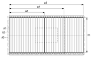
도 2는 본 개시의 일 실시예에 따른 디스플레이 패널부를 나타낸 정면도이다.
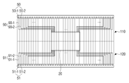
도 3은 본 개시의 일 실시예에 따른 디스플레이 모듈을 나타낸 확대도이다.
도 4는 도 3의 C-C 선을 따라 나타낸 단면도이다.
도 5는 본 개시의 일 실시 예에 따른 마이크로 LED, 구동 드라이버, 타이밍 컨트롤러 및 프로세서를 나타낸 블록도이다.
도 6a는 도 2의 A-A 선을 따라 나타낸 단면도이다.
도 6b는 도 2의 B-B 선을 따라 나타낸 단면도이다.
도 7a 및 도 7b는 복수의 디스플레이 모듈의 동작을 나타낸 일부의 디스플레이 모듈을 나타낸 확대도이다.
도 8은 복수의 디스플레이 모듈과 타이밍 컨트롤러의 연결을 나타낸 정면도이다.
도 9는 도 2의 다양한 디스플레이 영역을 나타낸 정면도이다.
도 10은 본 개시의 다른 실시예에 따른 디스플레이 패널부를 나타낸 정면도이다.
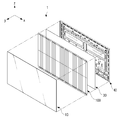
20: 타이밍 컨트롤러 30: 배열 플레이트
40: 하우징 50: 구동 드라이버
60: 인쇄회로기판 70: 연성회로기판
80: 프로세서 90: 전기적 경로
100: 디스플레이 패널부 110: 디스플레이 모듈
111: 박막 트랜지스터 기판 120: 추가 디스플레이 모듈
121: 추가 박막 트랜지스터 기판
130: 마이크로 LED
Claims (18)
- 인쇄회로기판; 및
상기 인쇄회로기판의 길이 방향을 따라 연속적으로 배치된 복수의 디스플레이 모듈;을 포함하고,
상기 복수의 디스플레이 모듈 각각은,
박막 트랜지스터 기판;
상기 박막 트랜지스터 기판의 일면에 배열된 복수의 마이크로 LED; 및
상기 인쇄회로기판과 상기 박막 트랜지스터 기판을 연결시키고, 일면에 상기 복수의 마이크로 LED를 제어하는 구동 드라이버가 배치된 연성회로기판(FPCB);을 포함하는 디스플레이 장치. - 제1항에 있어서,
상기 박막 트랜지스터 기판은, 제1 내지 제4 측면을 갖는 직사각형이며,
상기 제1 측면은 상기 연성회로기판과 인접하게 배치되며, 상기 제3 및 제4 측면은 제1 측면보다 긴 디스플레이 장치. - 제2항에 있어서,
상기 복수의 디스플레이 모듈 각각의 상기 제3 측면은 상호 평행하도록 배치된 디스플레이 장치. - 제3항에 있어서,
복수의 디스플레이 모듈 중, 하나의 디스플레이 모듈의 제3 측면은 상기 하나의 디스플레이 모듈과 인접한 다른 디스플레이 모듈의 제4 측면과 접촉하는 디스플레이 패널. - 제1항에 있어서,
상기 복수의 디스플레이 모듈 각각의 구동 드라이버에 영상 신호를 제공하는 타이밍 컨트롤러를 더 포함하는 디스플레이 장치. - 제5항에 있어서,
상기 타이밍 컨트롤러는 상기 복수의 디스플레이 모듈의 후방에 배치된 디스플레이 장치. - 제6항에 있어서,
상기 타이밍 컨트롤러는 상기 복수의 디스플레이 모듈의 중심에 배치된 디스플레이 장치. - 제7항에 있어서,
상기 타이밍 컨트롤러는 상기 타이밍 컨트롤러와 상기 복수의 디스플레이 모듈 각각의 상기 구동 드라이버의 거리의 합이 최소가 되도록 배치된 디스플레이 장치. - 제8항에 있어서,
상기 타이밍 컨트롤러는 상기 타이밍 컨트롤러를 중심으로 상기 복수의 디스플레이 모듈 각각의 상기 구동 드라이버가 대칭되도록 배치된 디스플레이 장치. - 제2항에 있어서,
상기 복수의 마이크로 LED는,
상기 제1 측면의 길이 방향을 따라 배열된 개수와 상기 제3 측면의 길이 방향을 따라 배열된 개수의 비가 1:9인 디스플레이 장치. - 제1항에 있어서,
상기 인쇄회로기판과 이격되어 평행하게 배치된 추가 인쇄회로기판; 및
상기 추가 인쇄회로기판의 길이 방향을 따라 연속적으로 배치된 복수의 추가 디스플레이 모듈;을 더 포함하는 디스플레이 장치. - 제11항에 있어서,
상기 복수의 디스플레이 모듈과 상기 복수의 추가 디스플레이 모듈은 서로 마주보도록 배치된 디스플레이 장치. - 제12항에 있어서,
상기 복수의 디스플레이 모듈 각각과 상기 복수의 추가 디스플레이 모듈 각각은 서로 마주보도록 배치된 디스플레이 장치. - 제13항에 있어서,
상기 복수의 디스플레이 모듈 각각과 상기 복수의 추가 디스플레이 모듈 각각은 서로 접촉하도록 배치된 디스플레이 장치. - 제13항에 있어서,
상기 복수의 디스플레이 모듈 각각과 상기 복수의 추가 디스플레이 모듈 각각은 일렬로 배치된 디스플레이 장치. - 제12항에 있어서,
상기 복수의 디스플레이 모듈의 가로 길이와 상기 복수의 디스플레이 모듈 및 상기 복수의 추가 디스플레이 모듈의 세로 길이의 비가 1:1, 16:9, 21:9 중 적어도 하나가 되도록 배치된 디스플레이 장치. - 제1항에 있어서,
상기 복수의 마이크로 LED는,
적색광을 방출하는 제1 마이크로 LED;
녹색광을 방출하는 제2 마이크로 LED; 및
청색광을 방출하는 제3 마이크로 LED;를 포함하고,
상기 제1 내지 제3 마이크로 LED는 하나의 픽셀을 구성하는 디스플레이 장치. - 제11항에 있어서,
상기 복수의 디스플레이 모듈 및 상기 복수의 추가 디스플레이 모듈이 동일 평면상에 평행하게 배치되도록 지지하는 배열 플레이트; 및
상기 복수의 디스플레이 모듈, 상기 복수의 추가 디스플레이 모듈 및 상기 배열 플레이트를 고정하는 하우징;을 더 포함하는 디스플레이 장치.
Priority Applications (6)
| Application Number | Priority Date | Filing Date | Title |
|---|---|---|---|
| KR1020180156304A KR20200069125A (ko) | 2018-12-06 | 2018-12-06 | 디스플레이 장치 |
| CN201980071674.1A CN112956022B (zh) | 2018-12-06 | 2019-11-29 | 显示装置 |
| EP19893409.3A EP3837717A4 (en) | 2018-12-06 | 2019-11-29 | DISPLAY DEVICE |
| PCT/KR2019/016649 WO2020116861A1 (en) | 2018-12-06 | 2019-11-29 | Display apparatus |
| US16/706,093 US10957245B2 (en) | 2018-12-06 | 2019-12-06 | Display apparatus having opposing display modules of micro LEDs |
| KR1020240166021A KR20240167423A (ko) | 2018-12-06 | 2024-11-20 | 디스플레이 장치 |
Applications Claiming Priority (1)
| Application Number | Priority Date | Filing Date | Title |
|---|---|---|---|
| KR1020180156304A KR20200069125A (ko) | 2018-12-06 | 2018-12-06 | 디스플레이 장치 |
Related Child Applications (1)
| Application Number | Title | Priority Date | Filing Date |
|---|---|---|---|
| KR1020240166021A Division KR20240167423A (ko) | 2018-12-06 | 2024-11-20 | 디스플레이 장치 |
Publications (1)
| Publication Number | Publication Date |
|---|---|
| KR20200069125A true KR20200069125A (ko) | 2020-06-16 |
Family
ID=70970736
Family Applications (2)
| Application Number | Title | Priority Date | Filing Date |
|---|---|---|---|
| KR1020180156304A Ceased KR20200069125A (ko) | 2018-12-06 | 2018-12-06 | 디스플레이 장치 |
| KR1020240166021A Pending KR20240167423A (ko) | 2018-12-06 | 2024-11-20 | 디스플레이 장치 |
Family Applications After (1)
| Application Number | Title | Priority Date | Filing Date |
|---|---|---|---|
| KR1020240166021A Pending KR20240167423A (ko) | 2018-12-06 | 2024-11-20 | 디스플레이 장치 |
Country Status (5)
| Country | Link |
|---|---|
| US (1) | US10957245B2 (ko) |
| EP (1) | EP3837717A4 (ko) |
| KR (2) | KR20200069125A (ko) |
| CN (1) | CN112956022B (ko) |
| WO (1) | WO2020116861A1 (ko) |
Families Citing this family (1)
| Publication number | Priority date | Publication date | Assignee | Title |
|---|---|---|---|---|
| CN115101531A (zh) * | 2021-03-05 | 2022-09-23 | 京东方科技集团股份有限公司 | 显示模组以及拼接显示装置 |
Family Cites Families (22)
| Publication number | Priority date | Publication date | Assignee | Title |
|---|---|---|---|---|
| JP2003149665A (ja) * | 2001-11-08 | 2003-05-21 | Hitachi Ltd | 液晶表示装置 |
| KR20020042589A (ko) | 2002-05-13 | 2002-06-05 | 강현인 | 벌집 구조의 도광판을 이용하여 이음매간 틈이 없는멀티비젼 구조를 만들어 이룩한 벽걸이형 박판 디스플레이 |
| JP3690378B2 (ja) * | 2002-07-26 | 2005-08-31 | 株式会社 日立ディスプレイズ | 表示装置 |
| US20070001927A1 (en) | 2005-07-01 | 2007-01-04 | Eastman Kodak Company | Tiled display for electronic signage |
| KR20070095029A (ko) * | 2006-03-20 | 2007-09-28 | 삼성전자주식회사 | 표시 장치 및 그의 제조 방법 |
| CN201017568Y (zh) * | 2007-06-22 | 2008-02-06 | 汪浩然 | 超薄柔性led显示屏系统 |
| KR100951274B1 (ko) * | 2007-07-19 | 2010-05-06 | 삼성엘이디 주식회사 | 백라이트 유닛 |
| US7905618B2 (en) | 2007-07-19 | 2011-03-15 | Samsung Led Co., Ltd. | Backlight unit |
| JP5254469B2 (ja) | 2009-12-03 | 2013-08-07 | シャープ株式会社 | 画像表示装置、パネルおよびパネルの製造方法 |
| WO2011071201A1 (ko) | 2009-12-11 | 2011-06-16 | (주)토비스 | 복수개의 엘시디 패널 연결에 의한 디스플레이 장치 |
| KR101350411B1 (ko) * | 2010-11-20 | 2014-01-16 | 엘지디스플레이 주식회사 | 멀티비젼용 어레이 기판 및 이를 구비한 액정표시장치 |
| WO2013094975A1 (en) * | 2011-12-23 | 2013-06-27 | Samsung Electronics Co., Ltd. | Display module and display apparatus having the same |
| KR102060788B1 (ko) * | 2012-12-31 | 2019-12-31 | 삼성디스플레이 주식회사 | 표시 장치 및 그 구동 방법 |
| KR102129336B1 (ko) | 2013-10-24 | 2020-07-03 | 삼성디스플레이 주식회사 | 표시 장치 및 멀티 패널 표시 장치 |
| KR102248841B1 (ko) | 2014-05-21 | 2021-05-06 | 삼성전자주식회사 | 디스플레이 장치, 전자 장치 및 전자 장치의 동작 방법 |
| WO2017146477A1 (ko) | 2016-02-26 | 2017-08-31 | 서울반도체주식회사 | 디스플레이 장치 및 그의 제조 방법 |
| KR102605174B1 (ko) | 2016-12-19 | 2023-11-22 | 엘지디스플레이 주식회사 | 발광 다이오드 디스플레이 장치 |
| KR102846822B1 (ko) * | 2016-12-27 | 2025-08-13 | 엘지디스플레이 주식회사 | 디스플레이용 회로 기판 모듈, 이를 포함하는 디스플레이 장치, 및 디스플레이용 회로 기판 모듈의 제조 방법 |
| KR102721847B1 (ko) | 2016-12-28 | 2024-10-25 | 엘지디스플레이 주식회사 | 멀티 디스플레이 시스템과 그 구동방법 |
| KR102565752B1 (ko) * | 2016-12-28 | 2023-08-11 | 엘지디스플레이 주식회사 | 전계 발광 표시장치와 그 구동 장치 |
| KR102687577B1 (ko) * | 2016-12-30 | 2024-07-22 | 엘지디스플레이 주식회사 | 발광 다이오드 표시 장치 및 이를 이용한 멀티 스크린 표시 장치 |
| KR102582059B1 (ko) * | 2016-12-30 | 2023-09-21 | 엘지디스플레이 주식회사 | 표시 장치 및 이를 이용한 멀티 스크린 표시 장치 |
-
2018
- 2018-12-06 KR KR1020180156304A patent/KR20200069125A/ko not_active Ceased
-
2019
- 2019-11-29 WO PCT/KR2019/016649 patent/WO2020116861A1/en not_active Ceased
- 2019-11-29 EP EP19893409.3A patent/EP3837717A4/en active Pending
- 2019-11-29 CN CN201980071674.1A patent/CN112956022B/zh active Active
- 2019-12-06 US US16/706,093 patent/US10957245B2/en active Active
-
2024
- 2024-11-20 KR KR1020240166021A patent/KR20240167423A/ko active Pending
Also Published As
| Publication number | Publication date |
|---|---|
| EP3837717A1 (en) | 2021-06-23 |
| US10957245B2 (en) | 2021-03-23 |
| KR20240167423A (ko) | 2024-11-26 |
| CN112956022A (zh) | 2021-06-11 |
| WO2020116861A1 (en) | 2020-06-11 |
| US20200184880A1 (en) | 2020-06-11 |
| EP3837717A4 (en) | 2021-10-20 |
| CN112956022B (zh) | 2025-02-25 |
Similar Documents
| Publication | Publication Date | Title |
|---|---|---|
| KR102558857B1 (ko) | 디스플레이 모듈 및 이를 이용한 대형 디스플레이 장치 | |
| KR102692864B1 (ko) | 발광 다이오드들을 갖는 백라이트 및 드라이버 집적 회로들이 활성 영역에 있는 전자 디바이스 디스플레이 | |
| US20220415873A1 (en) | Display module and display apparatus having the same | |
| TWI642979B (zh) | 背光裝置 | |
| CN101122716A (zh) | 背光组件和具有该背光组件的显示设备 | |
| CN107393415B (zh) | 一种显示面板和显示装置 | |
| CN109389910B (zh) | 微型发光二极管显示面板 | |
| JP5244181B2 (ja) | 照明装置、表示装置、及びテレビ受信装置 | |
| KR20220072535A (ko) | 디스플레이 모듈 | |
| US10771157B2 (en) | Mobile terminal and method for receiving and sending a LIFI signal thereof | |
| US20200219862A1 (en) | Display apparatus and method of manufacturing display apparatus thereof | |
| US11075329B2 (en) | Display panel with light emitting diode (LED) power transfer structure and display apparatus including the same | |
| KR20240167423A (ko) | 디스플레이 장치 | |
| KR20220072555A (ko) | 디스플레이 모듈 및 이를 포함하는 디스플레이 장치 | |
| KR102899916B1 (ko) | 디스플레이 모듈 및 디스플레이 장치 | |
| CN111103726A (zh) | 背光源、显示装置和背光源控制方法 | |
| JP5307766B2 (ja) | 電界放出装置 | |
| KR20210043997A (ko) | 디스플레이 장치 | |
| JP2023162080A (ja) | ディスプレイモジュールおよびディスプレイモジュールを含むディスプレイ装置 | |
| US12506131B2 (en) | Display module and display apparatus including the same | |
| EP3574374B1 (en) | Display panel, display control method, and display apparatus | |
| KR20220115297A (ko) | 디스플레이 장치 및 그 제어방법 | |
| KR20060095001A (ko) | 백 라이트의 구동장치와 이를 이용한 액정 표시장치 |
Legal Events
| Date | Code | Title | Description |
|---|---|---|---|
| PA0109 | Patent application |
St.27 status event code: A-0-1-A10-A12-nap-PA0109 |
|
| PG1501 | Laying open of application |
St.27 status event code: A-1-1-Q10-Q12-nap-PG1501 |
|
| A201 | Request for examination | ||
| PA0201 | Request for examination |
St.27 status event code: A-1-2-D10-D11-exm-PA0201 |
|
| D13-X000 | Search requested |
St.27 status event code: A-1-2-D10-D13-srh-X000 |
|
| D14-X000 | Search report completed |
St.27 status event code: A-1-2-D10-D14-srh-X000 |
|
| E902 | Notification of reason for refusal | ||
| PE0902 | Notice of grounds for rejection |
St.27 status event code: A-1-2-D10-D21-exm-PE0902 |
|
| E13-X000 | Pre-grant limitation requested |
St.27 status event code: A-2-3-E10-E13-lim-X000 |
|
| P11-X000 | Amendment of application requested |
St.27 status event code: A-2-2-P10-P11-nap-X000 |
|
| P13-X000 | Application amended |
St.27 status event code: A-2-2-P10-P13-nap-X000 |
|
| E601 | Decision to refuse application | ||
| PE0601 | Decision on rejection of patent |
St.27 status event code: N-2-6-B10-B15-exm-PE0601 |
|
| AMND | Amendment | ||
| E13-X000 | Pre-grant limitation requested |
St.27 status event code: A-2-3-E10-E13-lim-X000 |
|
| P11-X000 | Amendment of application requested |
St.27 status event code: A-2-2-P10-P11-nap-X000 |
|
| P13-X000 | Application amended |
St.27 status event code: A-2-2-P10-P13-nap-X000 |
|
| PX0901 | Re-examination |
St.27 status event code: A-2-3-E10-E12-rex-PX0901 |
|
| PX0601 | Decision of rejection after re-examination |
St.27 status event code: N-2-6-B10-B17-rex-PX0601 |
|
| X601 | Decision of rejection after re-examination | ||
| A107 | Divisional application of patent | ||
| PA0107 | Divisional application |
St.27 status event code: A-0-1-A10-A18-div-PA0107 St.27 status event code: A-0-1-A10-A16-div-PA0107 |
|
| P22-X000 | Classification modified |
St.27 status event code: A-2-2-P10-P22-nap-X000 |
|
| P22-X000 | Classification modified |
St.27 status event code: A-2-2-P10-P22-nap-X000 |