KR20200073099A - 반도체 회로 및 반도체 회로의 레이아웃 시스템 - Google Patents
반도체 회로 및 반도체 회로의 레이아웃 시스템 Download PDFInfo
- Publication number
- KR20200073099A KR20200073099A KR1020190024054A KR20190024054A KR20200073099A KR 20200073099 A KR20200073099 A KR 20200073099A KR 1020190024054 A KR1020190024054 A KR 1020190024054A KR 20190024054 A KR20190024054 A KR 20190024054A KR 20200073099 A KR20200073099 A KR 20200073099A
- Authority
- KR
- South Korea
- Prior art keywords
- node
- circuit
- inverter
- master latch
- clock signal
- Prior art date
- Legal status (The legal status is an assumption and is not a legal conclusion. Google has not performed a legal analysis and makes no representation as to the accuracy of the status listed.)
- Granted
Links
Images


Classifications
-
- G—PHYSICS
- G06—COMPUTING OR CALCULATING; COUNTING
- G06F—ELECTRIC DIGITAL DATA PROCESSING
- G06F30/00—Computer-aided design [CAD]
- G06F30/30—Circuit design
-
- G—PHYSICS
- G06—COMPUTING OR CALCULATING; COUNTING
- G06F—ELECTRIC DIGITAL DATA PROCESSING
- G06F1/00—Details not covered by groups G06F3/00 - G06F13/00 and G06F21/00
- G06F1/26—Power supply means, e.g. regulation thereof
- G06F1/32—Means for saving power
Landscapes
- Engineering & Computer Science (AREA)
- Theoretical Computer Science (AREA)
- Physics & Mathematics (AREA)
- General Engineering & Computer Science (AREA)
- General Physics & Mathematics (AREA)
- Computer Hardware Design (AREA)
- Semiconductor Integrated Circuits (AREA)
- Evolutionary Computation (AREA)
- Geometry (AREA)
- Design And Manufacture Of Integrated Circuits (AREA)
Abstract
Description
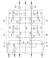
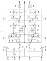
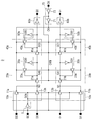
도 2 내지 도 5는 본 발명의 일 실시예에 따른 반도체 회로를 설명하기 위한 회로도이다.
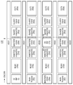
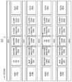
도 6 내지 도 9는 본 발명의 다양한 실시예에 따른 반도체 회로를 설명하기 위한 레이아웃도들이다.
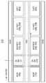
도 10 내지 도 12는 본 발명의 다양한 실시예에 따른 반도체 회로를 설명하기 위한 레이아웃도들이다.
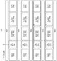
도 13 내지 도 16은 본 발명의 다양한 실시예에 따른 반도체 회로를 설명하기 위한 레이아웃도들이다.
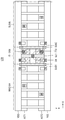
10a, 10b: 멀티플렉서 20a, 20b: 마스터 래치 주 회로
30a, 30b: 마스터 래치 보조 회로
40a, 40b: 슬레이브 래치 주 회로
50a, 50b: 슬레이브 래치 보조 회로
60a, 60b: 출력 드라이버 70: 클럭 인버터
100: 레이아웃 시스템 110: 프로세서
120: 메모리 130: 스토리지
140: 레이아웃 모듈 150: 입력 장치
160: 출력 장치
Claims (10)
- 클럭 신호를 반전시켜 반전 클럭 신호를 출력하는 클럭 인버터;
상기 클럭 신호 및 상기 반전 클럭 신호에 기초하여, 제1 노드 및 제4 노드의 신호를 각각 래치하여 제2 노드 및 제5 노드에 각각 전달하는 제1 마스터 래치 주 회로 및 제2 마스터 래치 주 회로;
상기 제2 노드 및 상기 제5 노드의 신호를 상기 제1 마스터 래치 주 회로 및 상기 제2 마스터 래치 주 회로에 각각 피드백하는 제1 마스터 래치 보조 회로 및 제2 마스터 래치 보조 회로;
상기 클럭 신호 및 상기 반전 클럭 신호에 기초하여, 상기 제2 노드 및 상기 제5 노드의 신호를 각각 래치하여 제3 노드 및 제6 노드에 각각 전달하는 제1 슬레이브 래치 주 회로 및 제2 슬레이브 래치 주 회로; 및
상기 제3 노드 및 상기 제6 노드의 신호를 상기 제1 슬레이브 래치 주 회로 및 상기 제2 슬레이브 래치 주 회로에 각각 피드백하는 제1 슬레이브 래치 보조 회로 및 제2 슬레이브 래치 보조 회로를 포함하고,
상기 클럭 인버터는 상기 제2 마스터 래치 주 회로와 상기 제2 슬레이브 래치 주 회로 사이에 배치되도록 레이아웃되는 반도체 회로. - 제1항에 있어서,
상기 제2 마스터 래치 주 회로는 상기 제2 마스터 래치 보조 회로와 상기 클럭 인버터 사이에 배치되도록 레이아웃되는 반도체 회로. - 제2항에 있어서,
상기 반도체 회로에 대한 스캔 동작을 위한 스캔 인에이블 신호를 반전시켜 반전 스캔 인에이블 신호를 출력하는 스캔 인에이블 인버터, 및
상기 스캔 인에이블 신호에 기초하여, 제1 비트 데이터 또는 제1 스캔 입력 신호를 선택하는 제1 멀티플렉서와 제2 비트 데이터 또는 제2 스캔 입력 신호를 선택하는 제2 멀티플렉서를 더 포함하고,
상기 클럭 인버터는 상기 스캔 인에이블 인버터와 다른 행에 배치되도록 레이아웃되는 반도체 회로. - 제3항에 있어서,
상기 클럭 인버터는 상기 스캔 인에이블 인버터와 다른 열에 배치되도록 레이아웃되는 반도체 회로. - 제3항에 있어서,
상기 제1 마스터 래치 주 회로는 상기 스캔 인에이블 인버터와 상기 제1 마스터 래치 보조 회로 사이에 배치되도록 레이아웃되는 반도체 회로. - 제3항에 있어서,
상기 제2 마스터 래치 보조 회로는 상기 스캔 인에이블 인버터와 동일한 열에 배치되도록 레이아웃되는 반도체 회로. - 스캔 동작을 위한 스캔 인에이블 신호를 반전시켜 반전 스캔 인에이블 신호를 출력하는 스캔 인에이블 인버터;
상기 스캔 인에이블 신호에 기초하여, 제1 비트 데이터 또는 제1 스캔 입력 신호를 선택하여 제1 노드에 출력하는 제1 멀티플렉서;
상기 스캔 인에이블 신호에 기초하여, 제2 비트 데이터 또는 제2 스캔 입력 신호를 선택하여 제4 노드에 출력하는 제2 멀티플렉서;
클럭 신호를 반전시켜 반전 클럭 신호를 출력하는 클럭 인버터;
상기 클럭 신호 및 상기 반전 클럭 신호에 기초하여, 상기 제1 노드 및 상기 제4 노드의 신호를 각각 래치하여 제2 노드 및 제5 노드에 각각 전달하는 제1 마스터 래치 회로 및 제2 마스터 래치 회로; 및
상기 클럭 신호 및 상기 반전 클럭 신호에 기초하여, 상기 제2 노드 및 상기 제5 노드의 신호를 각각 래치하여 제3 노드 및 제6 노드에 각각 전달하는 제1 슬레이브 래치 회로 및 제2 슬레이브 래치 회로를 포함하고,
상기 클럭 인버터는 상기 제2 멀티플렉서와 상기 제2 마스터 래치 회로 사이에 배치되도록 레이아웃되는 반도체 회로. - 제7항에 있어서,
상기 스캔 인에이블 인버터는 상기 제1 멀티플렉서와 상기 제1 마스터 래치 회로 사이에 배치되도록 레이아웃되는 반도체 회로. - 제7항에 있어서,
상기 클럭 인버터는 상기 스캔 인에이블 인버터와 다른 행에 배치되도록 레이아웃되는 반도체 회로. - 제9항에 있어서,
상기 클럭 인버터는 상기 스캔 인에이블 인버터와 동일한 열에 배치되도록 레이아웃되는 반도체 회로.
Priority Applications (2)
| Application Number | Priority Date | Filing Date | Title |
|---|---|---|---|
| US16/535,611 US10868524B2 (en) | 2018-12-13 | 2019-08-08 | Semiconductor circuit and semiconductor circuit layout system |
| TW108145274A TWI812821B (zh) | 2018-12-13 | 2019-12-11 | 半導體電路及半導體電路佈局系統 |
Applications Claiming Priority (2)
| Application Number | Priority Date | Filing Date | Title |
|---|---|---|---|
| KR20180161016 | 2018-12-13 | ||
| KR1020180161016 | 2018-12-13 |
Publications (2)
| Publication Number | Publication Date |
|---|---|
| KR20200073099A true KR20200073099A (ko) | 2020-06-23 |
| KR102627943B1 KR102627943B1 (ko) | 2024-01-22 |
Family
ID=71138229
Family Applications (1)
| Application Number | Title | Priority Date | Filing Date |
|---|---|---|---|
| KR1020190024054A Active KR102627943B1 (ko) | 2018-12-13 | 2019-02-28 | 반도체 회로 및 반도체 회로의 레이아웃 시스템 |
Country Status (2)
| Country | Link |
|---|---|
| KR (1) | KR102627943B1 (ko) |
| TW (1) | TWI812821B (ko) |
Families Citing this family (1)
| Publication number | Priority date | Publication date | Assignee | Title |
|---|---|---|---|---|
| KR20230136262A (ko) * | 2022-03-18 | 2023-09-26 | 삼성전자주식회사 | 레이아웃 설계 장치 |
Citations (4)
| Publication number | Priority date | Publication date | Assignee | Title |
|---|---|---|---|---|
| US8717078B2 (en) * | 2012-06-13 | 2014-05-06 | Arm Limited | Sequential latching device with elements to increase hold times on the diagnostic data path |
| US8819508B2 (en) * | 2012-10-05 | 2014-08-26 | Lsi Corporation | Scan test circuitry configured to prevent violation of multiplexer select signal constraints during scan testing |
| US9424124B2 (en) * | 2012-06-14 | 2016-08-23 | Infineon Technologies Ag | Error-tolerant memories |
| US9742383B2 (en) * | 2015-09-11 | 2017-08-22 | Kabushiki Kaisha Toshiba | Semiconductor integrated circuit |
Family Cites Families (5)
| Publication number | Priority date | Publication date | Assignee | Title |
|---|---|---|---|---|
| US8456214B2 (en) * | 2009-11-17 | 2013-06-04 | Arm Limited | State retention circuit and method of operation of such a circuit |
| US8493120B2 (en) * | 2011-03-10 | 2013-07-23 | Arm Limited | Storage circuitry and method with increased resilience to single event upsets |
| TWI475368B (zh) * | 2012-11-21 | 2015-03-01 | Giga Byte Tech Co Ltd | 電源控制系統及其方法 |
| CN107408939B (zh) * | 2015-04-01 | 2020-09-25 | 国立研究开发法人科学技术振兴机构 | 电子电路 |
| TWI537964B (zh) * | 2015-04-20 | 2016-06-11 | 華邦電子股份有限公司 | 反及閘快閃記憶體和其操作方法 |
-
2019
- 2019-02-28 KR KR1020190024054A patent/KR102627943B1/ko active Active
- 2019-12-11 TW TW108145274A patent/TWI812821B/zh active
Patent Citations (4)
| Publication number | Priority date | Publication date | Assignee | Title |
|---|---|---|---|---|
| US8717078B2 (en) * | 2012-06-13 | 2014-05-06 | Arm Limited | Sequential latching device with elements to increase hold times on the diagnostic data path |
| US9424124B2 (en) * | 2012-06-14 | 2016-08-23 | Infineon Technologies Ag | Error-tolerant memories |
| US8819508B2 (en) * | 2012-10-05 | 2014-08-26 | Lsi Corporation | Scan test circuitry configured to prevent violation of multiplexer select signal constraints during scan testing |
| US9742383B2 (en) * | 2015-09-11 | 2017-08-22 | Kabushiki Kaisha Toshiba | Semiconductor integrated circuit |
Also Published As
| Publication number | Publication date |
|---|---|
| TWI812821B (zh) | 2023-08-21 |
| KR102627943B1 (ko) | 2024-01-22 |
| TW202036359A (zh) | 2020-10-01 |
Similar Documents
| Publication | Publication Date | Title |
|---|---|---|
| US12063041B2 (en) | Flip flop standard cell | |
| CN101859600B (zh) | 集成电路结构 | |
| CN106533395B (zh) | 半导体集成电路和触发器 | |
| US9805790B2 (en) | Memory cell with retention using resistive memory | |
| US10868524B2 (en) | Semiconductor circuit and semiconductor circuit layout system | |
| US10673420B2 (en) | Electronic circuit including flip-flop using common clock | |
| TWI811500B (zh) | 半導體電路 | |
| CN115395925A (zh) | 包括触发器的集成电路和用于设计集成电路的计算系统 | |
| US11386254B2 (en) | Semiconductor circuit and semiconductor circuit layout system | |
| KR102627943B1 (ko) | 반도체 회로 및 반도체 회로의 레이아웃 시스템 | |
| US8181073B2 (en) | SRAM macro test flop | |
| US11988712B2 (en) | Multi-bit flip-flop and integrated circuit including the same | |
| US11394374B2 (en) | Semiconductor device | |
| CN110689911A (zh) | 半导体存储器设备 | |
| KR20240004607A (ko) | 기록 마스크드 래치 비트 셀 | |
| KR20240004963A (ko) | 하이브리드 라이브러리 래치 어레이 | |
| US6800882B2 (en) | Multiple-bit memory latch cell for integrated circuit gate array | |
| US8717795B2 (en) | Semiconductor device having plural circuit blocks operating at the same timing | |
| KR20210085652A (ko) | 반도체 장치의 퓨즈 래치 | |
| KR19990038259A (ko) | 메모리 셀 버퍼 |
Legal Events
| Date | Code | Title | Description |
|---|---|---|---|
| PA0109 | Patent application |
Patent event code: PA01091R01D Comment text: Patent Application Patent event date: 20190228 |
|
| PG1501 | Laying open of application | ||
| A201 | Request for examination | ||
| PA0201 | Request for examination |
Patent event code: PA02012R01D Patent event date: 20220117 Comment text: Request for Examination of Application Patent event code: PA02011R01I Patent event date: 20190228 Comment text: Patent Application |
|
| E701 | Decision to grant or registration of patent right | ||
| PE0701 | Decision of registration |
Patent event code: PE07011S01D Comment text: Decision to Grant Registration Patent event date: 20231130 |
|
| GRNT | Written decision to grant | ||
| PR0701 | Registration of establishment |
Comment text: Registration of Establishment Patent event date: 20240117 Patent event code: PR07011E01D |
|
| PR1002 | Payment of registration fee |
Payment date: 20240117 End annual number: 3 Start annual number: 1 |
|
| PG1601 | Publication of registration |