KR20200073592A - 메모리 컨트롤러 및 이를 포함하는 메모리 시스템 - Google Patents
메모리 컨트롤러 및 이를 포함하는 메모리 시스템 Download PDFInfo
- Publication number
- KR20200073592A KR20200073592A KR1020180161926A KR20180161926A KR20200073592A KR 20200073592 A KR20200073592 A KR 20200073592A KR 1020180161926 A KR1020180161926 A KR 1020180161926A KR 20180161926 A KR20180161926 A KR 20180161926A KR 20200073592 A KR20200073592 A KR 20200073592A
- Authority
- KR
- South Korea
- Prior art keywords
- memory
- memory system
- size
- throughput
- memory controller
- Prior art date
- Legal status (The legal status is an assumption and is not a legal conclusion. Google has not performed a legal analysis and makes no representation as to the accuracy of the status listed.)
- Granted
Links
Images




Classifications
-
- G—PHYSICS
- G06—COMPUTING OR CALCULATING; COUNTING
- G06F—ELECTRIC DIGITAL DATA PROCESSING
- G06F13/00—Interconnection of, or transfer of information or other signals between, memories, input/output devices or central processing units
- G06F13/14—Handling requests for interconnection or transfer
- G06F13/16—Handling requests for interconnection or transfer for access to memory bus
- G06F13/1668—Details of memory controller
- G06F13/1689—Synchronisation and timing concerns
-
- G—PHYSICS
- G06—COMPUTING OR CALCULATING; COUNTING
- G06F—ELECTRIC DIGITAL DATA PROCESSING
- G06F3/00—Input arrangements for transferring data to be processed into a form capable of being handled by the computer; Output arrangements for transferring data from processing unit to output unit, e.g. interface arrangements
- G06F3/06—Digital input from, or digital output to, record carriers, e.g. RAID, emulated record carriers or networked record carriers
- G06F3/0601—Interfaces specially adapted for storage systems
- G06F3/0628—Interfaces specially adapted for storage systems making use of a particular technique
- G06F3/0655—Vertical data movement, i.e. input-output transfer; data movement between one or more hosts and one or more storage devices
- G06F3/0658—Controller construction arrangements
-
- G—PHYSICS
- G06—COMPUTING OR CALCULATING; COUNTING
- G06F—ELECTRIC DIGITAL DATA PROCESSING
- G06F12/00—Accessing, addressing or allocating within memory systems or architectures
- G06F12/02—Addressing or allocation; Relocation
- G06F12/0223—User address space allocation, e.g. contiguous or non contiguous base addressing
- G06F12/023—Free address space management
- G06F12/0238—Memory management in non-volatile memory, e.g. resistive RAM or ferroelectric memory
- G06F12/0246—Memory management in non-volatile memory, e.g. resistive RAM or ferroelectric memory in block erasable memory, e.g. flash memory
-
- G—PHYSICS
- G06—COMPUTING OR CALCULATING; COUNTING
- G06F—ELECTRIC DIGITAL DATA PROCESSING
- G06F12/00—Accessing, addressing or allocating within memory systems or architectures
- G06F12/02—Addressing or allocation; Relocation
- G06F12/0223—User address space allocation, e.g. contiguous or non contiguous base addressing
- G06F12/023—Free address space management
- G06F12/0253—Garbage collection, i.e. reclamation of unreferenced memory
-
- G—PHYSICS
- G06—COMPUTING OR CALCULATING; COUNTING
- G06F—ELECTRIC DIGITAL DATA PROCESSING
- G06F3/00—Input arrangements for transferring data to be processed into a form capable of being handled by the computer; Output arrangements for transferring data from processing unit to output unit, e.g. interface arrangements
- G06F3/06—Digital input from, or digital output to, record carriers, e.g. RAID, emulated record carriers or networked record carriers
- G06F3/0601—Interfaces specially adapted for storage systems
- G06F3/0602—Interfaces specially adapted for storage systems specifically adapted to achieve a particular effect
- G06F3/0604—Improving or facilitating administration, e.g. storage management
-
- G—PHYSICS
- G06—COMPUTING OR CALCULATING; COUNTING
- G06F—ELECTRIC DIGITAL DATA PROCESSING
- G06F3/00—Input arrangements for transferring data to be processed into a form capable of being handled by the computer; Output arrangements for transferring data from processing unit to output unit, e.g. interface arrangements
- G06F3/06—Digital input from, or digital output to, record carriers, e.g. RAID, emulated record carriers or networked record carriers
- G06F3/0601—Interfaces specially adapted for storage systems
- G06F3/0602—Interfaces specially adapted for storage systems specifically adapted to achieve a particular effect
- G06F3/061—Improving I/O performance
- G06F3/0613—Improving I/O performance in relation to throughput
-
- G—PHYSICS
- G06—COMPUTING OR CALCULATING; COUNTING
- G06F—ELECTRIC DIGITAL DATA PROCESSING
- G06F3/00—Input arrangements for transferring data to be processed into a form capable of being handled by the computer; Output arrangements for transferring data from processing unit to output unit, e.g. interface arrangements
- G06F3/06—Digital input from, or digital output to, record carriers, e.g. RAID, emulated record carriers or networked record carriers
- G06F3/0601—Interfaces specially adapted for storage systems
- G06F3/0628—Interfaces specially adapted for storage systems making use of a particular technique
- G06F3/0638—Organizing or formatting or addressing of data
- G06F3/064—Management of blocks
-
- G—PHYSICS
- G06—COMPUTING OR CALCULATING; COUNTING
- G06F—ELECTRIC DIGITAL DATA PROCESSING
- G06F3/00—Input arrangements for transferring data to be processed into a form capable of being handled by the computer; Output arrangements for transferring data from processing unit to output unit, e.g. interface arrangements
- G06F3/06—Digital input from, or digital output to, record carriers, e.g. RAID, emulated record carriers or networked record carriers
- G06F3/0601—Interfaces specially adapted for storage systems
- G06F3/0628—Interfaces specially adapted for storage systems making use of a particular technique
- G06F3/0655—Vertical data movement, i.e. input-output transfer; data movement between one or more hosts and one or more storage devices
-
- G—PHYSICS
- G06—COMPUTING OR CALCULATING; COUNTING
- G06F—ELECTRIC DIGITAL DATA PROCESSING
- G06F3/00—Input arrangements for transferring data to be processed into a form capable of being handled by the computer; Output arrangements for transferring data from processing unit to output unit, e.g. interface arrangements
- G06F3/06—Digital input from, or digital output to, record carriers, e.g. RAID, emulated record carriers or networked record carriers
- G06F3/0601—Interfaces specially adapted for storage systems
- G06F3/0628—Interfaces specially adapted for storage systems making use of a particular technique
- G06F3/0655—Vertical data movement, i.e. input-output transfer; data movement between one or more hosts and one or more storage devices
- G06F3/0656—Data buffering arrangements
-
- G—PHYSICS
- G06—COMPUTING OR CALCULATING; COUNTING
- G06F—ELECTRIC DIGITAL DATA PROCESSING
- G06F3/00—Input arrangements for transferring data to be processed into a form capable of being handled by the computer; Output arrangements for transferring data from processing unit to output unit, e.g. interface arrangements
- G06F3/06—Digital input from, or digital output to, record carriers, e.g. RAID, emulated record carriers or networked record carriers
- G06F3/0601—Interfaces specially adapted for storage systems
- G06F3/0628—Interfaces specially adapted for storage systems making use of a particular technique
- G06F3/0655—Vertical data movement, i.e. input-output transfer; data movement between one or more hosts and one or more storage devices
- G06F3/0659—Command handling arrangements, e.g. command buffers, queues, command scheduling
-
- G—PHYSICS
- G06—COMPUTING OR CALCULATING; COUNTING
- G06F—ELECTRIC DIGITAL DATA PROCESSING
- G06F3/00—Input arrangements for transferring data to be processed into a form capable of being handled by the computer; Output arrangements for transferring data from processing unit to output unit, e.g. interface arrangements
- G06F3/06—Digital input from, or digital output to, record carriers, e.g. RAID, emulated record carriers or networked record carriers
- G06F3/0601—Interfaces specially adapted for storage systems
- G06F3/0668—Interfaces specially adapted for storage systems adopting a particular infrastructure
- G06F3/0671—In-line storage system
- G06F3/0673—Single storage device
-
- G—PHYSICS
- G06—COMPUTING OR CALCULATING; COUNTING
- G06F—ELECTRIC DIGITAL DATA PROCESSING
- G06F3/00—Input arrangements for transferring data to be processed into a form capable of being handled by the computer; Output arrangements for transferring data from processing unit to output unit, e.g. interface arrangements
- G06F3/06—Digital input from, or digital output to, record carriers, e.g. RAID, emulated record carriers or networked record carriers
- G06F3/0601—Interfaces specially adapted for storage systems
- G06F3/0668—Interfaces specially adapted for storage systems adopting a particular infrastructure
- G06F3/0671—In-line storage system
- G06F3/0673—Single storage device
- G06F3/0679—Non-volatile semiconductor memory device, e.g. flash memory, one time programmable memory [OTP]
Landscapes
- Engineering & Computer Science (AREA)
- Theoretical Computer Science (AREA)
- Physics & Mathematics (AREA)
- General Engineering & Computer Science (AREA)
- General Physics & Mathematics (AREA)
- Human Computer Interaction (AREA)
- Memory System (AREA)
- Memory System Of A Hierarchy Structure (AREA)
- Dram (AREA)
Abstract
Description
도 2는 본 발명의 실시예에 따른 메모리 컨트롤러를 설명하기 위한 도면이다.
도 3은 도 2의 중앙 처리 장치를 설명하기 위한 도면이다.
도 4는 본 발명의 다른 실시예에 따른 메모리 컨트롤러를 설명하기 위한 도면이다.
도 5는 도 4의 중앙 처리 장치를 설명하기 위한 도면이다.
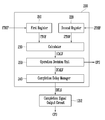
도 6은 본 발명의 실시예에 따른 스로틀링 매니저를 설명하기 위한 도면이다.
도 7은 본 발명의 실시예에 따른 메모리 시스템의 동작을 설명하기 위한 순서도이다.
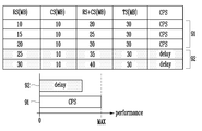
도 8은 요청 처리량 사이즈와 현재 처리량 사이즈에 영향을 주는 요소들(elements)의 실시예를 설명하기 위한 표 이다.
도 9는 본 발명의 실시예에 따라 완료 신호(completion signal)가 출력 또는 지연되는 다양한 경우들을 설명하기 위한 도면이다.
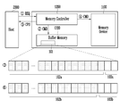
도 10은 커맨드들이 저장되는 버퍼 메모리에 관계 없이, 내부 처리량에 따라 완료 신호(completion signal)를 출력하는 메모리 시스템의 동작을 설명하기 위한 도면이다.
도 11은 본 발명의 다른 실시예에 따른 스로틀링 매니저를 설명하기 위한 도면이다.
도 12 내지 도 16은 본 발명의 또 다른 실시예를 설명하기 위한 도면이다.
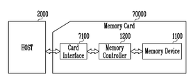
도 17은 도 1에 도시된 메모리 시스템의 다른 실시 예를 설명하기 위한 도면이다.
도 18은 도 1에 도시된 메모리 시스템의 다른 실시 예를 설명하기 위한 도면이다.
도 19는 도 1에 도시된 메모리 시스템의 다른 실시 예를 설명하기 위한 도면이다.
도 20은 도 1에 도시된 메모리 시스템의 다른 실시 예를 설명하기 위한 도면이다.
1200: 메모리 컨트롤러 1300: 버퍼 메모리
2000: 호스트 1211: 커맨드 생성부
1212: 완료 신호 출력 모듈 200: 스로틀링 매니저
210: 제1 레지스터 220: 제2 레지스터
230: 연산기 240: 완료 지연 매니저
Claims (19)
- 호스트로부터 수신받은 요청에 따라 커맨드를 생성하는 커맨드 생성부;
메모리 시스템의 내부에서 현재 처리중인 데이터의 현재 처리량 사이즈와 앞으로 처리할 데이터의 요청 처리량 사이즈를 비교하여 지연 신호를 활성화 또는 비활성화시키는 스로틀링 매니저; 및
상기 지연 신호가 활성화되는 동안, 상기 요청에 대한 완료 신호의 출력을 지연시키고, 상기 지연 신호가 비활성화되면 상기 완료 신호를 출력하는 완료 신호 출력 모듈을 포함하는 메모리 컨트롤러.
- 제1항에 있어서, 상기 커맨드 생성부는,
상기 요청을 상기 메모리 시스템의 내부에서 사용될 수 있는 상기 커맨드로 변환하는 메모리 컨트롤러.
- 제1항에 있어서, 상기 스로틀링 매니저는,
상기 현재 처리량 사이즈의 정보를 임시로 저장하는 제1 레지스터;
상기 요청 처리량 사이즈의 정보를 임시로 저장하는 제2 레지스터;
상기 제1 및 제2 레지스터들로부터 상기 현재 처리량 사이즈와 상기 요청 처리량 사이즈를 연산하여 제1 연산값을 출력하는 연산기; 및
상기 제1 연산값에 따라 상기 지연 신호를 활성화 또는 비활성화하는 완료 지연 매니저를 포함하는 메모리 컨트롤러.
- 제3항에 있어서, 상기 연산기는,
상기 현재 처리량 사이즈와 상기 요청 처리량 사이즈를 합하여 총 처리량 사이즈를 산출하고,
상기 총 처리량 사이즈를 목표 사이즈와 비교하고, 비교 결과에 따라 상기 제1 연산값을 출력하는 메모리 컨트롤러.
- 제4항에 있어서, 상기 목표 사이즈는,
상기 메모리 시스템에서 스로틀링 동작이 수행되는 기준 값인 메모리 컨트롤러.
- 제4항에 있어서, 상기 완료 지연 매니저는,
상기 총 처리량이 상기 목표 사이즈보다 크면, 상기 제1 연산값에 따라 상기 완료 신호를 지연시키기 위한 상기 지연 신호를 활성화시키고,
상기 총 처리량이 상기 목표 사이즈보다 작으면, 상기 제1 연산값에 따라 상기 지연 신호를 비활성화시키는 메모리 컨트롤러.
- 제1항에 있어서,
상기 현재 처리량 사이즈는 상기 메모리 시스템의 내부에서 처리되고 있는 현재 데이터 사이즈이거나, 상기 메모리 시스템의 내부에서 실행중인 커맨드들의 개수이거나, 상기 메모리 시스템의 내부에 큐잉된 커맨드들의 깊이(depth) 중 적어도 하나 이상을 포함하는 메모리 컨트롤러.
- 제1항에 있어서,
상기 요청 처리량 사이즈는 상기 호스트에 의해 요청된 데이터 사이즈이거나, 상기 호스트에 의해 요청된 커맨드들의 개수이거나, 상기 호스트에 의해 요청된 커맨드들의 깊이 중 적어도 하나 이상을 포함하는 메모리 컨트롤러.
- 제3항에 있어서,
상기 제1 연산값에 따라 상기 메모리 시스템의 백그라운드 동작을 실행하기 위한 동작 신호를 출력하는 동작 결정부를 더 포함하는 메모리 컨트롤러.
- 제9항에 있어서, 상기 동작 결정부는,
상기 제1 연산값을 토대로 하여 상기 메모리 시스템의 내부에서 처리되는 데이터 사이즈가 기준값보다 많은 것으로 판단되면 상기 동작 신호를 비활성화하고,
상기 제1 연산값을 토대로 하여 상기 메모리 시스템의 내부에서 처리되는 데이터 사이즈가 상기 기준값보다 적거나 같은 것으로 판단되면 상기 동작 신호를 활성화하는 메모리 컨트롤러.
- 제10항에 있어서,
상기 기준값은 가비지 컬렉션 동작 또는 웨어 레벨링 동작이 수행되는 기준값인 메모리 컨트롤러.
- 제11항에 있어서,
상기 동작 신호가 출력되면, 상기 커맨드 생성부는 상기 가비지 컬렉션 동작 또는 상기 웨어 레벨링 동작을 수행하기 위한 커맨드들을 생성하는 메모리 컨트롤러.
- 제9항에 있어서,
상기 동작 결정부는 상기 동작 신호를 출력할 때, 상기 제1 연산값과 동일한 제2 연산값을 상기 완료 지연 매니저에게 출력하는 메모리 컨트롤러.
- 데이터가 저장되는 다수의 다이들(dies);
호스트와 상기 다이들 사이에서 통신하는 메모리 컨트롤러; 및
상기 메모리 컨트롤러에서 생성된 커맨드들을 임시로 저장하는 버퍼 메모리를 포함하고,
상기 메모리 컨트롤러는,
상기 다이들에 포함된 다수의 메모리 블록들을 다수의 슈퍼 블록들로 그룹화하고, 상기 슈퍼 블록들 각각의 현재 처리량 사이즈와 앞으로 처리할 요청 처리량 사이즈에 따라 스로틀링 비율을 조절하고, 상기 스로틀링 비율에 따라 상기 슈퍼 블록들의 성능 값을 각각 조절하는 메모리 시스템.
- 제14항에 있어서, 상기 메모리 컨트롤러는,
상기 슈퍼 블록들 중 상기 스로틀링 비율이 상대적으로 낮은 슈퍼 블록들의 성능 값을 높이고,
상기 슈퍼 블록들 중 상기 스로틀링 비율이 상대적으로 높은 슈퍼 블록들의 성능 값을 낮추는 메모리 시스템.
- 제15항에 있어서,
상기 스로틀링 비율은 메모리 시스템의 평균 성능 값에서 상기 슈퍼 블록의 성능 값을 빼어 산출되는 메모리 시스템.
- 제16항에 있어서,
상기 평균 성능 값은 상기 슈퍼 블록들 각각의 성능 값들을 상기 슈퍼 블록들의 개수로 나누어 산출되는 메모리 시스템.
- 제17항에 있어서,
상기 슈퍼 블록들 각각의 상기 성능 값들은 상기 메모리 시스템의 최대 성능 값을 지표로 나누어 산출되는 메모리 시스템.
- 제18항에 있어서,
상기 지표는 상기 슈퍼 블록들 각각의 상기 현재 처리량 사이즈를 상기 요청 처리량 사이즈로 나누어 산출되는 메모리 시스템.
Priority Applications (3)
| Application Number | Priority Date | Filing Date | Title |
|---|---|---|---|
| KR1020180161926A KR102669517B1 (ko) | 2018-12-14 | 2018-12-14 | 메모리 컨트롤러 및 이를 포함하는 메모리 시스템 |
| US16/533,050 US11086528B2 (en) | 2018-12-14 | 2019-08-06 | Memory controller and memory system having the same |
| CN201910930006.1A CN111324301B (zh) | 2018-12-14 | 2019-09-29 | 存储器控制器以及具有存储器控制器的存储器系统 |
Applications Claiming Priority (1)
| Application Number | Priority Date | Filing Date | Title |
|---|---|---|---|
| KR1020180161926A KR102669517B1 (ko) | 2018-12-14 | 2018-12-14 | 메모리 컨트롤러 및 이를 포함하는 메모리 시스템 |
Publications (2)
| Publication Number | Publication Date |
|---|---|
| KR20200073592A true KR20200073592A (ko) | 2020-06-24 |
| KR102669517B1 KR102669517B1 (ko) | 2024-05-29 |
Family
ID=71073700
Family Applications (1)
| Application Number | Title | Priority Date | Filing Date |
|---|---|---|---|
| KR1020180161926A Active KR102669517B1 (ko) | 2018-12-14 | 2018-12-14 | 메모리 컨트롤러 및 이를 포함하는 메모리 시스템 |
Country Status (3)
| Country | Link |
|---|---|
| US (1) | US11086528B2 (ko) |
| KR (1) | KR102669517B1 (ko) |
| CN (1) | CN111324301B (ko) |
Cited By (5)
| Publication number | Priority date | Publication date | Assignee | Title |
|---|---|---|---|---|
| KR20220130518A (ko) * | 2021-03-18 | 2022-09-27 | 에스케이하이닉스 주식회사 | PCIe 디바이스 및 그 동작 방법 |
| US11841819B2 (en) | 2021-03-23 | 2023-12-12 | SK Hynix Inc. | Peripheral component interconnect express interface device and method of operating the same |
| US11922062B2 (en) | 2021-03-10 | 2024-03-05 | SK Hynix Inc. | Controller and operating method thereof |
| US12007918B2 (en) | 2021-03-23 | 2024-06-11 | SK Hynix Inc. | Peripheral component interconnect express interface device and method of operating the same |
| US12216599B2 (en) | 2021-03-18 | 2025-02-04 | SK Hynix Inc. | Peripheral component interconnect express (PCIe) device method for delaying command operations based on generated throughput analysis information |
Families Citing this family (2)
| Publication number | Priority date | Publication date | Assignee | Title |
|---|---|---|---|---|
| US11093244B2 (en) * | 2019-08-28 | 2021-08-17 | Micron Technology, Inc. | Command delay |
| US11321017B2 (en) * | 2020-06-29 | 2022-05-03 | SK Hynix Inc. | Systems and methods for controlling completion rate of commands |
Citations (4)
| Publication number | Priority date | Publication date | Assignee | Title |
|---|---|---|---|---|
| JP2014010476A (ja) * | 2012-06-27 | 2014-01-20 | Fujitsu Ltd | ストレージ仮想化装置、ストレージ仮想化方法及びストレージ仮想化プログラム |
| KR20170085286A (ko) * | 2016-01-14 | 2017-07-24 | 에스케이하이닉스 주식회사 | 메모리 시스템 및 메모리 시스템의 동작 방법 |
| KR20180026876A (ko) * | 2016-09-05 | 2018-03-14 | 에스케이하이닉스 주식회사 | 메모리 시스템 및 메모리 시스템의 동작방법 |
| KR20180113861A (ko) * | 2017-04-07 | 2018-10-17 | 삼성전자주식회사 | 트래픽 제어 방법 및 그 전자 장치 |
Family Cites Families (25)
| Publication number | Priority date | Publication date | Assignee | Title |
|---|---|---|---|---|
| US6968409B1 (en) * | 2001-08-29 | 2005-11-22 | Lsi Logic Corporation | Method and apparatus of establishing a dynamically adjustable loop of delayed read commands for completion in a queue buffer |
| US8015281B2 (en) * | 2008-04-21 | 2011-09-06 | Microsoft Corporation | Dynamic server flow control in a hybrid peer-to-peer network |
| US7853681B2 (en) * | 2008-06-30 | 2010-12-14 | International Business Machines Corporation | Method for controlling host throughput to a computer storage subsystem |
| US8656088B2 (en) * | 2011-05-20 | 2014-02-18 | International Business Machines Corporation | Optimized flash based cache memory |
| KR101861184B1 (ko) * | 2011-11-02 | 2018-05-28 | 삼성전자주식회사 | 스토리지의 동작 성능 조절방법 및 그에 따른 반도체 저장장치 |
| US9130969B2 (en) * | 2012-08-23 | 2015-09-08 | Seagate Technology Llc | Data storage I/O communication method and apparatus |
| US9575677B2 (en) * | 2014-04-29 | 2017-02-21 | Sandisk Technologies Llc | Storage system power management using controlled execution of pending memory commands |
| US9093160B1 (en) | 2014-05-30 | 2015-07-28 | Sandisk Technologies Inc. | Methods and systems for staggered memory operations |
| KR102317786B1 (ko) | 2015-02-02 | 2021-10-26 | 삼성전자주식회사 | 스토리지 디바이스에서의 입출력 처리 방법 및 이를 적용하는 스토리지 디바이스 및 비휘발성 메모리 디바이스 |
| KR102076196B1 (ko) | 2015-04-14 | 2020-02-12 | 에스케이하이닉스 주식회사 | 메모리 시스템, 메모리 모듈 및 메모리 모듈의 동작 방법 |
| US9778878B2 (en) * | 2015-04-22 | 2017-10-03 | Sandisk Technologies Llc | Method and system for limiting write command execution |
| US20170212711A1 (en) | 2016-01-21 | 2017-07-27 | Kabushiki Kaisha Toshiba | Disk apparatus and control method |
| US10313251B2 (en) * | 2016-02-01 | 2019-06-04 | Netapp, Inc. | Methods and systems for managing quality of service in a networked storage environment |
| CN107526532B (zh) * | 2016-06-21 | 2020-07-10 | 伊姆西Ip控股有限责任公司 | 调节存储设备的吞吐量的方法和装置 |
| US10007311B2 (en) * | 2016-08-15 | 2018-06-26 | Sandisk Technologies Llc | Adaptive temperature and memory parameter throttling |
| US10956083B2 (en) * | 2016-12-16 | 2021-03-23 | Western Digital Technologies, Inc. | Method and system for input-output throttling to improve quality of service in a solid state drive |
| US10140027B1 (en) * | 2017-05-26 | 2018-11-27 | Seagate Technology Llc | Data transfers with adaptively adjusted polling times |
| US10013194B1 (en) * | 2017-06-02 | 2018-07-03 | Western Digital Technologies, Inc. | Handling thermal shutdown for memory devices |
| US10824363B2 (en) * | 2017-07-07 | 2020-11-03 | Dell Products, L.P. | System and method of characterization of a system having persistent memory |
| US10198353B2 (en) * | 2017-07-07 | 2019-02-05 | Dell Products, Lp | Device and method for implementing save operation of persistent memory |
| US10514748B2 (en) * | 2017-09-27 | 2019-12-24 | Western Digital Technologies, Inc. | Reactive power management for non-volatile memory controllers |
| US10884658B2 (en) * | 2018-02-09 | 2021-01-05 | Western Digital Technologies, Inc. | Completion entry throttling using data storage controller |
| US10387078B1 (en) * | 2018-03-13 | 2019-08-20 | Western Digital Technologies, Inc. | Adaptive control of host queue depth for command submission throttling using data storage controller |
| US10564861B2 (en) * | 2018-04-17 | 2020-02-18 | Western Digital Technologies, Inc. | Parity relocation for reducing temperature throttling |
| WO2020174428A2 (en) * | 2019-02-26 | 2020-09-03 | Marvell Asia Pte, Ltd. | Cache management of logical-physical translation metadata |
-
2018
- 2018-12-14 KR KR1020180161926A patent/KR102669517B1/ko active Active
-
2019
- 2019-08-06 US US16/533,050 patent/US11086528B2/en active Active
- 2019-09-29 CN CN201910930006.1A patent/CN111324301B/zh active Active
Patent Citations (4)
| Publication number | Priority date | Publication date | Assignee | Title |
|---|---|---|---|---|
| JP2014010476A (ja) * | 2012-06-27 | 2014-01-20 | Fujitsu Ltd | ストレージ仮想化装置、ストレージ仮想化方法及びストレージ仮想化プログラム |
| KR20170085286A (ko) * | 2016-01-14 | 2017-07-24 | 에스케이하이닉스 주식회사 | 메모리 시스템 및 메모리 시스템의 동작 방법 |
| KR20180026876A (ko) * | 2016-09-05 | 2018-03-14 | 에스케이하이닉스 주식회사 | 메모리 시스템 및 메모리 시스템의 동작방법 |
| KR20180113861A (ko) * | 2017-04-07 | 2018-10-17 | 삼성전자주식회사 | 트래픽 제어 방법 및 그 전자 장치 |
Cited By (6)
| Publication number | Priority date | Publication date | Assignee | Title |
|---|---|---|---|---|
| US11922062B2 (en) | 2021-03-10 | 2024-03-05 | SK Hynix Inc. | Controller and operating method thereof |
| KR20220130518A (ko) * | 2021-03-18 | 2022-09-27 | 에스케이하이닉스 주식회사 | PCIe 디바이스 및 그 동작 방법 |
| US11741039B2 (en) | 2021-03-18 | 2023-08-29 | SK Hynix Inc. | Peripheral component interconnect express device and method of operating the same |
| US12216599B2 (en) | 2021-03-18 | 2025-02-04 | SK Hynix Inc. | Peripheral component interconnect express (PCIe) device method for delaying command operations based on generated throughput analysis information |
| US11841819B2 (en) | 2021-03-23 | 2023-12-12 | SK Hynix Inc. | Peripheral component interconnect express interface device and method of operating the same |
| US12007918B2 (en) | 2021-03-23 | 2024-06-11 | SK Hynix Inc. | Peripheral component interconnect express interface device and method of operating the same |
Also Published As
| Publication number | Publication date |
|---|---|
| CN111324301B (zh) | 2023-07-28 |
| US11086528B2 (en) | 2021-08-10 |
| CN111324301A (zh) | 2020-06-23 |
| KR102669517B1 (ko) | 2024-05-29 |
| US20200192581A1 (en) | 2020-06-18 |
Similar Documents
| Publication | Publication Date | Title |
|---|---|---|
| KR102669517B1 (ko) | 메모리 컨트롤러 및 이를 포함하는 메모리 시스템 | |
| US10360156B2 (en) | Data storage device using host memory and method of operating same | |
| US11995003B2 (en) | Method of data caching and device caching data | |
| US11061607B2 (en) | Electronic system having host and memory controller, and operating method thereof | |
| US8914600B2 (en) | Selective data storage in LSB and MSB pages | |
| KR102434343B1 (ko) | 메모리 컨트롤러 및 이를 포함하는 메모리 시스템 | |
| US10705757B2 (en) | Memory interface, memory controller having the memory interface, and memory system having the memory controller | |
| US20210240667A1 (en) | User device including storage device and trim management method thereof | |
| US12307116B2 (en) | Memory system | |
| US12386538B2 (en) | Storage device and method of operating the same | |
| US11775211B2 (en) | Memory controller and method of operating the same | |
| CN106874223B (zh) | 数据传输方法、存储器存储装置及存储器控制电路单元 | |
| US12056359B2 (en) | Storage device, electronic device including storage device, and operating method thereof | |
| US11899956B2 (en) | Optimized read-modify-writes during relocation of overlapping logical blocks | |
| US12236092B2 (en) | Memory system for controlling latency and method of operating the same | |
| US12086437B2 (en) | Memory controller and memory system for allocating memory based on the ratio of hot/cold pages | |
| US11989448B2 (en) | Memory controller and memory system including the same | |
| US12189551B2 (en) | Computing system for determining resource to perform operation on data and operating method thereof | |
| US20250265110A1 (en) | Storage device, method of operating the same, and computing system including the storage device | |
| US20240241669A1 (en) | Memory controller and storage device including the same | |
| KR102898596B1 (ko) | 컨트롤러 및 이의 동작 방법 | |
| KR102732866B1 (ko) | 컨트롤러, 이를 포함하는 메모리 시스템 및 이의 동작 방법 | |
| KR20240094776A (ko) | 호스트 장치의 액세스 패턴에 기초하여 스토리지 장치의 리소스들의 일동작에 필요한 데이터의 단위를 결정하기 위한 스토리지 장치, 스토리지 장치 동작 방법 및 리소스 관리 장치 |
Legal Events
| Date | Code | Title | Description |
|---|---|---|---|
| PA0109 | Patent application |
St.27 status event code: A-0-1-A10-A12-nap-PA0109 |
|
| R17-X000 | Change to representative recorded |
St.27 status event code: A-3-3-R10-R17-oth-X000 |
|
| PG1501 | Laying open of application |
St.27 status event code: A-1-1-Q10-Q12-nap-PG1501 |
|
| R17-X000 | Change to representative recorded |
St.27 status event code: A-3-3-R10-R17-oth-X000 |
|
| A201 | Request for examination | ||
| P11-X000 | Amendment of application requested |
St.27 status event code: A-2-2-P10-P11-nap-X000 |
|
| P13-X000 | Application amended |
St.27 status event code: A-2-2-P10-P13-nap-X000 |
|
| PA0201 | Request for examination |
St.27 status event code: A-1-2-D10-D11-exm-PA0201 |
|
| D13-X000 | Search requested |
St.27 status event code: A-1-2-D10-D13-srh-X000 |
|
| D14-X000 | Search report completed |
St.27 status event code: A-1-2-D10-D14-srh-X000 |
|
| E902 | Notification of reason for refusal | ||
| PE0902 | Notice of grounds for rejection |
St.27 status event code: A-1-2-D10-D21-exm-PE0902 |
|
| E13-X000 | Pre-grant limitation requested |
St.27 status event code: A-2-3-E10-E13-lim-X000 |
|
| P11-X000 | Amendment of application requested |
St.27 status event code: A-2-2-P10-P11-nap-X000 |
|
| P13-X000 | Application amended |
St.27 status event code: A-2-2-P10-P13-nap-X000 |
|
| E701 | Decision to grant or registration of patent right | ||
| PE0701 | Decision of registration |
St.27 status event code: A-1-2-D10-D22-exm-PE0701 |
|
| PR0701 | Registration of establishment |
St.27 status event code: A-2-4-F10-F11-exm-PR0701 |
|
| PR1002 | Payment of registration fee |
St.27 status event code: A-2-2-U10-U11-oth-PR1002 Fee payment year number: 1 |
|
| PG1601 | Publication of registration |
St.27 status event code: A-4-4-Q10-Q13-nap-PG1601 |