KR20200073683A - 이차원 반도체 소재를 이용한 전자소자 - Google Patents
이차원 반도체 소재를 이용한 전자소자 Download PDFInfo
- Publication number
- KR20200073683A KR20200073683A KR1020180162126A KR20180162126A KR20200073683A KR 20200073683 A KR20200073683 A KR 20200073683A KR 1020180162126 A KR1020180162126 A KR 1020180162126A KR 20180162126 A KR20180162126 A KR 20180162126A KR 20200073683 A KR20200073683 A KR 20200073683A
- Authority
- KR
- South Korea
- Prior art keywords
- semiconductor material
- electronic device
- dimensional semiconductor
- dimensional
- gas
- Prior art date
- Legal status (The legal status is an assumption and is not a legal conclusion. Google has not performed a legal analysis and makes no representation as to the accuracy of the status listed.)
- Granted
Links
Images



Classifications
-
- H—ELECTRICITY
- H10—SEMICONDUCTOR DEVICES; ELECTRIC SOLID-STATE DEVICES NOT OTHERWISE PROVIDED FOR
- H10D—INORGANIC ELECTRIC SEMICONDUCTOR DEVICES
- H10D30/00—Field-effect transistors [FET]
- H10D30/40—FETs having zero-dimensional [0D], one-dimensional [1D] or two-dimensional [2D] charge carrier gas channels
- H10D30/47—FETs having zero-dimensional [0D], one-dimensional [1D] or two-dimensional [2D] charge carrier gas channels having two-dimensional [2D] charge carrier gas channels, e.g. nanoribbon FETs or high electron mobility transistors [HEMT]
- H10D30/471—High electron mobility transistors [HEMT] or high hole mobility transistors [HHMT]
- H10D30/475—High electron mobility transistors [HEMT] or high hole mobility transistors [HHMT] having wider bandgap layer formed on top of lower bandgap active layer, e.g. undoped barrier HEMTs such as i-AlGaN/GaN HEMTs
-
- H01L29/778—
-
- H01L21/0242—
-
- H01L21/28568—
-
- H01L29/0646—
-
- H01L29/861—
-
- H—ELECTRICITY
- H10—SEMICONDUCTOR DEVICES; ELECTRIC SOLID-STATE DEVICES NOT OTHERWISE PROVIDED FOR
- H10D—INORGANIC ELECTRIC SEMICONDUCTOR DEVICES
- H10D30/00—Field-effect transistors [FET]
- H10D30/40—FETs having zero-dimensional [0D], one-dimensional [1D] or two-dimensional [2D] charge carrier gas channels
- H10D30/47—FETs having zero-dimensional [0D], one-dimensional [1D] or two-dimensional [2D] charge carrier gas channels having two-dimensional [2D] charge carrier gas channels, e.g. nanoribbon FETs or high electron mobility transistors [HEMT]
-
- H—ELECTRICITY
- H10—SEMICONDUCTOR DEVICES; ELECTRIC SOLID-STATE DEVICES NOT OTHERWISE PROVIDED FOR
- H10D—INORGANIC ELECTRIC SEMICONDUCTOR DEVICES
- H10D30/00—Field-effect transistors [FET]
- H10D30/40—FETs having zero-dimensional [0D], one-dimensional [1D] or two-dimensional [2D] charge carrier gas channels
- H10D30/47—FETs having zero-dimensional [0D], one-dimensional [1D] or two-dimensional [2D] charge carrier gas channels having two-dimensional [2D] charge carrier gas channels, e.g. nanoribbon FETs or high electron mobility transistors [HEMT]
- H10D30/471—High electron mobility transistors [HEMT] or high hole mobility transistors [HHMT]
- H10D30/475—High electron mobility transistors [HEMT] or high hole mobility transistors [HHMT] having wider bandgap layer formed on top of lower bandgap active layer, e.g. undoped barrier HEMTs such as i-AlGaN/GaN HEMTs
- H10D30/4755—High electron mobility transistors [HEMT] or high hole mobility transistors [HHMT] having wider bandgap layer formed on top of lower bandgap active layer, e.g. undoped barrier HEMTs such as i-AlGaN/GaN HEMTs having wide bandgap charge-carrier supplying layers, e.g. modulation doped HEMTs such as n-AlGaAs/GaAs HEMTs
-
- H—ELECTRICITY
- H10—SEMICONDUCTOR DEVICES; ELECTRIC SOLID-STATE DEVICES NOT OTHERWISE PROVIDED FOR
- H10D—INORGANIC ELECTRIC SEMICONDUCTOR DEVICES
- H10D62/00—Semiconductor bodies, or regions thereof, of devices having potential barriers
- H10D62/10—Shapes, relative sizes or dispositions of the regions of the semiconductor bodies; Shapes of the semiconductor bodies
- H10D62/113—Isolations within a component, i.e. internal isolations
- H10D62/114—PN junction isolations
-
- H—ELECTRICITY
- H10—SEMICONDUCTOR DEVICES; ELECTRIC SOLID-STATE DEVICES NOT OTHERWISE PROVIDED FOR
- H10D—INORGANIC ELECTRIC SEMICONDUCTOR DEVICES
- H10D62/00—Semiconductor bodies, or regions thereof, of devices having potential barriers
- H10D62/80—Semiconductor bodies, or regions thereof, of devices having potential barriers characterised by the materials
-
- H—ELECTRICITY
- H10—SEMICONDUCTOR DEVICES; ELECTRIC SOLID-STATE DEVICES NOT OTHERWISE PROVIDED FOR
- H10D—INORGANIC ELECTRIC SEMICONDUCTOR DEVICES
- H10D62/00—Semiconductor bodies, or regions thereof, of devices having potential barriers
- H10D62/80—Semiconductor bodies, or regions thereof, of devices having potential barriers characterised by the materials
- H10D62/881—Semiconductor bodies, or regions thereof, of devices having potential barriers characterised by the materials being a two-dimensional material
- H10D62/883—Transition metal dichalcogenides, e.g. MoSe2
-
- H—ELECTRICITY
- H10—SEMICONDUCTOR DEVICES; ELECTRIC SOLID-STATE DEVICES NOT OTHERWISE PROVIDED FOR
- H10F—INORGANIC SEMICONDUCTOR DEVICES SENSITIVE TO INFRARED RADIATION, LIGHT, ELECTROMAGNETIC RADIATION OF SHORTER WAVELENGTH OR CORPUSCULAR RADIATION
- H10F10/00—Individual photovoltaic cells, e.g. solar cells
- H10F10/10—Individual photovoltaic cells, e.g. solar cells having potential barriers
- H10F10/16—Photovoltaic cells having only PN heterojunction potential barriers
-
- H—ELECTRICITY
- H10—SEMICONDUCTOR DEVICES; ELECTRIC SOLID-STATE DEVICES NOT OTHERWISE PROVIDED FOR
- H10F—INORGANIC SEMICONDUCTOR DEVICES SENSITIVE TO INFRARED RADIATION, LIGHT, ELECTROMAGNETIC RADIATION OF SHORTER WAVELENGTH OR CORPUSCULAR RADIATION
- H10F30/00—Individual radiation-sensitive semiconductor devices in which radiation controls the flow of current through the devices, e.g. photodetectors
- H10F30/20—Individual radiation-sensitive semiconductor devices in which radiation controls the flow of current through the devices, e.g. photodetectors the devices having potential barriers, e.g. phototransistors
-
- H—ELECTRICITY
- H10—SEMICONDUCTOR DEVICES; ELECTRIC SOLID-STATE DEVICES NOT OTHERWISE PROVIDED FOR
- H10F—INORGANIC SEMICONDUCTOR DEVICES SENSITIVE TO INFRARED RADIATION, LIGHT, ELECTROMAGNETIC RADIATION OF SHORTER WAVELENGTH OR CORPUSCULAR RADIATION
- H10F30/00—Individual radiation-sensitive semiconductor devices in which radiation controls the flow of current through the devices, e.g. photodetectors
- H10F30/20—Individual radiation-sensitive semiconductor devices in which radiation controls the flow of current through the devices, e.g. photodetectors the devices having potential barriers, e.g. phototransistors
- H10F30/21—Individual radiation-sensitive semiconductor devices in which radiation controls the flow of current through the devices, e.g. photodetectors the devices having potential barriers, e.g. phototransistors the devices being sensitive to infrared, visible or ultraviolet radiation
- H10F30/22—Individual radiation-sensitive semiconductor devices in which radiation controls the flow of current through the devices, e.g. photodetectors the devices having potential barriers, e.g. phototransistors the devices being sensitive to infrared, visible or ultraviolet radiation the devices having only one potential barrier, e.g. photodiodes
- H10F30/222—Individual radiation-sensitive semiconductor devices in which radiation controls the flow of current through the devices, e.g. photodetectors the devices having potential barriers, e.g. phototransistors the devices being sensitive to infrared, visible or ultraviolet radiation the devices having only one potential barrier, e.g. photodiodes the potential barrier being a PN heterojunction
-
- H—ELECTRICITY
- H10—SEMICONDUCTOR DEVICES; ELECTRIC SOLID-STATE DEVICES NOT OTHERWISE PROVIDED FOR
- H10F—INORGANIC SEMICONDUCTOR DEVICES SENSITIVE TO INFRARED RADIATION, LIGHT, ELECTROMAGNETIC RADIATION OF SHORTER WAVELENGTH OR CORPUSCULAR RADIATION
- H10F77/00—Constructional details of devices covered by this subclass
- H10F77/10—Semiconductor bodies
- H10F77/14—Shape of semiconductor bodies; Shapes, relative sizes or dispositions of semiconductor regions within semiconductor bodies
-
- H—ELECTRICITY
- H10—SEMICONDUCTOR DEVICES; ELECTRIC SOLID-STATE DEVICES NOT OTHERWISE PROVIDED FOR
- H10P—GENERIC PROCESSES OR APPARATUS FOR THE MANUFACTURE OR TREATMENT OF DEVICES COVERED BY CLASS H10
- H10P14/00—Formation of materials, e.g. in the shape of layers or pillars
- H10P14/20—Formation of materials, e.g. in the shape of layers or pillars of semiconductor materials
- H10P14/29—Formation of materials, e.g. in the shape of layers or pillars of semiconductor materials characterised by the substrates
- H10P14/2901—Materials
- H10P14/2921—Materials being crystalline insulating materials
-
- H—ELECTRICITY
- H10—SEMICONDUCTOR DEVICES; ELECTRIC SOLID-STATE DEVICES NOT OTHERWISE PROVIDED FOR
- H10P—GENERIC PROCESSES OR APPARATUS FOR THE MANUFACTURE OR TREATMENT OF DEVICES COVERED BY CLASS H10
- H10P14/00—Formation of materials, e.g. in the shape of layers or pillars
- H10P14/40—Formation of materials, e.g. in the shape of layers or pillars of conductive or resistive materials
- H10P14/418—Formation of materials, e.g. in the shape of layers or pillars of conductive or resistive materials the conductive layers comprising transition metals
-
- H01L2924/10722—
Landscapes
- Chemical & Material Sciences (AREA)
- Crystallography & Structural Chemistry (AREA)
- Light Receiving Elements (AREA)
- Thin Film Transistor (AREA)
Abstract
상기 이종 소재는 상기 이차원 반도체 소재와 상이한 타입의 불순물이 도핑되었거나, 상기 이차원 반도체 소재와 상이한 밴드 갭을 갖는 것을 특징으로 하는 전자소자가 제공된다.
Description
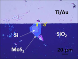
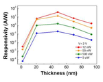
도 2는 본 발명의 일 실시예에 따라 제조된 Si-MoS2 포토다이오드의 광학현미경 사진이고, 도 3은 MoS2 두께에 따른 광반응성을 측정한 결과이다.
도 4는 본 발명의 일 실시예에 따라 제조한 포토다이오드의 MoS2 두께에 따른 저주파 노이즈 특성 분석결과이다.
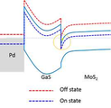
도 5는 본 발명의 2차원 반도체 기반의 MoS2-GaS 이종접합구조 기반 고속트랜지스터 소자의 에너지 밴드 다이어그램이다.
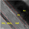
도 6은 MoS2-GaS 이종접합구조 고속트랜지스터 소자의 전자현미경 단면도이다.
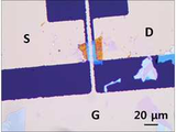
도 7은 MoS2-GaS 이종접합구조 고속트랜지스터 소자의 광학현미경 상면도이다.
도 8은 본 발명에 따른 MoS2-GaS 트랜지스터 I-V 특성 결과이다.
Claims (8)
- 이차원 반도체 소재; 및
상기 이차원 반도체 소재와 접하는 또 다른 이종 소재를 포함하며,
상기 이종 소재는 상기 이차원 반도체 소재와 상이한 타입의 불순물이 도핑되었거나, 상기 이차원 반도체 소재와 상이한 밴드 갭을 갖는 것을 특징으로 하는 전자소자. - 제 1항에 있어서,
상기 이차원 반도체 소재는 전이금속 칼코겐 화합물을 포함하는 것을 특징으로 하는 전자소자. - 제 2항에 있어서,
상기 또 다른 이종 소재는, 상기 이차원 반도체 소재와는 상이한 타입의 불순물이 도핑된 실리콘 기판이며, 상기 이차원 반도체 소재의 두께에 따라 상기 이차원 반도체 소재와 상기 실리콘 기판 간의 PN 접합에 따른 공핍층 두께가 제어되는 것을 특징으로 하는 전자소자. - 제 3항에 있어서,
상기 전자소자는 포토 다이오드인 것을 특징으로 하는 전자소자. - 제 1항에 있어서,
상기 이종소재는 상기 이차원 반도체 소재보다는 넓은 밴드갭을 갖는 반도체 소재인 것을 특징으로 하는 전자소자. - 제 5항에 있어서,
상기 전자소자는 트랜지스터이며, 상기 이차원 반도체 소재와 상기 이종소재 간의 상이한 밴드갭에 의하여 상기 트랜지스터에는 2차원 전자 가스(2DEG)가 형성된 것을 특징으로 하는 전자소자. - 제 6항에 있어서,
상기 이차원 반도체 소재는 MoS2, 상기 이종소재는 GaS이며, 상기 GaS는 상기 게이트 전극과 접하는 것을 특징으로 하는 전자소자. - 제 6항에 있어서,
상기 이종소재는 결정질이며, 상기 이종소재는 상기 게이트 전극으로 전기장 인가시 누설전류를 차단하는 절연성을 갖는 것을 특징으로 하는 전자소자.
Priority Applications (2)
| Application Number | Priority Date | Filing Date | Title |
|---|---|---|---|
| KR1020180162126A KR102153945B1 (ko) | 2018-12-14 | 2018-12-14 | 이차원 반도체 소재를 이용한 전자소자 |
| US16/226,950 US11024759B2 (en) | 2018-12-14 | 2018-12-20 | Electronic device using two dimensional semiconductor material |
Applications Claiming Priority (1)
| Application Number | Priority Date | Filing Date | Title |
|---|---|---|---|
| KR1020180162126A KR102153945B1 (ko) | 2018-12-14 | 2018-12-14 | 이차원 반도체 소재를 이용한 전자소자 |
Publications (2)
| Publication Number | Publication Date |
|---|---|
| KR20200073683A true KR20200073683A (ko) | 2020-06-24 |
| KR102153945B1 KR102153945B1 (ko) | 2020-09-09 |
Family
ID=71073739
Family Applications (1)
| Application Number | Title | Priority Date | Filing Date |
|---|---|---|---|
| KR1020180162126A Active KR102153945B1 (ko) | 2018-12-14 | 2018-12-14 | 이차원 반도체 소재를 이용한 전자소자 |
Country Status (2)
| Country | Link |
|---|---|
| US (1) | US11024759B2 (ko) |
| KR (1) | KR102153945B1 (ko) |
Cited By (1)
| Publication number | Priority date | Publication date | Assignee | Title |
|---|---|---|---|---|
| KR102678796B1 (ko) * | 2023-01-13 | 2024-06-26 | 주식회사 트루픽셀 | 단일 광자 검출기, 전자 장치, 및 라이다 장치 |
Families Citing this family (5)
| Publication number | Priority date | Publication date | Assignee | Title |
|---|---|---|---|---|
| CN109742178B (zh) * | 2019-01-29 | 2020-07-17 | 西安工业大学 | 一种透红外的高灵敏可见光探测器及其制备方法 |
| KR102542552B1 (ko) | 2021-08-02 | 2023-06-12 | 재단법인대구경북과학기술원 | 이종접합 광트랜지스터의 광전류 매핑 및 노이즈 전류 측정 장치 및 방법 |
| US20230110264A1 (en) * | 2021-09-09 | 2023-04-13 | The Regents Of The University Of California | Light-driven ultrafast electric gating |
| CN114464694B (zh) * | 2022-01-10 | 2024-05-28 | 华南师范大学 | 光电探测器及其制备方法 |
| KR102691495B1 (ko) * | 2022-08-24 | 2024-08-05 | 경상국립대학교산학협력단 | 다층 전이금속 디칼코게나이드 박막의 표면특성 및 두께 제어방법 |
Citations (1)
| Publication number | Priority date | Publication date | Assignee | Title |
|---|---|---|---|---|
| KR20170121961A (ko) * | 2016-04-26 | 2017-11-03 | 연세대학교 산학협력단 | 전이금속 디칼코게나이드와 금속 산화물 반도체를 이용한 pn 접합 다이오드 및 그 제조방법 |
Family Cites Families (6)
| Publication number | Priority date | Publication date | Assignee | Title |
|---|---|---|---|---|
| WO2013063399A1 (en) * | 2011-10-28 | 2013-05-02 | Georgetown University | Method and system for generating a photo-response from mos2 schottky junctions |
| JP2013110250A (ja) * | 2011-11-21 | 2013-06-06 | Toshiba Corp | 固体撮像装置及びその製造方法 |
| US20150108500A1 (en) * | 2013-10-18 | 2015-04-23 | Infineon Technologies Austria Ag | Semiconductor Device and Method of Manufacturing the Same |
| US9478419B2 (en) * | 2013-12-18 | 2016-10-25 | Asm Ip Holding B.V. | Sulfur-containing thin films |
| CN108461632A (zh) * | 2017-02-21 | 2018-08-28 | 华邦电子股份有限公司 | 钙钛矿复合结构 |
| US11133409B2 (en) * | 2018-10-17 | 2021-09-28 | The Research Foundation For The State University Of New York | Ballistic field-effect transistors based on Bloch resonance and methods of operating a transistor |
-
2018
- 2018-12-14 KR KR1020180162126A patent/KR102153945B1/ko active Active
- 2018-12-20 US US16/226,950 patent/US11024759B2/en active Active
Patent Citations (1)
| Publication number | Priority date | Publication date | Assignee | Title |
|---|---|---|---|---|
| KR20170121961A (ko) * | 2016-04-26 | 2017-11-03 | 연세대학교 산학협력단 | 전이금속 디칼코게나이드와 금속 산화물 반도체를 이용한 pn 접합 다이오드 및 그 제조방법 |
Cited By (3)
| Publication number | Priority date | Publication date | Assignee | Title |
|---|---|---|---|---|
| KR102678796B1 (ko) * | 2023-01-13 | 2024-06-26 | 주식회사 트루픽셀 | 단일 광자 검출기, 전자 장치, 및 라이다 장치 |
| US12099146B2 (en) | 2023-01-13 | 2024-09-24 | Trupixel Inc. | Single photon detector, electronic device, and LiDAR device |
| US12607723B2 (en) | 2023-01-13 | 2026-04-21 | Trupixel Inc. | Single photon detector, electronic device, and LiDAR device |
Also Published As
| Publication number | Publication date |
|---|---|
| KR102153945B1 (ko) | 2020-09-09 |
| US11024759B2 (en) | 2021-06-01 |
| US20200194602A1 (en) | 2020-06-18 |
Similar Documents
| Publication | Publication Date | Title |
|---|---|---|
| KR102153945B1 (ko) | 이차원 반도체 소재를 이용한 전자소자 | |
| TWI732925B (zh) | 與工程基板整合之電力元件 | |
| CN102244002B (zh) | 金属/半导体纳米线交叉结构异质结的制备方法 | |
| US20060145190A1 (en) | Surface passivation for III-V compound semiconductors | |
| EP3428957B1 (en) | Method for producing semiconductor device | |
| CN110660882B (zh) | 一种栅控PIN结构GaN紫外探测器及其制备方法 | |
| KR20160057343A (ko) | 질화갈륨(GaN) 고 전자이동도 트랜지스터용 구조체 | |
| CN107248530B (zh) | 一种二维材料/半导体异质结垂直隧穿晶体管及制备方法 | |
| TW201929044A (zh) | 用於工程基板上的整合裝置之系統及方法 | |
| KR102210325B1 (ko) | Cmos 소자 및 그 제조 방법 | |
| CN106549038A (zh) | 一种垂直结构的氮化镓异质结hemt | |
| CN103594419A (zh) | 半导体器件制造方法 | |
| CN102810555A (zh) | 一种锗锡隧穿场效应晶体管及其制备方法 | |
| JP6525554B2 (ja) | 基板構造体を含むcmos素子 | |
| JP2024545586A (ja) | シリコンオンインシュレータ上のiii族窒化物半導体構造およびそれを成長させる方法 | |
| CN114496788A (zh) | 一种p型沟道氮化镓晶体管及其制备方法 | |
| CN113972263B (zh) | 一种增强型AlGaN/GaN HEMT器件及其制备方法 | |
| CN115732566B (zh) | Umosfet器件及提高umosfet器件性能的方法 | |
| JP6531243B2 (ja) | トンネル電界効果トランジスタおよび電界効果トランジスタの製造方法 | |
| CN115911094A (zh) | 一种基于外延技术的三端铁电存储器及其制备方法 | |
| KR102485133B1 (ko) | 고효율 질화물계 광 검출기 | |
| CN111341840B (zh) | 场效应晶体管器件 | |
| CN117438457B (zh) | 凹槽栅型GaN基HEMT器件及其制备方法 | |
| KR20200076901A (ko) | 상이한 밴드갭을 갖는 이종 이차원 박막을 이용한 반도체 소자 | |
| CN115332249A (zh) | 晶体管及其制作方法 |
Legal Events
| Date | Code | Title | Description |
|---|---|---|---|
| PA0109 | Patent application |
St.27 status event code: A-0-1-A10-A12-nap-PA0109 |
|
| PA0201 | Request for examination |
St.27 status event code: A-1-2-D10-D11-exm-PA0201 |
|
| R18-X000 | Changes to party contact information recorded |
St.27 status event code: A-3-3-R10-R18-oth-X000 |
|
| D13-X000 | Search requested |
St.27 status event code: A-1-2-D10-D13-srh-X000 |
|
| D14-X000 | Search report completed |
St.27 status event code: A-1-2-D10-D14-srh-X000 |
|
| PE0902 | Notice of grounds for rejection |
St.27 status event code: A-1-2-D10-D21-exm-PE0902 |
|
| E13-X000 | Pre-grant limitation requested |
St.27 status event code: A-2-3-E10-E13-lim-X000 |
|
| P11-X000 | Amendment of application requested |
St.27 status event code: A-2-2-P10-P11-nap-X000 |
|
| P13-X000 | Application amended |
St.27 status event code: A-2-2-P10-P13-nap-X000 |
|
| PN2301 | Change of applicant |
St.27 status event code: A-3-3-R10-R13-asn-PN2301 St.27 status event code: A-3-3-R10-R11-asn-PN2301 |
|
| E701 | Decision to grant or registration of patent right | ||
| PE0701 | Decision of registration |
St.27 status event code: A-1-2-D10-D22-exm-PE0701 |
|
| R18-X000 | Changes to party contact information recorded |
St.27 status event code: A-3-3-R10-R18-oth-X000 |
|
| PG1501 | Laying open of application |
St.27 status event code: A-1-1-Q10-Q12-nap-PG1501 |
|
| GRNT | Written decision to grant | ||
| PR0701 | Registration of establishment |
St.27 status event code: A-2-4-F10-F11-exm-PR0701 |
|
| PR1002 | Payment of registration fee |
St.27 status event code: A-2-2-U10-U11-oth-PR1002 Fee payment year number: 1 |
|
| PG1601 | Publication of registration |
St.27 status event code: A-4-4-Q10-Q13-nap-PG1601 |
|
| R18-X000 | Changes to party contact information recorded |
St.27 status event code: A-5-5-R10-R18-oth-X000 |
|
| R18-X000 | Changes to party contact information recorded |
St.27 status event code: A-5-5-R10-R18-oth-X000 |
|
| PR1001 | Payment of annual fee |
St.27 status event code: A-4-4-U10-U11-oth-PR1001 Fee payment year number: 4 |
|
| PR1001 | Payment of annual fee |
St.27 status event code: A-4-4-U10-U11-oth-PR1001 Fee payment year number: 5 |
|
| P22-X000 | Classification modified |
St.27 status event code: A-4-4-P10-P22-nap-X000 |
|
| P22-X000 | Classification modified |
St.27 status event code: A-4-4-P10-P22-nap-X000 |