KR20200076264A - n-형 박막 트랜지스터를 인쇄하기 위한 n-형 도핑 잉크, n-형 도핑 잉크를 이용하여 n-형 박막 트랜지스터를 인쇄하는 방법 - Google Patents
n-형 박막 트랜지스터를 인쇄하기 위한 n-형 도핑 잉크, n-형 도핑 잉크를 이용하여 n-형 박막 트랜지스터를 인쇄하는 방법 Download PDFInfo
- Publication number
- KR20200076264A KR20200076264A KR1020180165193A KR20180165193A KR20200076264A KR 20200076264 A KR20200076264 A KR 20200076264A KR 1020180165193 A KR1020180165193 A KR 1020180165193A KR 20180165193 A KR20180165193 A KR 20180165193A KR 20200076264 A KR20200076264 A KR 20200076264A
- Authority
- KR
- South Korea
- Prior art keywords
- printing
- ink
- type
- type doping
- thin film
- Prior art date
- Legal status (The legal status is an assumption and is not a legal conclusion. Google has not performed a legal analysis and makes no representation as to the accuracy of the status listed.)
- Granted
Links
Images


Classifications
-
- C—CHEMISTRY; METALLURGY
- C09—DYES; PAINTS; POLISHES; NATURAL RESINS; ADHESIVES; COMPOSITIONS NOT OTHERWISE PROVIDED FOR; APPLICATIONS OF MATERIALS NOT OTHERWISE PROVIDED FOR
- C09D—COATING COMPOSITIONS, e.g. PAINTS, VARNISHES OR LACQUERS; FILLING PASTES; CHEMICAL PAINT OR INK REMOVERS; INKS; CORRECTING FLUIDS; WOODSTAINS; PASTES OR SOLIDS FOR COLOURING OR PRINTING; USE OF MATERIALS THEREFOR
- C09D11/00—Inks
- C09D11/02—Printing inks
- C09D11/03—Printing inks characterised by features other than the chemical nature of the binder
- C09D11/037—Printing inks characterised by features other than the chemical nature of the binder characterised by the pigment
-
- B—PERFORMING OPERATIONS; TRANSPORTING
- B41—PRINTING; LINING MACHINES; TYPEWRITERS; STAMPS
- B41M—PRINTING, DUPLICATING, MARKING, OR COPYING PROCESSES; COLOUR PRINTING
- B41M1/00—Inking and printing with a printer's forme
- B41M1/10—Intaglio printing ; Gravure printing
-
- C—CHEMISTRY; METALLURGY
- C09—DYES; PAINTS; POLISHES; NATURAL RESINS; ADHESIVES; COMPOSITIONS NOT OTHERWISE PROVIDED FOR; APPLICATIONS OF MATERIALS NOT OTHERWISE PROVIDED FOR
- C09D—COATING COMPOSITIONS, e.g. PAINTS, VARNISHES OR LACQUERS; FILLING PASTES; CHEMICAL PAINT OR INK REMOVERS; INKS; CORRECTING FLUIDS; WOODSTAINS; PASTES OR SOLIDS FOR COLOURING OR PRINTING; USE OF MATERIALS THEREFOR
- C09D11/00—Inks
- C09D11/02—Printing inks
- C09D11/03—Printing inks characterised by features other than the chemical nature of the binder
- C09D11/033—Printing inks characterised by features other than the chemical nature of the binder characterised by the solvent
-
- C—CHEMISTRY; METALLURGY
- C09—DYES; PAINTS; POLISHES; NATURAL RESINS; ADHESIVES; COMPOSITIONS NOT OTHERWISE PROVIDED FOR; APPLICATIONS OF MATERIALS NOT OTHERWISE PROVIDED FOR
- C09D—COATING COMPOSITIONS, e.g. PAINTS, VARNISHES OR LACQUERS; FILLING PASTES; CHEMICAL PAINT OR INK REMOVERS; INKS; CORRECTING FLUIDS; WOODSTAINS; PASTES OR SOLIDS FOR COLOURING OR PRINTING; USE OF MATERIALS THEREFOR
- C09D11/00—Inks
- C09D11/02—Printing inks
- C09D11/10—Printing inks based on artificial resins
-
- H01L21/02288—
-
- H01L29/66742—
-
- H01L29/78606—
-
- H01L29/78618—
-
- H—ELECTRICITY
- H10—SEMICONDUCTOR DEVICES; ELECTRIC SOLID-STATE DEVICES NOT OTHERWISE PROVIDED FOR
- H10D—INORGANIC ELECTRIC SEMICONDUCTOR DEVICES
- H10D30/00—Field-effect transistors [FET]
- H10D30/01—Manufacture or treatment
- H10D30/021—Manufacture or treatment of FETs having insulated gates [IGFET]
- H10D30/031—Manufacture or treatment of FETs having insulated gates [IGFET] of thin-film transistors [TFT]
-
- H—ELECTRICITY
- H10—SEMICONDUCTOR DEVICES; ELECTRIC SOLID-STATE DEVICES NOT OTHERWISE PROVIDED FOR
- H10D—INORGANIC ELECTRIC SEMICONDUCTOR DEVICES
- H10D30/00—Field-effect transistors [FET]
- H10D30/60—Insulated-gate field-effect transistors [IGFET]
- H10D30/67—Thin-film transistors [TFT]
-
- H—ELECTRICITY
- H10—SEMICONDUCTOR DEVICES; ELECTRIC SOLID-STATE DEVICES NOT OTHERWISE PROVIDED FOR
- H10D—INORGANIC ELECTRIC SEMICONDUCTOR DEVICES
- H10D30/00—Field-effect transistors [FET]
- H10D30/60—Insulated-gate field-effect transistors [IGFET]
- H10D30/67—Thin-film transistors [TFT]
- H10D30/6704—Thin-film transistors [TFT] having supplementary regions or layers in the thin films or in the insulated bulk substrates for controlling properties of the device
-
- H—ELECTRICITY
- H10—SEMICONDUCTOR DEVICES; ELECTRIC SOLID-STATE DEVICES NOT OTHERWISE PROVIDED FOR
- H10D—INORGANIC ELECTRIC SEMICONDUCTOR DEVICES
- H10D30/00—Field-effect transistors [FET]
- H10D30/60—Insulated-gate field-effect transistors [IGFET]
- H10D30/67—Thin-film transistors [TFT]
- H10D30/6704—Thin-film transistors [TFT] having supplementary regions or layers in the thin films or in the insulated bulk substrates for controlling properties of the device
- H10D30/6713—Thin-film transistors [TFT] having supplementary regions or layers in the thin films or in the insulated bulk substrates for controlling properties of the device characterised by the properties of the source or drain regions, e.g. compositions or sectional shapes
-
- H—ELECTRICITY
- H10—SEMICONDUCTOR DEVICES; ELECTRIC SOLID-STATE DEVICES NOT OTHERWISE PROVIDED FOR
- H10D—INORGANIC ELECTRIC SEMICONDUCTOR DEVICES
- H10D48/00—Individual devices not covered by groups H10D1/00 - H10D44/00
- H10D48/30—Devices controlled by electric currents or voltages
-
- H—ELECTRICITY
- H10—SEMICONDUCTOR DEVICES; ELECTRIC SOLID-STATE DEVICES NOT OTHERWISE PROVIDED FOR
- H10P—GENERIC PROCESSES OR APPARATUS FOR THE MANUFACTURE OR TREATMENT OF DEVICES COVERED BY CLASS H10
- H10P14/00—Formation of materials, e.g. in the shape of layers or pillars
- H10P14/60—Formation of materials, e.g. in the shape of layers or pillars of insulating materials
- H10P14/63—Formation of materials, e.g. in the shape of layers or pillars of insulating materials characterised by the formation processes
- H10P14/6326—Deposition processes
- H10P14/6342—Liquid deposition, e.g. spin-coating, sol-gel techniques or spray coating
- H10P14/6346—Liquid deposition, e.g. spin-coating, sol-gel techniques or spray coating using printing, e.g. ink-jet printing
-
- H—ELECTRICITY
- H10—SEMICONDUCTOR DEVICES; ELECTRIC SOLID-STATE DEVICES NOT OTHERWISE PROVIDED FOR
- H10P—GENERIC PROCESSES OR APPARATUS FOR THE MANUFACTURE OR TREATMENT OF DEVICES COVERED BY CLASS H10
- H10P95/00—Generic processes or apparatus for manufacture or treatments not covered by the other groups of this subclass
-
- H—ELECTRICITY
- H10—SEMICONDUCTOR DEVICES; ELECTRIC SOLID-STATE DEVICES NOT OTHERWISE PROVIDED FOR
- H10W—GENERIC PACKAGES, INTERCONNECTIONS, CONNECTORS OR OTHER CONSTRUCTIONAL DETAILS OF DEVICES COVERED BY CLASS H10
- H10W72/00—Interconnections or connectors in packages
- H10W72/01—Manufacture or treatment
- H10W72/0198—Manufacture or treatment batch processes
-
- H01L2224/95115—
Landscapes
- Chemical & Material Sciences (AREA)
- Life Sciences & Earth Sciences (AREA)
- Engineering & Computer Science (AREA)
- Materials Engineering (AREA)
- Wood Science & Technology (AREA)
- Organic Chemistry (AREA)
- Chemical Kinetics & Catalysis (AREA)
- General Chemical & Material Sciences (AREA)
- Thin Film Transistor (AREA)
- Electrodes Of Semiconductors (AREA)
- Inks, Pencil-Leads, Or Crayons (AREA)
Abstract
Description
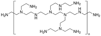
도 3은 본 발명에 따른 본 발명에 따른 n-형 도핑 잉크의 재료가 되는 고분자 에틸렌이민의 화학구조도이다.
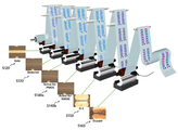
도 4는 본 발명의 일 실시예에 따른 n-형 도핑 잉크의 인쇄 특성을 설명하기 위한 도면이다.
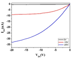
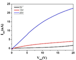
도 5 및 도 6은 본 발명에 따라 인쇄된 p-형 박막 트랜지스터의 n-형 박막 트랜지스터의 전압-전류 특성 그래프들이다.
Claims (8)
- 용매 부틸캐비톨(Diethylene glycol monobutyl ether)에 곁가지가 붙은 고분자 에틸렌이민과, TiO2, ZnO, 및 IGZO 나노 입자 중 적어도 하나를 혼합하여 제조되는 것을 특징으로 하는 n-형 도핑 잉크.
- 제1항에 있어서,
상기 곁가지가 붙은 고분자 에틸렌이민을 2.5 내지 10 wt% 혼합하고, 상기 TiO2 나노 입자를 1 wt% 혼합하여 제조되는 것을 특징으로 하는 n-형 도핑 잉크. - 아이소프로필 알코올(Isopropyl alcohol) 및 DMSO(Dimethyl sulfoxide)를 1:1의 부피비로 하여 용매를 제조하고, 상기 용매에 곁가지가 붙은 고분자 에틸렌이민과, TiO2, ZnO, 및 IGZO 나노 입자 중 적어도 하나를 혼합하여 제조되는 것을 특징으로 하는 n-형 도핑 잉크.
- 제3항에 있어서,
상기 곁가지가 붙은 고분자 에틸렌이민을 2.5 내지 10 wt% 혼합하고, 상기 TiO2 나노 입자를 1 wt% 혼합하여 제조되는 것을 특징으로 하는 n-형 도핑 잉크. - 제1항 내지 제4항 중 어느 한 항에 있어서,
상기 곁가지가 붙은 고분자 에틸렌이민과 선형 고분자 에틸렌이민을 함께 사용하여 제조되는 것을 특징으로 하는 n-형 도핑 잉크. - R2R(Roll-to-Roll) 또는 S2S(Sheet-to-Sheet) 그라비아 인쇄 방식으로 n-형 박막 트랜지스터를 인쇄하는 방법에 있어서,
게이트 전극을 포함한 제1 전도성 배선을, 실버 잉크를 사용하여 인쇄하는 단계;
상기 전도성 배선 상에 절연층을 인쇄하는 단계;
상기 절연층 상에 활성층을 인쇄하는 단계;
상기 활성층 상에 소스 및 드레인 전극들을 포함한 제2 전도성 배선을, 실버 잉크를 사용하여 인쇄하는 단계; 및
곁가지가 붙은 고분자 에틸렌이민과, TiO2, ZnO, 및 IGZO 나노 입자 중 적어도 하나를 용매 부틸캐비톨에 혼합하여 제조된 n-형 도핑 잉크를, 점도 5 내지 200 센티포이즈(cP)를 가지도록 하면서 표면장력을 30mN/m 이하로 제어하여 그라비아 인쇄를 수행하는 단계를 포함하는 것을 특징으로 하는, n-형 박막 트랜지스터 인쇄 방법. - 제6항에 있어서,
상기 n-형 도핑 잉크는 곁가지가 붙은 고분자 에틸렌이민을 2.5 내지 10 wt%로, 상기 TiO2 나노 입자를 1 wt%로, 상기 용매에 혼합하여 제조되는 것을 특징으로 하는, n-형 박막 트랜지스터 인쇄 방법. - 제7항에 있어서,
상기 n-형 도핑 잉크를 인쇄하는 단계는,
상기 소스 및 드레인 전극 사이에 노출된 상기 활성층 상에 상기 n-형 도핑 잉크를 인쇄하는 단계를 포함하는 것을 특징으로 하는, n-형 박막 트랜지스터 인쇄 방법.
Priority Applications (2)
| Application Number | Priority Date | Filing Date | Title |
|---|---|---|---|
| PCT/KR2018/016272 WO2020130187A1 (ko) | 2018-12-19 | 2018-12-19 | N-형 박막 트랜지스터를 인쇄하기 위한 n-형 도핑 잉크, n-형 도핑 잉크를 이용하여 n-형 박막 트랜지스터를 인쇄하는 방법 |
| KR1020180165193A KR102242468B1 (ko) | 2018-12-19 | 2018-12-19 | n-형 박막 트랜지스터를 인쇄하기 위한 n-형 도핑 잉크, n-형 도핑 잉크를 이용하여 n-형 박막 트랜지스터를 인쇄하는 방법 |
Applications Claiming Priority (1)
| Application Number | Priority Date | Filing Date | Title |
|---|---|---|---|
| KR1020180165193A KR102242468B1 (ko) | 2018-12-19 | 2018-12-19 | n-형 박막 트랜지스터를 인쇄하기 위한 n-형 도핑 잉크, n-형 도핑 잉크를 이용하여 n-형 박막 트랜지스터를 인쇄하는 방법 |
Publications (2)
| Publication Number | Publication Date |
|---|---|
| KR20200076264A true KR20200076264A (ko) | 2020-06-29 |
| KR102242468B1 KR102242468B1 (ko) | 2021-04-20 |
Family
ID=71102225
Family Applications (1)
| Application Number | Title | Priority Date | Filing Date |
|---|---|---|---|
| KR1020180165193A Active KR102242468B1 (ko) | 2018-12-19 | 2018-12-19 | n-형 박막 트랜지스터를 인쇄하기 위한 n-형 도핑 잉크, n-형 도핑 잉크를 이용하여 n-형 박막 트랜지스터를 인쇄하는 방법 |
Country Status (2)
| Country | Link |
|---|---|
| KR (1) | KR102242468B1 (ko) |
| WO (1) | WO2020130187A1 (ko) |
Citations (5)
| Publication number | Priority date | Publication date | Assignee | Title |
|---|---|---|---|---|
| US6231655B1 (en) * | 1999-03-19 | 2001-05-15 | Seiko Epson Corporation | Aqueous ink composition for use in an ink jet printer |
| KR20080001654A (ko) * | 2006-06-29 | 2008-01-03 | 주식회사 엘지화학 | 폴리에틸렌이민 화합물을 포함하는 회로 배선용 금속 나노잉크 |
| KR20080016170A (ko) * | 2006-08-18 | 2008-02-21 | 제이에스알 가부시끼가이샤 | 안료 수지 조성물, 잉크 제트 방식의 칼라 필터용 수지조성물, 칼라 필터, 및 액정 표시 장치 |
| KR20160062773A (ko) * | 2014-11-25 | 2016-06-03 | 순천대학교 산학협력단 | 롤대롤 그라비아 인쇄기반 박막트랜지스터 제조방법, 박막트랜지스터 백플랜 제조방법, 백플랜 압력센서 및 스마트 장판의 제조방법 |
| US20170092865A1 (en) * | 2015-09-30 | 2017-03-30 | LI Yuning | N-type organic semiconductor formulations and devices |
-
2018
- 2018-12-19 KR KR1020180165193A patent/KR102242468B1/ko active Active
- 2018-12-19 WO PCT/KR2018/016272 patent/WO2020130187A1/ko not_active Ceased
Patent Citations (5)
| Publication number | Priority date | Publication date | Assignee | Title |
|---|---|---|---|---|
| US6231655B1 (en) * | 1999-03-19 | 2001-05-15 | Seiko Epson Corporation | Aqueous ink composition for use in an ink jet printer |
| KR20080001654A (ko) * | 2006-06-29 | 2008-01-03 | 주식회사 엘지화학 | 폴리에틸렌이민 화합물을 포함하는 회로 배선용 금속 나노잉크 |
| KR20080016170A (ko) * | 2006-08-18 | 2008-02-21 | 제이에스알 가부시끼가이샤 | 안료 수지 조성물, 잉크 제트 방식의 칼라 필터용 수지조성물, 칼라 필터, 및 액정 표시 장치 |
| KR20160062773A (ko) * | 2014-11-25 | 2016-06-03 | 순천대학교 산학협력단 | 롤대롤 그라비아 인쇄기반 박막트랜지스터 제조방법, 박막트랜지스터 백플랜 제조방법, 백플랜 압력센서 및 스마트 장판의 제조방법 |
| US20170092865A1 (en) * | 2015-09-30 | 2017-03-30 | LI Yuning | N-type organic semiconductor formulations and devices |
Also Published As
| Publication number | Publication date |
|---|---|
| KR102242468B1 (ko) | 2021-04-20 |
| WO2020130187A1 (ko) | 2020-06-25 |
Similar Documents
| Publication | Publication Date | Title |
|---|---|---|
| Chen et al. | Large-scale complementary macroelectronics using hybrid integration of carbon nanotubes and IGZO thin-film transistors | |
| Yu et al. | Fully printed flexible dual-gate carbon nanotube thin-film transistors with tunable ambipolar characteristics for complementary logic circuits | |
| Chang et al. | Solution-processed transparent blue organic light-emitting diodes with graphene as the top cathode | |
| JP4572543B2 (ja) | 電界効果型トランジスタ並びにそれを用いた液晶表示装置 | |
| Kim et al. | Inkjet printed circuits on flexible and rigid substrates based on ambipolar carbon nanotubes with high operational stability | |
| Shiwaku et al. | Printed 2 V-operating organic inverter arrays employing a small-molecule/polymer blend | |
| JP4730623B2 (ja) | 薄膜トランジスタ、薄膜トランジスタの製造方法、および電子機器 | |
| Kang et al. | Megahertz-class printed high mobility organic thin-film transistors and inverters on plastic using attoliter-scale high-speed gravure-printed sub-5 μm gate electrodes | |
| CN105393312B (zh) | 铜和/或铜氧化物分散体、以及使用该分散体形成的导电膜 | |
| Pei et al. | Understanding molecular surface doping of large bandgap organic semiconductors and overcoming the contact/access resistance in organic field-effect transistors | |
| US9564481B2 (en) | Fully-printed carbon nanotube thin film transistor circuits for organic light emitting diode | |
| JP2006186294A (ja) | 薄膜トランジスタ及びその製造方法 | |
| Chen et al. | Thin dielectric-layer-enabled low-voltage operation of fully printed flexible carbon nanotube thin-film transistors | |
| Guo et al. | Insights into the device structure, processing and material design for an organic thin-film transistor towards functional circuit integration | |
| US11195886B2 (en) | Organic light emitting diode and three-dimensional tactile display apparatus using stretchable light-emitting material and manufacturing method thereof | |
| CN104362176A (zh) | 高开关比的自对准双栅小带隙半导体晶体管及制备方法 | |
| JP5382763B2 (ja) | 半導体素子及びその製造方法と、該半導体素子を備えた電子デバイス | |
| Li et al. | Printed flexible thin-film transistors based on different types of modified liquid metal with good mobility | |
| Kim et al. | Enhanced performance and reliability of organic thin film transistors through structural scaling in gravure printing process | |
| KR101487443B1 (ko) | 유전막 표면 개질용 트랜지스터 및 이의 제조 방법 | |
| JP2009065057A (ja) | 半導体装置 | |
| KR102242468B1 (ko) | n-형 박막 트랜지스터를 인쇄하기 위한 n-형 도핑 잉크, n-형 도핑 잉크를 이용하여 n-형 박막 트랜지스터를 인쇄하는 방법 | |
| Jiang et al. | All-inkjet-printed high-performance flexible MoS2 and MoS2-reduced graphene oxide field-effect transistors | |
| Chen et al. | Locally Doped Transferred Contacts for WSe2 Transistors | |
| US20060081816A1 (en) | Material for the production of a conductive organic funtional layer and use thereof |
Legal Events
| Date | Code | Title | Description |
|---|---|---|---|
| PA0109 | Patent application |
St.27 status event code: A-0-1-A10-A12-nap-PA0109 |
|
| PA0201 | Request for examination |
St.27 status event code: A-1-2-D10-D11-exm-PA0201 |
|
| D13-X000 | Search requested |
St.27 status event code: A-1-2-D10-D13-srh-X000 |
|
| D14-X000 | Search report completed |
St.27 status event code: A-1-2-D10-D14-srh-X000 |
|
| N231 | Notification of change of applicant | ||
| PN2301 | Change of applicant |
St.27 status event code: A-3-3-R10-R13-asn-PN2301 St.27 status event code: A-3-3-R10-R11-asn-PN2301 |
|
| R17-X000 | Change to representative recorded |
St.27 status event code: A-3-3-R10-R17-oth-X000 |
|
| PG1501 | Laying open of application |
St.27 status event code: A-1-1-Q10-Q12-nap-PG1501 |
|
| E902 | Notification of reason for refusal | ||
| PE0902 | Notice of grounds for rejection |
St.27 status event code: A-1-2-D10-D21-exm-PE0902 |
|
| T11-X000 | Administrative time limit extension requested |
St.27 status event code: U-3-3-T10-T11-oth-X000 |
|
| T11-X000 | Administrative time limit extension requested |
St.27 status event code: U-3-3-T10-T11-oth-X000 |
|
| E13-X000 | Pre-grant limitation requested |
St.27 status event code: A-2-3-E10-E13-lim-X000 |
|
| P11-X000 | Amendment of application requested |
St.27 status event code: A-2-2-P10-P11-nap-X000 |
|
| P13-X000 | Application amended |
St.27 status event code: A-2-2-P10-P13-nap-X000 |
|
| E902 | Notification of reason for refusal | ||
| PE0902 | Notice of grounds for rejection |
St.27 status event code: A-1-2-D10-D21-exm-PE0902 |
|
| P11-X000 | Amendment of application requested |
St.27 status event code: A-2-2-P10-P11-nap-X000 |
|
| P13-X000 | Application amended |
St.27 status event code: A-2-2-P10-P13-nap-X000 |
|
| E701 | Decision to grant or registration of patent right | ||
| PE0701 | Decision of registration |
St.27 status event code: A-1-2-D10-D22-exm-PE0701 |
|
| GRNT | Written decision to grant | ||
| PR0701 | Registration of establishment |
St.27 status event code: A-2-4-F10-F11-exm-PR0701 |
|
| PR1002 | Payment of registration fee |
St.27 status event code: A-2-2-U10-U11-oth-PR1002 Fee payment year number: 1 |
|
| PG1601 | Publication of registration |
St.27 status event code: A-4-4-Q10-Q13-nap-PG1601 |
|
| R18-X000 | Changes to party contact information recorded |
St.27 status event code: A-5-5-R10-R18-oth-X000 |
|
| PR1001 | Payment of annual fee |
St.27 status event code: A-4-4-U10-U11-oth-PR1001 Fee payment year number: 4 |
|
| PN2301 | Change of applicant |
St.27 status event code: A-5-5-R10-R13-asn-PN2301 St.27 status event code: A-5-5-R10-R11-asn-PN2301 |
|
| PR1001 | Payment of annual fee |
St.27 status event code: A-4-4-U10-U11-oth-PR1001 Fee payment year number: 5 |
|
| P22-X000 | Classification modified |
St.27 status event code: A-4-4-P10-P22-nap-X000 |
|
| R18-X000 | Changes to party contact information recorded |
St.27 status event code: A-5-5-R10-R18-oth-X000 |
|
| PR1001 | Payment of annual fee |
St.27 status event code: A-4-4-U10-U11-oth-PR1001 Fee payment year number: 6 |
|
| U11 | Full renewal or maintenance fee paid |
Free format text: ST27 STATUS EVENT CODE: A-4-4-U10-U11-OTH-PR1001 (AS PROVIDED BY THE NATIONAL OFFICE) Year of fee payment: 6 |
|
| P22-X000 | Classification modified |
St.27 status event code: A-4-4-P10-P22-nap-X000 |
|
| P22-X000 | Classification modified |
St.27 status event code: A-4-4-P10-P22-nap-X000 |