KR20200076684A - 막형성 기재의 제조 방법, 막형성 기재 및 표면 처리제 - Google Patents
막형성 기재의 제조 방법, 막형성 기재 및 표면 처리제 Download PDFInfo
- Publication number
- KR20200076684A KR20200076684A KR1020207010911A KR20207010911A KR20200076684A KR 20200076684 A KR20200076684 A KR 20200076684A KR 1020207010911 A KR1020207010911 A KR 1020207010911A KR 20207010911 A KR20207010911 A KR 20207010911A KR 20200076684 A KR20200076684 A KR 20200076684A
- Authority
- KR
- South Korea
- Prior art keywords
- film
- metal substrate
- forming
- substrate
- surface treatment
- Prior art date
- Legal status (The legal status is an assumption and is not a legal conclusion. Google has not performed a legal analysis and makes no representation as to the accuracy of the status listed.)
- Granted
Links
Images


Classifications
-
- B—PERFORMING OPERATIONS; TRANSPORTING
- B05—SPRAYING OR ATOMISING IN GENERAL; APPLYING FLUENT MATERIALS TO SURFACES, IN GENERAL
- B05D—PROCESSES FOR APPLYING FLUENT MATERIALS TO SURFACES, IN GENERAL
- B05D7/00—Processes, other than flocking, specially adapted for applying liquids or other fluent materials to particular surfaces or for applying particular liquids or other fluent materials
- B05D7/14—Processes, other than flocking, specially adapted for applying liquids or other fluent materials to particular surfaces or for applying particular liquids or other fluent materials to metal, e.g. car bodies
-
- B—PERFORMING OPERATIONS; TRANSPORTING
- B05—SPRAYING OR ATOMISING IN GENERAL; APPLYING FLUENT MATERIALS TO SURFACES, IN GENERAL
- B05D—PROCESSES FOR APPLYING FLUENT MATERIALS TO SURFACES, IN GENERAL
- B05D1/00—Processes for applying liquids or other fluent materials
- B05D1/02—Processes for applying liquids or other fluent materials performed by spraying
-
- B—PERFORMING OPERATIONS; TRANSPORTING
- B05—SPRAYING OR ATOMISING IN GENERAL; APPLYING FLUENT MATERIALS TO SURFACES, IN GENERAL
- B05D—PROCESSES FOR APPLYING FLUENT MATERIALS TO SURFACES, IN GENERAL
- B05D3/00—Pretreatment of surfaces to which liquids or other fluent materials are to be applied; After-treatment of applied coatings, e.g. intermediate treating of an applied coating preparatory to subsequent applications of liquids or other fluent materials
- B05D3/10—Pretreatment of surfaces to which liquids or other fluent materials are to be applied; After-treatment of applied coatings, e.g. intermediate treating of an applied coating preparatory to subsequent applications of liquids or other fluent materials by other chemical means
- B05D3/102—Pretreatment of metallic substrates
-
- B—PERFORMING OPERATIONS; TRANSPORTING
- B05—SPRAYING OR ATOMISING IN GENERAL; APPLYING FLUENT MATERIALS TO SURFACES, IN GENERAL
- B05D—PROCESSES FOR APPLYING FLUENT MATERIALS TO SURFACES, IN GENERAL
- B05D3/00—Pretreatment of surfaces to which liquids or other fluent materials are to be applied; After-treatment of applied coatings, e.g. intermediate treating of an applied coating preparatory to subsequent applications of liquids or other fluent materials
- B05D3/12—Pretreatment of surfaces to which liquids or other fluent materials are to be applied; After-treatment of applied coatings, e.g. intermediate treating of an applied coating preparatory to subsequent applications of liquids or other fluent materials by mechanical means
-
- C—CHEMISTRY; METALLURGY
- C09—DYES; PAINTS; POLISHES; NATURAL RESINS; ADHESIVES; COMPOSITIONS NOT OTHERWISE PROVIDED FOR; APPLICATIONS OF MATERIALS NOT OTHERWISE PROVIDED FOR
- C09D—COATING COMPOSITIONS, e.g. PAINTS, VARNISHES OR LACQUERS; FILLING PASTES; CHEMICAL PAINT OR INK REMOVERS; INKS; CORRECTING FLUIDS; WOODSTAINS; PASTES OR SOLIDS FOR COLOURING OR PRINTING; USE OF MATERIALS THEREFOR
- C09D11/00—Inks
- C09D11/30—Inkjet printing inks
-
- C—CHEMISTRY; METALLURGY
- C23—COATING METALLIC MATERIAL; COATING MATERIAL WITH METALLIC MATERIAL; CHEMICAL SURFACE TREATMENT; DIFFUSION TREATMENT OF METALLIC MATERIAL; COATING BY VACUUM EVAPORATION, BY SPUTTERING, BY ION IMPLANTATION OR BY CHEMICAL VAPOUR DEPOSITION, IN GENERAL; INHIBITING CORROSION OF METALLIC MATERIAL OR INCRUSTATION IN GENERAL
- C23C—COATING METALLIC MATERIAL; COATING MATERIAL WITH METALLIC MATERIAL; SURFACE TREATMENT OF METALLIC MATERIAL BY DIFFUSION INTO THE SURFACE, BY CHEMICAL CONVERSION OR SUBSTITUTION; COATING BY VACUUM EVAPORATION, BY SPUTTERING, BY ION IMPLANTATION OR BY CHEMICAL VAPOUR DEPOSITION, IN GENERAL
- C23C22/00—Chemical surface treatment of metallic material by reaction of the surface with a reactive liquid, leaving reaction products of surface material in the coating, e.g. conversion coatings, passivation of metals
- C23C22/05—Chemical surface treatment of metallic material by reaction of the surface with a reactive liquid, leaving reaction products of surface material in the coating, e.g. conversion coatings, passivation of metals using aqueous solutions
- C23C22/06—Chemical surface treatment of metallic material by reaction of the surface with a reactive liquid, leaving reaction products of surface material in the coating, e.g. conversion coatings, passivation of metals using aqueous solutions using aqueous acidic solutions with pH less than 6
- C23C22/24—Chemical surface treatment of metallic material by reaction of the surface with a reactive liquid, leaving reaction products of surface material in the coating, e.g. conversion coatings, passivation of metals using aqueous solutions using aqueous acidic solutions with pH less than 6 containing hexavalent chromium compounds
- C23C22/26—Chemical surface treatment of metallic material by reaction of the surface with a reactive liquid, leaving reaction products of surface material in the coating, e.g. conversion coatings, passivation of metals using aqueous solutions using aqueous acidic solutions with pH less than 6 containing hexavalent chromium compounds containing also organic compounds
-
- C—CHEMISTRY; METALLURGY
- C23—COATING METALLIC MATERIAL; COATING MATERIAL WITH METALLIC MATERIAL; CHEMICAL SURFACE TREATMENT; DIFFUSION TREATMENT OF METALLIC MATERIAL; COATING BY VACUUM EVAPORATION, BY SPUTTERING, BY ION IMPLANTATION OR BY CHEMICAL VAPOUR DEPOSITION, IN GENERAL; INHIBITING CORROSION OF METALLIC MATERIAL OR INCRUSTATION IN GENERAL
- C23C—COATING METALLIC MATERIAL; COATING MATERIAL WITH METALLIC MATERIAL; SURFACE TREATMENT OF METALLIC MATERIAL BY DIFFUSION INTO THE SURFACE, BY CHEMICAL CONVERSION OR SUBSTITUTION; COATING BY VACUUM EVAPORATION, BY SPUTTERING, BY ION IMPLANTATION OR BY CHEMICAL VAPOUR DEPOSITION, IN GENERAL
- C23C22/00—Chemical surface treatment of metallic material by reaction of the surface with a reactive liquid, leaving reaction products of surface material in the coating, e.g. conversion coatings, passivation of metals
- C23C22/05—Chemical surface treatment of metallic material by reaction of the surface with a reactive liquid, leaving reaction products of surface material in the coating, e.g. conversion coatings, passivation of metals using aqueous solutions
- C23C22/06—Chemical surface treatment of metallic material by reaction of the surface with a reactive liquid, leaving reaction products of surface material in the coating, e.g. conversion coatings, passivation of metals using aqueous solutions using aqueous acidic solutions with pH less than 6
- C23C22/48—Chemical surface treatment of metallic material by reaction of the surface with a reactive liquid, leaving reaction products of surface material in the coating, e.g. conversion coatings, passivation of metals using aqueous solutions using aqueous acidic solutions with pH less than 6 not containing phosphates, hexavalent chromium compounds, fluorides or complex fluorides, molybdates, tungstates, vanadates or oxalates
- C23C22/52—Treatment of copper or alloys based thereon
-
- C—CHEMISTRY; METALLURGY
- C23—COATING METALLIC MATERIAL; COATING MATERIAL WITH METALLIC MATERIAL; CHEMICAL SURFACE TREATMENT; DIFFUSION TREATMENT OF METALLIC MATERIAL; COATING BY VACUUM EVAPORATION, BY SPUTTERING, BY ION IMPLANTATION OR BY CHEMICAL VAPOUR DEPOSITION, IN GENERAL; INHIBITING CORROSION OF METALLIC MATERIAL OR INCRUSTATION IN GENERAL
- C23C—COATING METALLIC MATERIAL; COATING MATERIAL WITH METALLIC MATERIAL; SURFACE TREATMENT OF METALLIC MATERIAL BY DIFFUSION INTO THE SURFACE, BY CHEMICAL CONVERSION OR SUBSTITUTION; COATING BY VACUUM EVAPORATION, BY SPUTTERING, BY ION IMPLANTATION OR BY CHEMICAL VAPOUR DEPOSITION, IN GENERAL
- C23C22/00—Chemical surface treatment of metallic material by reaction of the surface with a reactive liquid, leaving reaction products of surface material in the coating, e.g. conversion coatings, passivation of metals
- C23C22/05—Chemical surface treatment of metallic material by reaction of the surface with a reactive liquid, leaving reaction products of surface material in the coating, e.g. conversion coatings, passivation of metals using aqueous solutions
- C23C22/60—Chemical surface treatment of metallic material by reaction of the surface with a reactive liquid, leaving reaction products of surface material in the coating, e.g. conversion coatings, passivation of metals using aqueous solutions using alkaline aqueous solutions with pH greater than 8
- C23C22/63—Treatment of copper or alloys based thereon
-
- C—CHEMISTRY; METALLURGY
- C23—COATING METALLIC MATERIAL; COATING MATERIAL WITH METALLIC MATERIAL; CHEMICAL SURFACE TREATMENT; DIFFUSION TREATMENT OF METALLIC MATERIAL; COATING BY VACUUM EVAPORATION, BY SPUTTERING, BY ION IMPLANTATION OR BY CHEMICAL VAPOUR DEPOSITION, IN GENERAL; INHIBITING CORROSION OF METALLIC MATERIAL OR INCRUSTATION IN GENERAL
- C23C—COATING METALLIC MATERIAL; COATING MATERIAL WITH METALLIC MATERIAL; SURFACE TREATMENT OF METALLIC MATERIAL BY DIFFUSION INTO THE SURFACE, BY CHEMICAL CONVERSION OR SUBSTITUTION; COATING BY VACUUM EVAPORATION, BY SPUTTERING, BY ION IMPLANTATION OR BY CHEMICAL VAPOUR DEPOSITION, IN GENERAL
- C23C22/00—Chemical surface treatment of metallic material by reaction of the surface with a reactive liquid, leaving reaction products of surface material in the coating, e.g. conversion coatings, passivation of metals
- C23C22/05—Chemical surface treatment of metallic material by reaction of the surface with a reactive liquid, leaving reaction products of surface material in the coating, e.g. conversion coatings, passivation of metals using aqueous solutions
- C23C22/68—Chemical surface treatment of metallic material by reaction of the surface with a reactive liquid, leaving reaction products of surface material in the coating, e.g. conversion coatings, passivation of metals using aqueous solutions using aqueous solutions with pH between 6 and 8
-
- H—ELECTRICITY
- H05—ELECTRIC TECHNIQUES NOT OTHERWISE PROVIDED FOR
- H05K—PRINTED CIRCUITS; CASINGS OR CONSTRUCTIONAL DETAILS OF ELECTRIC APPARATUS; MANUFACTURE OF ASSEMBLAGES OF ELECTRICAL COMPONENTS
- H05K3/00—Apparatus or processes for manufacturing printed circuits
- H05K3/02—Apparatus or processes for manufacturing printed circuits in which the conductive material is applied to the surface of the insulating support and is thereafter removed from such areas of the surface which are not intended for current conducting or shielding
- H05K3/06—Apparatus or processes for manufacturing printed circuits in which the conductive material is applied to the surface of the insulating support and is thereafter removed from such areas of the surface which are not intended for current conducting or shielding the conductive material being removed chemically or electrolytically, e.g. by photo-etch process
-
- H—ELECTRICITY
- H05—ELECTRIC TECHNIQUES NOT OTHERWISE PROVIDED FOR
- H05K—PRINTED CIRCUITS; CASINGS OR CONSTRUCTIONAL DETAILS OF ELECTRIC APPARATUS; MANUFACTURE OF ASSEMBLAGES OF ELECTRICAL COMPONENTS
- H05K3/00—Apparatus or processes for manufacturing printed circuits
- H05K3/38—Improvement of the adhesion between the insulating substrate and the metal
- H05K3/381—Improvement of the adhesion between the insulating substrate and the metal by special treatment of the substrate
-
- H—ELECTRICITY
- H05—ELECTRIC TECHNIQUES NOT OTHERWISE PROVIDED FOR
- H05K—PRINTED CIRCUITS; CASINGS OR CONSTRUCTIONAL DETAILS OF ELECTRIC APPARATUS; MANUFACTURE OF ASSEMBLAGES OF ELECTRICAL COMPONENTS
- H05K3/00—Apparatus or processes for manufacturing printed circuits
- H05K3/38—Improvement of the adhesion between the insulating substrate and the metal
- H05K3/382—Improvement of the adhesion between the insulating substrate and the metal by special treatment of the metal
- H05K3/383—Improvement of the adhesion between the insulating substrate and the metal by special treatment of the metal by microetching
-
- B—PERFORMING OPERATIONS; TRANSPORTING
- B05—SPRAYING OR ATOMISING IN GENERAL; APPLYING FLUENT MATERIALS TO SURFACES, IN GENERAL
- B05D—PROCESSES FOR APPLYING FLUENT MATERIALS TO SURFACES, IN GENERAL
- B05D1/00—Processes for applying liquids or other fluent materials
- B05D1/26—Processes for applying liquids or other fluent materials performed by applying the liquid or other fluent material from an outlet device in contact with, or almost in contact with, the surface
-
- B—PERFORMING OPERATIONS; TRANSPORTING
- B05—SPRAYING OR ATOMISING IN GENERAL; APPLYING FLUENT MATERIALS TO SURFACES, IN GENERAL
- B05D—PROCESSES FOR APPLYING FLUENT MATERIALS TO SURFACES, IN GENERAL
- B05D2202/00—Metallic substrate
- B05D2202/40—Metallic substrate based on other transition elements
- B05D2202/45—Metallic substrate based on other transition elements based on Cu
-
- H—ELECTRICITY
- H05—ELECTRIC TECHNIQUES NOT OTHERWISE PROVIDED FOR
- H05K—PRINTED CIRCUITS; CASINGS OR CONSTRUCTIONAL DETAILS OF ELECTRIC APPARATUS; MANUFACTURE OF ASSEMBLAGES OF ELECTRICAL COMPONENTS
- H05K2201/00—Indexing scheme relating to printed circuits covered by H05K1/00
- H05K2201/01—Dielectrics
- H05K2201/0137—Materials
- H05K2201/0179—Thin film deposited insulating layer, e.g. inorganic layer for printed capacitor
-
- H—ELECTRICITY
- H05—ELECTRIC TECHNIQUES NOT OTHERWISE PROVIDED FOR
- H05K—PRINTED CIRCUITS; CASINGS OR CONSTRUCTIONAL DETAILS OF ELECTRIC APPARATUS; MANUFACTURE OF ASSEMBLAGES OF ELECTRICAL COMPONENTS
- H05K2203/00—Indexing scheme relating to apparatus or processes for manufacturing printed circuits covered by H05K3/00
- H05K2203/01—Tools for processing; Objects used during processing
- H05K2203/0104—Tools for processing; Objects used during processing for patterning or coating
- H05K2203/013—Inkjet printing, e.g. for printing insulating material or resist
-
- H—ELECTRICITY
- H05—ELECTRIC TECHNIQUES NOT OTHERWISE PROVIDED FOR
- H05K—PRINTED CIRCUITS; CASINGS OR CONSTRUCTIONAL DETAILS OF ELECTRIC APPARATUS; MANUFACTURE OF ASSEMBLAGES OF ELECTRICAL COMPONENTS
- H05K2203/00—Indexing scheme relating to apparatus or processes for manufacturing printed circuits covered by H05K3/00
- H05K2203/03—Metal processing
- H05K2203/0307—Providing micro- or nanometer scale roughness on a metal surface, e.g. by plating of nodules or dendrites
-
- H—ELECTRICITY
- H05—ELECTRIC TECHNIQUES NOT OTHERWISE PROVIDED FOR
- H05K—PRINTED CIRCUITS; CASINGS OR CONSTRUCTIONAL DETAILS OF ELECTRIC APPARATUS; MANUFACTURE OF ASSEMBLAGES OF ELECTRICAL COMPONENTS
- H05K2203/00—Indexing scheme relating to apparatus or processes for manufacturing printed circuits covered by H05K3/00
- H05K2203/03—Metal processing
- H05K2203/0369—Etching selective parts of a metal substrate through part of its thickness, e.g. using etch resist
-
- H—ELECTRICITY
- H05—ELECTRIC TECHNIQUES NOT OTHERWISE PROVIDED FOR
- H05K—PRINTED CIRCUITS; CASINGS OR CONSTRUCTIONAL DETAILS OF ELECTRIC APPARATUS; MANUFACTURE OF ASSEMBLAGES OF ELECTRICAL COMPONENTS
- H05K3/00—Apparatus or processes for manufacturing printed circuits
- H05K3/22—Secondary treatment of printed circuits
- H05K3/28—Applying non-metallic protective coatings
- H05K3/282—Applying non-metallic protective coatings for inhibiting the corrosion of the circuit, e.g. for preserving the solderability
Landscapes
- Chemical & Material Sciences (AREA)
- Engineering & Computer Science (AREA)
- Materials Engineering (AREA)
- Organic Chemistry (AREA)
- General Chemical & Material Sciences (AREA)
- Chemical Kinetics & Catalysis (AREA)
- Mechanical Engineering (AREA)
- Metallurgy (AREA)
- Manufacturing & Machinery (AREA)
- Microelectronics & Electronic Packaging (AREA)
- Life Sciences & Earth Sciences (AREA)
- Wood Science & Technology (AREA)
- ing And Chemical Polishing (AREA)
- Laminated Bodies (AREA)
- Manufacturing Of Printed Wiring (AREA)
- Application Of Or Painting With Fluid Materials (AREA)
- Inks, Pencil-Leads, Or Crayons (AREA)
- Other Surface Treatments For Metallic Materials (AREA)
- Non-Metallic Protective Coatings For Printed Circuits (AREA)
- Manufacturing Of Printed Circuit Boards (AREA)
- Chemically Coating (AREA)
- Preventing Corrosion Or Incrustation Of Metals (AREA)
Abstract
Description
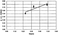
도 2 는 실시예 및 비교예의 시험 기판이 블리딩 폭과 필 강도의 관계를 나타내는 그래프이다.
도 3 은 필 강도와 표면 조도의 관계를 나타내는 도면이다.


Claims (13)
- 금속 기재 표면을 마이크로 에칭제에 의해 에칭하는 에칭 공정과,
에칭된 상기 금속 기재 표면에 표면 처리제를 접촉시켜 금속 기재 표면의 물에 대한 접촉각이 50°이상 150°이하가 되도록 표면 처리하는 표면 처리 공정과,
표면 처리된 금속 기재 표면에 잉크젯 방식으로 수지 조성물의 막을 형성하는 막형성 공정을 구비하는 금속 기재 표면에 수지 조성물의 막이 형성된 막형성 기재를 제조하는 막형성 기재의 제조 방법. - 금속 기재 표면을 마이크로 에칭제에 의해 에칭하는 에칭 공정과,
에칭된 상기 금속 기재 표면에 표면 처리제를 접촉시켜 금속 기재 표면의 솔더 레지스트에 대한 접촉각이 10°이상 120°이하가 되도록 표면 처리하는 표면 처리 공정과,
표면 처리된 금속 기재 표면에 잉크젯 방식으로 수지 조성물의 막을 형성하는 막형성 공정을 구비하는 금속 기재 표면에 수지 조성물의 막이 형성된 막형성 기재를 제조하는 막형성 기재의 제조 방법. - 제 1 항 또는 제 2 항에 있어서,
상기 에칭 공정에 있어서, 금속 기재 표면을 표면 조도 (Ra) 가 0.1 ㎛ 이상 0.8 ㎛ 이하가 되도록 에칭하는 막형성 기재의 제조 방법. - 금속 기재 표면을 기계적으로 조화하는 조화 공정과,
조화된 상기 금속 기재 표면에 표면 처리제를 접촉시켜 금속 기재 표면의 물에 대한 접촉각이 50°이상 150°이하가 되도록 표면 처리하는 표면 처리 공정과,
표면 처리된 금속 기재 표면에 잉크젯 방식으로 수지 조성물의 막을 형성하는 막형성 공정을 구비하는 금속 기재 표면에 수지 조성물의 막이 형성된 막형성 기재를 제조하는 막형성 기재의 제조 방법. - 금속 기재 표면을 기계적으로 조화하는 조화 공정과,
조화된 상기 금속 기재 표면에 표면 처리제를 접촉시켜 금속 기재 표면의 솔더 레지스트에 대한 접촉각이 10°이상 120°이하가 되도록 표면 처리하는 표면 처리 공정과,
표면 처리된 금속 기재 표면에 잉크젯 방식으로 수지 조성물의 막을 형성하는 막형성 공정을 구비하는 금속 기재 표면에 수지 조성물의 막이 형성된 막형성 기재를 제조하는 막형성 기재의 제조 방법. - 제 1 항 내지 제 5 항 중 어느 한 항에 있어서,
상기 표면 처리 공정에 있어서, 알킬기의 탄소수가 6 ∼ 18 인 알킬아민 및 그 염으로 이루어지는 군에서 선택되는 적어도 1 종을 0.001 질량% 이상 1 질량% 이하 함유하는 표면 처리제를 접촉시키는 막형성 기재의 제조 방법. - 제 6 항에 있어서,
알킬기의 탄소수가 6 ∼ 18 인 알킬아민 및 그 염은 헥실아민, 옥타데실아민, 도데실아민, 테트라데실아민 및 옥틸아민으로 이루어지는 군에서 선택되는 적어도 1 종인 막형성 기재의 제조 방법. - 제 1 항 내지 제 7 항 중 어느 한 항에 있어서,
상기 표면 처리제는 pH 4.0 이상 pH 11.5 이하인 막형성 기재의 제조 방법. - 금속 기재 표면의 물에 대한 접촉각이 50°이상 150°이하이고 표면 조도 (Ra) 가 0.1 ㎛ 이상 0.8 ㎛ 이하인 금속 기재 표면에 수지 조성물의 막이 형성된 막형성 기재.
- 금속 기재 표면의 솔더 레지스트에 대한 접촉각이 10°이상 120°이하이고 표면 조도 (Ra) 가 0.1 ㎛ 이상 0.8 ㎛ 이하인 금속 기재 표면에 수지 조성물의 막이 형성된 막형성 기재.
- 알킬기의 탄소수가 6 ∼ 18 인 알킬아민 및 그 염으로 이루어지는 군에서 선택되는 적어도 1 종을 0.001 질량% 이상 1 질량% 이하 함유하는 금속 기재 표면을 처리하기 위한 표면 처리제.
- 제 11 항에 있어서,
알킬기의 탄소수가 6 ∼ 18 인 알킬아민 및 그 염은 헥실아민, 옥타데실아민, 도데실아민, 테트라데실아민 및 옥틸아민으로 이루어지는 군에서 선택되는 적어도 1 종인 표면 처리제. - 제 11 항 또는 제 12 항에 있어서,
상기 표면 처리제는 pH 4.0 이상 pH 11.5 이하인 표면 처리제.
Applications Claiming Priority (3)
| Application Number | Priority Date | Filing Date | Title |
|---|---|---|---|
| JPJP-P-2017-204817 | 2017-10-23 | ||
| JP2017204817 | 2017-10-23 | ||
| PCT/JP2018/038011 WO2019082681A1 (ja) | 2017-10-23 | 2018-10-11 | 膜形成基材の製造方法、膜形成基材及び表面処理剤 |
Publications (2)
| Publication Number | Publication Date |
|---|---|
| KR20200076684A true KR20200076684A (ko) | 2020-06-29 |
| KR102460330B1 KR102460330B1 (ko) | 2022-10-27 |
Family
ID=66246884
Family Applications (1)
| Application Number | Title | Priority Date | Filing Date |
|---|---|---|---|
| KR1020207010911A Active KR102460330B1 (ko) | 2017-10-23 | 2018-10-11 | 막형성 기재의 제조 방법, 막형성 기재 및 표면 처리제 |
Country Status (7)
| Country | Link |
|---|---|
| US (1) | US20200325583A1 (ko) |
| EP (1) | EP3702049A4 (ko) |
| JP (2) | JP6710402B2 (ko) |
| KR (1) | KR102460330B1 (ko) |
| CN (2) | CN111032235B (ko) |
| TW (2) | TWI804194B (ko) |
| WO (1) | WO2019082681A1 (ko) |
Families Citing this family (3)
| Publication number | Priority date | Publication date | Assignee | Title |
|---|---|---|---|---|
| CN111770642A (zh) * | 2020-06-11 | 2020-10-13 | 珠海斗门超毅实业有限公司 | 键合剂在线路板表面处理中的应用方法和线路板 |
| CN114845474B (zh) * | 2022-07-01 | 2022-09-16 | 深圳市板明科技股份有限公司 | 一种pcb喷印图形阻焊方法 |
| JP7634308B1 (ja) | 2024-04-02 | 2025-02-21 | メック株式会社 | 表面処理剤 |
Citations (6)
| Publication number | Priority date | Publication date | Assignee | Title |
|---|---|---|---|---|
| JPH06287774A (ja) * | 1993-04-05 | 1994-10-11 | Metsuku Kk | 銅および銅合金の表面処理剤 |
| JPH0770767A (ja) * | 1993-09-01 | 1995-03-14 | Mitsubishi Gas Chem Co Inc | 銅張積層板用表面処理液および表面処理法 |
| JP2008274311A (ja) * | 2007-04-02 | 2008-11-13 | Mec Kk | 基板の製造方法及びこれに用いる銅表面処理剤 |
| JP2009532205A (ja) * | 2006-04-05 | 2009-09-10 | マクダーミッド インコーポレーテッド | 銅表面にパターンを形成する方法 |
| JP2015192963A (ja) | 2014-03-31 | 2015-11-05 | 太陽インキ製造株式会社 | 塗膜の形成方法 |
| WO2016111036A1 (ja) | 2015-01-07 | 2016-07-14 | 太陽インキ製造株式会社 | 金属基材用表面処理剤 |
Family Cites Families (22)
| Publication number | Priority date | Publication date | Assignee | Title |
|---|---|---|---|---|
| US4895617A (en) * | 1989-05-04 | 1990-01-23 | Olin Corporation | Etchant solution for photoresist-patterned metal layers |
| JPH0847669A (ja) * | 1994-08-05 | 1996-02-20 | Sumitomo Metal Ind Ltd | 耐候性、耐汚れ性に優れた樹脂被覆金属材 |
| JP2000255015A (ja) * | 1999-03-10 | 2000-09-19 | Mitsubishi Polyester Film Copp | ドライフィルムレジスト用カバーフィルム |
| JP2001049458A (ja) * | 1999-08-06 | 2001-02-20 | Furukawa Electric Co Ltd:The | 成形加工性に優れるアルミニウム塗装材の製造方法 |
| EP1330498B1 (de) * | 2000-10-11 | 2006-05-24 | Chemetall GmbH | Verfahren zur beschichtung von metallischen oberflächen mit einer wässerigen zusammensetzung, die wässerige zusammensetzung und verwendung der beschichteten substrate |
| DE60336300D1 (de) * | 2002-01-28 | 2011-04-21 | Jfe Steel Corp | Verfahren zur herstellung einer beschichteten stahlplatte |
| JP2005113228A (ja) * | 2003-10-09 | 2005-04-28 | Daikin Ind Ltd | プレート素材及びその製造方法 |
| JP4467300B2 (ja) * | 2003-12-26 | 2010-05-26 | 株式会社日立製作所 | 配線基板 |
| JP2006118012A (ja) * | 2004-10-22 | 2006-05-11 | Nippon Parkerizing Co Ltd | 金属表面処理剤、金属材料の表面処理方法及び表面処理金属材料 |
| WO2006054888A2 (en) * | 2004-11-16 | 2006-05-26 | Jsr Corporation | Curable liquid composition, cured film, and antistatic laminate |
| CN100544951C (zh) * | 2005-09-21 | 2009-09-30 | 松下电工株式会社 | 防污不锈钢构件 |
| WO2011129032A1 (ja) * | 2010-04-16 | 2011-10-20 | 旭硝子株式会社 | コーティング用組成物およびその製造方法ならびにこれを用いた塗膜の形成方法 |
| CN102259087B (zh) * | 2011-07-20 | 2013-08-07 | 上海电力学院 | 一种具有耐蚀性能的黄铜超疏水表面的制备方法 |
| CN102776548A (zh) * | 2012-06-07 | 2012-11-14 | 清华大学 | 钢材表面超疏水膜层的制备方法 |
| JP6309802B2 (ja) * | 2014-03-26 | 2018-04-11 | 東京応化工業株式会社 | パターン微細化用被覆剤 |
| WO2016010041A1 (ja) * | 2014-07-15 | 2016-01-21 | Jnc株式会社 | 積層体、表面保護物品、積層体の製造方法 |
| US10301580B2 (en) * | 2014-12-30 | 2019-05-28 | Versum Materials Us, Llc | Stripping compositions having high WN/W etching selectivity |
| JP6677448B2 (ja) * | 2015-01-20 | 2020-04-08 | 住友金属鉱山株式会社 | 銅張積層板、及び銅張積層板の製造方法 |
| JP2017034256A (ja) * | 2015-08-05 | 2017-02-09 | 三洋化成工業株式会社 | レジスト基板前処理組成物及びレジスト基板の製造方法 |
| WO2017025949A1 (en) * | 2015-08-13 | 2017-02-16 | Jet Cu Pcb Ltd. | Methods for producing an etch resist pattern on a metallic surface |
| KR102455790B1 (ko) * | 2015-12-22 | 2022-10-19 | 주식회사 이엔에프테크놀로지 | 구리 식각액 조성물 |
| JP6813326B2 (ja) * | 2016-10-06 | 2021-01-13 | 東京応化工業株式会社 | レジストパターンのラフネスを低減させるために用いられる被覆剤、及びラフネスが低減されたレジストパターンの製造方法 |
-
2018
- 2018-10-11 KR KR1020207010911A patent/KR102460330B1/ko active Active
- 2018-10-11 EP EP18871697.1A patent/EP3702049A4/en not_active Withdrawn
- 2018-10-11 WO PCT/JP2018/038011 patent/WO2019082681A1/ja not_active Ceased
- 2018-10-11 CN CN201880051854.9A patent/CN111032235B/zh active Active
- 2018-10-11 CN CN202011142898.8A patent/CN113275229A/zh active Pending
- 2018-10-11 US US16/753,986 patent/US20200325583A1/en not_active Abandoned
- 2018-10-11 JP JP2019550991A patent/JP6710402B2/ja active Active
- 2018-10-22 TW TW111105621A patent/TWI804194B/zh active
- 2018-10-22 TW TW107137197A patent/TWI768139B/zh active
-
2020
- 2020-03-30 JP JP2020060064A patent/JP6986292B2/ja active Active
Patent Citations (7)
| Publication number | Priority date | Publication date | Assignee | Title |
|---|---|---|---|---|
| JPH06287774A (ja) * | 1993-04-05 | 1994-10-11 | Metsuku Kk | 銅および銅合金の表面処理剤 |
| JPH0770767A (ja) * | 1993-09-01 | 1995-03-14 | Mitsubishi Gas Chem Co Inc | 銅張積層板用表面処理液および表面処理法 |
| JP2009532205A (ja) * | 2006-04-05 | 2009-09-10 | マクダーミッド インコーポレーテッド | 銅表面にパターンを形成する方法 |
| JP2008274311A (ja) * | 2007-04-02 | 2008-11-13 | Mec Kk | 基板の製造方法及びこれに用いる銅表面処理剤 |
| JP2015192963A (ja) | 2014-03-31 | 2015-11-05 | 太陽インキ製造株式会社 | 塗膜の形成方法 |
| WO2016111036A1 (ja) | 2015-01-07 | 2016-07-14 | 太陽インキ製造株式会社 | 金属基材用表面処理剤 |
| WO2016111035A1 (ja) | 2015-01-07 | 2016-07-14 | 太陽インキ製造株式会社 | 金属基材用表面処理剤 |
Also Published As
| Publication number | Publication date |
|---|---|
| JPWO2019082681A1 (ja) | 2020-04-16 |
| CN111032235A (zh) | 2020-04-17 |
| EP3702049A1 (en) | 2020-09-02 |
| JP2020124919A (ja) | 2020-08-20 |
| CN111032235B (zh) | 2021-06-22 |
| TWI804194B (zh) | 2023-06-01 |
| EP3702049A4 (en) | 2021-08-11 |
| TW202223152A (zh) | 2022-06-16 |
| US20200325583A1 (en) | 2020-10-15 |
| KR102460330B1 (ko) | 2022-10-27 |
| TW201928117A (zh) | 2019-07-16 |
| TWI768139B (zh) | 2022-06-21 |
| JP6710402B2 (ja) | 2020-06-17 |
| JP6986292B2 (ja) | 2021-12-22 |
| CN113275229A (zh) | 2021-08-20 |
| WO2019082681A1 (ja) | 2019-05-02 |
Similar Documents
| Publication | Publication Date | Title |
|---|---|---|
| KR102502531B1 (ko) | 환원 처리와 동시에 사용되는 무전해 도금용 전처리액, 및 프린트 배선 기판의 제조 방법 | |
| JP6986292B2 (ja) | 膜形成基材 | |
| KR20090115094A (ko) | 무전해 금도금조 및 방법 | |
| KR102440121B1 (ko) | 프린트 배선 기판의 제조 방법 | |
| US6783690B2 (en) | Method of stripping silver from a printed circuit board | |
| JP2008231459A (ja) | ポリイミド樹脂上への導電性皮膜の形成方法 | |
| KR20130075729A (ko) | 구리 및 구리 합금의 마이크로 에칭을 위한 조성물 및 방법 | |
| US7666471B2 (en) | Polyimide substrate and method of manufacturing printed wiring board using the same | |
| JP6281686B2 (ja) | メタルマスクとその製造方法 | |
| JP3051683B2 (ja) | 無電解金めっき方法 | |
| JP2012025974A (ja) | 無電解金めっき液及び無電解金めっき方法 | |
| CN108476611A (zh) | 印刷电路表面抛光、使用方法和由此制成的组件 | |
| KR101719180B1 (ko) | 무전해 팔라듐 도금 또는 무전해 팔라듐 합금 도금의 전처리용 활성화액 | |
| JP7634308B1 (ja) | 表面処理剤 | |
| JP2006219736A (ja) | 表面処理Al板 | |
| KR20090009734A (ko) | 표면처리제 | |
| EP1973670A1 (en) | Method of using ultrasonics to plate silver | |
| JP5775684B2 (ja) | 導電性金属紋様形成方法及び電子電気素子 | |
| TW201931030A (zh) | 抗蝕劑之剝離液 | |
| JP2001247973A (ja) | 洗浄・調整剤及びプリント配線板の無電解銅めっき方法 | |
| CN112867811A (zh) | 表面处理液和含镍材料的表面处理方法 | |
| JP2010236025A (ja) | 無電解めっき用前処理剤及びこれを用いた無電解めっき方法 |
Legal Events
| Date | Code | Title | Description |
|---|---|---|---|
| PA0105 | International application |
Patent event date: 20200414 Patent event code: PA01051R01D Comment text: International Patent Application |
|
| PG1501 | Laying open of application | ||
| A201 | Request for examination | ||
| A302 | Request for accelerated examination | ||
| AMND | Amendment | ||
| PA0201 | Request for examination |
Patent event code: PA02012R01D Patent event date: 20211007 Comment text: Request for Examination of Application |
|
| PA0302 | Request for accelerated examination |
Patent event date: 20211007 Patent event code: PA03022R01D Comment text: Request for Accelerated Examination |
|
| E902 | Notification of reason for refusal | ||
| PE0902 | Notice of grounds for rejection |
Comment text: Notification of reason for refusal Patent event date: 20220114 Patent event code: PE09021S01D |
|
| AMND | Amendment | ||
| E601 | Decision to refuse application | ||
| PE0601 | Decision on rejection of patent |
Patent event date: 20220530 Comment text: Decision to Refuse Application Patent event code: PE06012S01D Patent event date: 20220114 Comment text: Notification of reason for refusal Patent event code: PE06011S01I |
|
| X091 | Application refused [patent] | ||
| AMND | Amendment | ||
| PX0901 | Re-examination |
Patent event code: PX09011S01I Patent event date: 20220530 Comment text: Decision to Refuse Application Patent event code: PX09012R01I Patent event date: 20220228 Comment text: Amendment to Specification, etc. Patent event code: PX09012R01I Patent event date: 20211007 Comment text: Amendment to Specification, etc. |
|
| PX0701 | Decision of registration after re-examination |
Patent event date: 20220926 Comment text: Decision to Grant Registration Patent event code: PX07013S01D Patent event date: 20220826 Comment text: Amendment to Specification, etc. Patent event code: PX07012R01I Patent event date: 20220530 Comment text: Decision to Refuse Application Patent event code: PX07011S01I Patent event date: 20220228 Comment text: Amendment to Specification, etc. Patent event code: PX07012R01I Patent event date: 20211007 Comment text: Amendment to Specification, etc. Patent event code: PX07012R01I |
|
| X701 | Decision to grant (after re-examination) | ||
| GRNT | Written decision to grant | ||
| PR0701 | Registration of establishment |
Comment text: Registration of Establishment Patent event date: 20221025 Patent event code: PR07011E01D |
|
| PR1002 | Payment of registration fee |
Payment date: 20221025 End annual number: 3 Start annual number: 1 |
|
| PG1601 | Publication of registration |