KR20200077047A - 백금 검지체 센서의 고온 환경 안정화 공정 방법 - Google Patents
백금 검지체 센서의 고온 환경 안정화 공정 방법 Download PDFInfo
- Publication number
- KR20200077047A KR20200077047A KR1020180166184A KR20180166184A KR20200077047A KR 20200077047 A KR20200077047 A KR 20200077047A KR 1020180166184 A KR1020180166184 A KR 1020180166184A KR 20180166184 A KR20180166184 A KR 20180166184A KR 20200077047 A KR20200077047 A KR 20200077047A
- Authority
- KR
- South Korea
- Prior art keywords
- adhesive layer
- layer
- high temperature
- detection
- platinum
- Prior art date
- Legal status (The legal status is an assumption and is not a legal conclusion. Google has not performed a legal analysis and makes no representation as to the accuracy of the status listed.)
- Granted
Links
Images


Classifications
-
- G—PHYSICS
- G01—MEASURING; TESTING
- G01N—INVESTIGATING OR ANALYSING MATERIALS BY DETERMINING THEIR CHEMICAL OR PHYSICAL PROPERTIES
- G01N27/00—Investigating or analysing materials by the use of electric, electrochemical, or magnetic means
- G01N27/02—Investigating or analysing materials by the use of electric, electrochemical, or magnetic means by investigating impedance
- G01N27/04—Investigating or analysing materials by the use of electric, electrochemical, or magnetic means by investigating impedance by investigating resistance
-
- C—CHEMISTRY; METALLURGY
- C23—COATING METALLIC MATERIAL; COATING MATERIAL WITH METALLIC MATERIAL; CHEMICAL SURFACE TREATMENT; DIFFUSION TREATMENT OF METALLIC MATERIAL; COATING BY VACUUM EVAPORATION, BY SPUTTERING, BY ION IMPLANTATION OR BY CHEMICAL VAPOUR DEPOSITION, IN GENERAL; INHIBITING CORROSION OF METALLIC MATERIAL OR INCRUSTATION IN GENERAL
- C23C—COATING METALLIC MATERIAL; COATING MATERIAL WITH METALLIC MATERIAL; SURFACE TREATMENT OF METALLIC MATERIAL BY DIFFUSION INTO THE SURFACE, BY CHEMICAL CONVERSION OR SUBSTITUTION; COATING BY VACUUM EVAPORATION, BY SPUTTERING, BY ION IMPLANTATION OR BY CHEMICAL VAPOUR DEPOSITION, IN GENERAL
- C23C14/00—Coating by vacuum evaporation, by sputtering or by ion implantation of the coating forming material
- C23C14/02—Pretreatment of the material to be coated
- C23C14/024—Deposition of sublayers, e.g. to promote adhesion of the coating
-
- C—CHEMISTRY; METALLURGY
- C23—COATING METALLIC MATERIAL; COATING MATERIAL WITH METALLIC MATERIAL; CHEMICAL SURFACE TREATMENT; DIFFUSION TREATMENT OF METALLIC MATERIAL; COATING BY VACUUM EVAPORATION, BY SPUTTERING, BY ION IMPLANTATION OR BY CHEMICAL VAPOUR DEPOSITION, IN GENERAL; INHIBITING CORROSION OF METALLIC MATERIAL OR INCRUSTATION IN GENERAL
- C23C—COATING METALLIC MATERIAL; COATING MATERIAL WITH METALLIC MATERIAL; SURFACE TREATMENT OF METALLIC MATERIAL BY DIFFUSION INTO THE SURFACE, BY CHEMICAL CONVERSION OR SUBSTITUTION; COATING BY VACUUM EVAPORATION, BY SPUTTERING, BY ION IMPLANTATION OR BY CHEMICAL VAPOUR DEPOSITION, IN GENERAL
- C23C14/00—Coating by vacuum evaporation, by sputtering or by ion implantation of the coating forming material
- C23C14/06—Coating by vacuum evaporation, by sputtering or by ion implantation of the coating forming material characterised by the coating material
- C23C14/14—Metallic material, boron or silicon
Landscapes
- Chemical & Material Sciences (AREA)
- Chemical Kinetics & Catalysis (AREA)
- Engineering & Computer Science (AREA)
- Materials Engineering (AREA)
- Mechanical Engineering (AREA)
- Metallurgy (AREA)
- Organic Chemistry (AREA)
- Electrochemistry (AREA)
- Physics & Mathematics (AREA)
- Health & Medical Sciences (AREA)
- Life Sciences & Earth Sciences (AREA)
- Analytical Chemistry (AREA)
- Biochemistry (AREA)
- General Health & Medical Sciences (AREA)
- General Physics & Mathematics (AREA)
- Immunology (AREA)
- Pathology (AREA)
- Thermistors And Varistors (AREA)
- Investigating Or Analyzing Materials By The Use Of Fluid Adsorption Or Reactions (AREA)
Abstract
Description
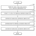
도 2는 본 발명의 일실시예의 백금 검지체 센서의 고온 환경 안정화 공정 방법의 절차도이고,
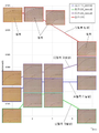
도 3 내지 도 4는 도 2의 백금 검지체 센서의 고온 환경 안정화 공정 방법을 따라 제작된 실시예들과 종래 제작 방법에 의해 제작된 비교예의 어닐링 시간별 저항 변화를 나타낸 그래프이다.
| 구분 | 공정조건 | 비고 |
| A | Ti 15nm 증착, 섭씨 700도 가열 후 1시간 유지, Pt 250nm 증착 |
|
| B | Ti 20nm 증착,섭씨 700도 가열 후 1시간 유지, Pt 250nm 증착 |
|
| C | Ti 25nm 증착,섭씨 700도 가열 후 1시간 유지, Pt 250nm 증착 |
|
| D | Ti 20nm 증착,Pt 250nm 증착 | 비교용 시편 |
| 구분 | Pt 증착후 가열 | 1시간 추가 | 2시간 추가 | 3시간 추가 | |
| A | 0.661Ω | 0.549Ω | 0.554Ω | 0.554Ω | 0.554Ω |
| B | 0.665Ω | 0.540Ω | 0.549Ω | 0.549Ω | 0.540Ω |
| C | 0.651Ω | 0.554Ω | 0.558Ω | 0.558Ω | 0.563Ω |
| D | 0.670Ω | 0.582Ω | 0.582Ω | 0.577Ω | 0.567Ω |
S100: 접착레이어 형성 단계
S110: 접착레이어 열처리 단계
S120: 검지레이어 형성 단계
S130: 검지레이어 열처리 단계
Claims (6)
- 기판에 Ti, Ta 또는 Cr이 증착되는 접착레이어 형성 단계;
상기 접착레이어가 열처리되는 접착레이어 열처리 단계;
상기 접착레이어에 Pt가 증착되는 검지레이어 형성 단계를 포함하는 백금 검지체 센서의 고온 환경 안정화 공정 방법.
- 제1항에 있어서,
상기 접착레이어 형성 단계 수행 전에,
상기 기판에 PE-TEOS, SiO2, SiXNX 중 어느 하나가 증착되는 절연층 형성 단계가 수행되는 백금 검지체 센서의 고온 환경 안정화 공정 방법.
- 제1항에 있어서,
상기 검지레이어 형성 단계에서,
목표로 하는 상기 검지레이어 두께의 30% 내지 70% 두께가 되도록 상기 Ti, Ta 또는 Cr가 상기 기판에 증착되는 백금 검지체 센서의 고온 환경 안정화 공정 방법.
- 제1항에 있어서,
상기 접착레이어 열처리 단계에서 상기 접착레이어는 섭씨 600도 내지 섭씨 800도의 공기 또는 산소분위기에 30분 내지 4시간 노출되고,
상기 접착레이어를 이루는 Ti는 TiO2, Ta는 TaO2, Cr은 CrO2로 변이되는 백금 검지체 센서의 고온 환경 안정화 공정 방법.
- 제1항에 있어서,
상기 검지레이어가 열처리되는 검지레이어 열처리 단계를 더 포함하고,
상기 검지레이어 열처리 단계는,
상기 검지레이어를 섭씨 600도 내지 섭씨 800도의 공기 또는 질소분위기에 1시간 이상 노출시키는 백금 검지체 센서의 고온 환경 안정화 공정 방법.
- 청구항 1 내지 청구항 5 중 어느 하나의 백금 검지체 센서의 고온 환경 안정화 공정 방법을 통해 제작된 백금 검지체 센서.
Priority Applications (1)
| Application Number | Priority Date | Filing Date | Title |
|---|---|---|---|
| KR1020180166184A KR102170210B1 (ko) | 2018-12-20 | 2018-12-20 | 백금 검지체 센서의 고온 환경 안정화 공정 방법 |
Applications Claiming Priority (1)
| Application Number | Priority Date | Filing Date | Title |
|---|---|---|---|
| KR1020180166184A KR102170210B1 (ko) | 2018-12-20 | 2018-12-20 | 백금 검지체 센서의 고온 환경 안정화 공정 방법 |
Publications (2)
| Publication Number | Publication Date |
|---|---|
| KR20200077047A true KR20200077047A (ko) | 2020-06-30 |
| KR102170210B1 KR102170210B1 (ko) | 2020-10-28 |
Family
ID=71121000
Family Applications (1)
| Application Number | Title | Priority Date | Filing Date |
|---|---|---|---|
| KR1020180166184A Active KR102170210B1 (ko) | 2018-12-20 | 2018-12-20 | 백금 검지체 센서의 고온 환경 안정화 공정 방법 |
Country Status (1)
| Country | Link |
|---|---|
| KR (1) | KR102170210B1 (ko) |
Cited By (1)
| Publication number | Priority date | Publication date | Assignee | Title |
|---|---|---|---|---|
| CN115058686A (zh) * | 2022-06-17 | 2022-09-16 | 广东风华高新科技股份有限公司 | 一种调控Pt膜层晶体生长取向的制备方法 |
Citations (6)
| Publication number | Priority date | Publication date | Assignee | Title |
|---|---|---|---|---|
| JPS62284216A (ja) * | 1986-06-02 | 1987-12-10 | Nippon Soken Inc | 流量センサ用膜式抵抗の製造方法 |
| JPH02226017A (ja) * | 1988-12-23 | 1990-09-07 | Honeywell Inc | 薄膜白金素子用接着層を有するセンサ構造 |
| JPH1183781A (ja) * | 1997-09-11 | 1999-03-26 | Fuji Electric Co Ltd | ガスセンサ用触媒の製造方法 |
| JPH11211687A (ja) * | 1998-01-20 | 1999-08-06 | Toyota Central Res & Dev Lab Inc | 窒素酸化物検知素子の製造方法 |
| KR20060026149A (ko) * | 2004-09-20 | 2006-03-23 | 대양전기공업 주식회사 | 크롬산화막층을 갖는 백금전극저항체 및 그 제조방법 |
| KR20150124078A (ko) | 2014-04-25 | 2015-11-05 | (주) 래트론 | 온도 센서 소자 및 그 제조 방법 |
-
2018
- 2018-12-20 KR KR1020180166184A patent/KR102170210B1/ko active Active
Patent Citations (6)
| Publication number | Priority date | Publication date | Assignee | Title |
|---|---|---|---|---|
| JPS62284216A (ja) * | 1986-06-02 | 1987-12-10 | Nippon Soken Inc | 流量センサ用膜式抵抗の製造方法 |
| JPH02226017A (ja) * | 1988-12-23 | 1990-09-07 | Honeywell Inc | 薄膜白金素子用接着層を有するセンサ構造 |
| JPH1183781A (ja) * | 1997-09-11 | 1999-03-26 | Fuji Electric Co Ltd | ガスセンサ用触媒の製造方法 |
| JPH11211687A (ja) * | 1998-01-20 | 1999-08-06 | Toyota Central Res & Dev Lab Inc | 窒素酸化物検知素子の製造方法 |
| KR20060026149A (ko) * | 2004-09-20 | 2006-03-23 | 대양전기공업 주식회사 | 크롬산화막층을 갖는 백금전극저항체 및 그 제조방법 |
| KR20150124078A (ko) | 2014-04-25 | 2015-11-05 | (주) 래트론 | 온도 센서 소자 및 그 제조 방법 |
Cited By (2)
| Publication number | Priority date | Publication date | Assignee | Title |
|---|---|---|---|---|
| CN115058686A (zh) * | 2022-06-17 | 2022-09-16 | 广东风华高新科技股份有限公司 | 一种调控Pt膜层晶体生长取向的制备方法 |
| CN115058686B (zh) * | 2022-06-17 | 2024-02-20 | 广东风华高新科技股份有限公司 | 一种调控Pt膜层晶体生长取向的制备方法 |
Also Published As
| Publication number | Publication date |
|---|---|
| KR102170210B1 (ko) | 2020-10-28 |
Similar Documents
| Publication | Publication Date | Title |
|---|---|---|
| US7963171B2 (en) | High temperature strain gages | |
| KR101024801B1 (ko) | 온도 측정 부재, 온도 측정 장치 및 온도 측정 방법 | |
| JPH06300649A (ja) | 薄膜歪抵抗材料とその製造方法及び薄膜歪みセンサ | |
| US8502639B1 (en) | Nanocomposite semiconducting material with reduced resistivity | |
| Ababneh et al. | Electrical and morphological characterization of platinum thin-films with various adhesion layers for high temperature applications | |
| Lin et al. | The impact of thermal annealing on the temperature dependent resistance behavior of Pt thin films sputtered on Si and Al2O3 substrates | |
| JP2009036756A (ja) | 温度測定方法、温度測定具および温度測定装置 | |
| KR20200077047A (ko) | 백금 검지체 센서의 고온 환경 안정화 공정 방법 | |
| Kreider et al. | Thin-film resistance thermometers on silicon wafers | |
| Gregory et al. | Piezoresistive properties of ITO strain sensors prepared with controlled nanoporosity | |
| JP2019192740A (ja) | 歪抵抗膜および歪センサ、ならびにそれらの製造方法 | |
| CN117848200A (zh) | 应变电阻膜及物理量传感器及应变电阻膜的制造方法 | |
| US5902504A (en) | Systems and methods for determining semiconductor wafer temperature and calibrating a vapor deposition device | |
| Chung et al. | RTD characteristics for micro-thermal sensors | |
| JP7103600B2 (ja) | 歪センサ、およびその製造方法 | |
| Yeung et al. | Micro-pressure sensors made of indium tin oxide thin films | |
| JP4802013B2 (ja) | 温度センサおよびその製造方法 | |
| KR100629651B1 (ko) | 크롬산화막층을 갖는 백금전극저항체 및 그 제조방법 | |
| TW200605101A (en) | Thermistor thin-film and its forming method | |
| Veselov et al. | Modification properties of the dielectric membrane films using high temperature annealing | |
| Kattelus et al. | Amorphous Mo–N and Mo–Si–N films in microelectromechanical systems | |
| JP2020524290A (ja) | シート抵抗及び薄膜センサ | |
| Madsen et al. | Titanium nitride as a strain gauge material | |
| Park et al. | Effects of excess PbO and Zr/Ti ratio on microstructure and electrical properties of PZT films | |
| KR100395246B1 (ko) | 마이크로 열센서용 측온저항체형 온도센서 및 그 제조방법 |
Legal Events
| Date | Code | Title | Description |
|---|---|---|---|
| PA0109 | Patent application |
Patent event code: PA01091R01D Comment text: Patent Application Patent event date: 20181220 |
|
| PA0201 | Request for examination | ||
| PE0902 | Notice of grounds for rejection |
Comment text: Notification of reason for refusal Patent event date: 20200318 Patent event code: PE09021S01D |
|
| PG1501 | Laying open of application | ||
| E701 | Decision to grant or registration of patent right | ||
| PE0701 | Decision of registration |
Patent event code: PE07011S01D Comment text: Decision to Grant Registration Patent event date: 20201019 |
|
| GRNT | Written decision to grant | ||
| PR0701 | Registration of establishment |
Comment text: Registration of Establishment Patent event date: 20201020 Patent event code: PR07011E01D |
|
| PR1002 | Payment of registration fee |
Payment date: 20201021 End annual number: 3 Start annual number: 1 |
|
| PG1601 | Publication of registration | ||
| PR1001 | Payment of annual fee |
Payment date: 20240919 Start annual number: 5 End annual number: 5 |