KR20200077342A - 광 경로 제어 부재 및 이를 포함하는 표시 장치 - Google Patents
광 경로 제어 부재 및 이를 포함하는 표시 장치 Download PDFInfo
- Publication number
- KR20200077342A KR20200077342A KR1020180166750A KR20180166750A KR20200077342A KR 20200077342 A KR20200077342 A KR 20200077342A KR 1020180166750 A KR1020180166750 A KR 1020180166750A KR 20180166750 A KR20180166750 A KR 20180166750A KR 20200077342 A KR20200077342 A KR 20200077342A
- Authority
- KR
- South Korea
- Prior art keywords
- pattern
- pattern portion
- control member
- path control
- light
- Prior art date
- Legal status (The legal status is an assumption and is not a legal conclusion. Google has not performed a legal analysis and makes no representation as to the accuracy of the status listed.)
- Withdrawn
Links
- 230000003287 optical effect Effects 0.000 claims abstract description 60
- 239000000758 substrate Substances 0.000 claims abstract description 52
- 229920005989 resin Polymers 0.000 claims abstract description 51
- 239000011347 resin Substances 0.000 claims abstract description 51
- 238000000034 method Methods 0.000 claims description 7
- 239000010410 layer Substances 0.000 description 49
- 239000011295 pitch Substances 0.000 description 41
- 230000000052 comparative effect Effects 0.000 description 23
- 241000220259 Raphanus Species 0.000 description 16
- 235000006140 Raphanus sativus var sativus Nutrition 0.000 description 16
- 239000010408 film Substances 0.000 description 15
- 230000000694 effects Effects 0.000 description 12
- 238000002834 transmittance Methods 0.000 description 12
- 239000012790 adhesive layer Substances 0.000 description 11
- 239000000463 material Substances 0.000 description 7
- 239000010409 thin film Substances 0.000 description 7
- 230000007423 decrease Effects 0.000 description 6
- 239000004973 liquid crystal related substance Substances 0.000 description 6
- 239000011241 protective layer Substances 0.000 description 6
- 230000000903 blocking effect Effects 0.000 description 5
- 239000002346 layers by function Substances 0.000 description 5
- 230000004048 modification Effects 0.000 description 4
- 238000012986 modification Methods 0.000 description 4
- -1 acryl Chemical group 0.000 description 3
- 239000000853 adhesive Substances 0.000 description 3
- 230000001070 adhesive effect Effects 0.000 description 3
- 239000011159 matrix material Substances 0.000 description 3
- 230000001681 protective effect Effects 0.000 description 3
- LPZOCVVDSHQFST-UHFFFAOYSA-N 2-[4-[2-(2,3-dihydro-1H-inden-2-ylamino)pyrimidin-5-yl]-3-ethylpyrazol-1-yl]-1-(2,4,6,7-tetrahydrotriazolo[4,5-c]pyridin-5-yl)ethanone Chemical compound C1C(CC2=CC=CC=C12)NC1=NC=C(C=N1)C=1C(=NN(C=1)CC(=O)N1CC2=C(CC1)NN=N2)CC LPZOCVVDSHQFST-UHFFFAOYSA-N 0.000 description 2
- 230000005540 biological transmission Effects 0.000 description 2
- 239000003738 black carbon Substances 0.000 description 2
- 239000004033 plastic Substances 0.000 description 2
- 229920003023 plastic Polymers 0.000 description 2
- 229920000139 polyethylene terephthalate Polymers 0.000 description 2
- 239000005020 polyethylene terephthalate Substances 0.000 description 2
- 230000003667 anti-reflective effect Effects 0.000 description 1
- 239000011324 bead Substances 0.000 description 1
- 230000008878 coupling Effects 0.000 description 1
- 238000010168 coupling process Methods 0.000 description 1
- 238000005859 coupling reaction Methods 0.000 description 1
- 230000007547 defect Effects 0.000 description 1
- 230000002542 deteriorative effect Effects 0.000 description 1
- 239000006185 dispersion Substances 0.000 description 1
- 238000005538 encapsulation Methods 0.000 description 1
- 238000005516 engineering process Methods 0.000 description 1
- 150000002148 esters Chemical class 0.000 description 1
- 238000005530 etching Methods 0.000 description 1
- 239000005357 flat glass Substances 0.000 description 1
- 230000004313 glare Effects 0.000 description 1
- 239000012535 impurity Substances 0.000 description 1
- 230000001788 irregular Effects 0.000 description 1
- 238000004519 manufacturing process Methods 0.000 description 1
- 238000005259 measurement Methods 0.000 description 1
- 125000002496 methyl group Chemical group [H]C([H])([H])* 0.000 description 1
- 230000035515 penetration Effects 0.000 description 1
- 239000004417 polycarbonate Substances 0.000 description 1
- 229920000515 polycarbonate Polymers 0.000 description 1
- 238000007650 screen-printing Methods 0.000 description 1
- 238000007789 sealing Methods 0.000 description 1
- 238000010186 staining Methods 0.000 description 1
- 238000006467 substitution reaction Methods 0.000 description 1
- 229920001187 thermosetting polymer Polymers 0.000 description 1
- 239000012780 transparent material Substances 0.000 description 1
Images







Classifications
-
- G—PHYSICS
- G02—OPTICS
- G02B—OPTICAL ELEMENTS, SYSTEMS OR APPARATUS
- G02B26/00—Optical devices or arrangements for the control of light using movable or deformable optical elements
- G02B26/08—Optical devices or arrangements for the control of light using movable or deformable optical elements for controlling the direction of light
Landscapes
- Physics & Mathematics (AREA)
- General Physics & Mathematics (AREA)
- Optics & Photonics (AREA)
- Devices For Indicating Variable Information By Combining Individual Elements (AREA)
- Planar Illumination Modules (AREA)
- Liquid Crystal (AREA)
Abstract
Description
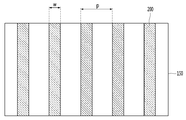
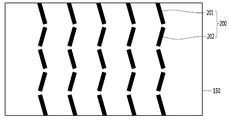
도 2는 실시예에 따른 광 경로 제어 부재의 상면도를 도시한 도면이다.
도 3은 도 2의 A-A' 영역의 단면도에서 패턴부가 배치되지 않은 단면도를 도시한 도면이다.
도 4는 도 2의 A-A' 영역을 절단한 단면도를 도시한 도면이다.
도 5는 실시예에 따른 광 경로 제어 부재의 패턴을 설명하기 위한 상면도를 도시한 도면이다.
도 6은 실시예 및 비교예에 따른 광 경로 제어 부재의 무아레 현상을 설명하기 위한 그래프이다.
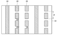
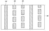
도 7 내지 도 12는 다른 실시예에 따른 광 경로 제어 부재의 상면도를 도시한 도면이다.
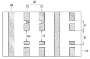
도 13 내지 도 15는 또 다른 실시예에 따른 광 경로 제어 부재의 상면도를 도시한 도면이다.
도 16은 실시예들에 따른 광 경로 제어 부재가 적용되는 표시 장치의 단면도를 도시한 도면이다.
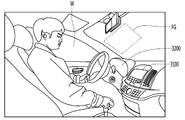
도 17은 실시예에 따른 광 경로 제어 부재가 적용되는 디스플레이 장치의 일 실시예를 설명하기 위한 도면들이다.

| 광경로제어부재의 패턴부수(k) | 표시패널의 화소패턴수(m) | |
| 계열1 | 1 | 4 |
| 계열2 | 1 | 3 |
| 계열3 | 1 | 3 |
| 계열4 | 1 | 3 |
| 계열5 | 1 | 4 |
| 계열6 | 1 | 4 |
| 계열7 | 3 | 4 |
| 계열8 | 1 | 3 |
| 계열9 | 2 | 4 |
| 계열10 | 1 | 4 |
| 계열11 | 2 | 3 |
| 계열12 | 2 | 4 |
| 계열13 | 3 | 4 |
| 계열14 | 2 | 3 |
| 계열15 | 1 | 3 |
| 계열16 | 2 | 4 |
| 광경로제어부재의 패턴부수(k) | 패턴부 피치ㅣ(㎛) | 표시패널의 화소패턴수(m) | 표시패널의 패턴 피치(㎛) | 결합파장(λ) | 무아레 발생여부 | |
| 실시예1 | 1 | 15 | 4 | 141 | 26 | 무 |
| 실시예2 | 1 | 16 | 3 | 141 | 24 | 무 |
| 실시예3 | 1 | 17 | 3 | 138 | 27 | 무 |
| 실시예4 | 1 | 18 | 3 | 138 | 30 | 무 |
| 실시예5 | 1 | 19 | 4 | 135 | 43 | 무 |
| 실시예6 | 1 | 20 | 4 | 135 | 49 | 무 |
| 실시예7 | 3 | 21 | 4 | 135 | 9 | 무 |
| 실시예8 | 1 | 22 | 3 | 132 | 44 | 무 |
| 실시예9 | 2 | 23 | 4 | 132 | 18 | 무 |
| 실시예10 | 1 | 24 | 4 | 129 | 94 | 무 |
| 실시예11 | 2 | 25 | 3 | 129 | 18 | 무 |
| 실시예12 | 2 | 26 | 4 | 129 | 22 | 무 |
| 실시예13 | 3 | 27 | 4 | 126 | 13 | 무 |
| 실시예14 | 2 | 28 | 3 | 126 | 21 | 무 |
| 실시예15 | 1 | 29 | 3 | 123 | 99 | 무 |
| 실시예16 | 2 | 30 | 4 | 123 | 29 | 무 |
| 비교예1 | 1 | 35 | 4 | 141 | 4.935 | 유 |
| 비교예2 | 1 | 46.5 | 3 | 141 | 4.371 | 유 |
| 비교예3 | 1 | 45 | 3 | 138 | 2.070 | 유 |
| 비교예4 | 1 | 45.5 | 3 | 138 | 4.186 | 유 |
| 비교예5 | 1 | 33.5 | 4 | 135 | 4.523 | 유 |
| 비교예6 | 1 | 34 | 4 | 135 | 4.590 | 유 |
| 비교예7 | 3 | 102 | 4 | 135 | 4.590 | 유 |
| 비교예8 | 1 | 44.5 | 3 | 132 | 3.916 | 유 |
| 비교예9 | 2 | 65.5 | 4 | 132 | 4.323 | 유 |
| 비교예10 | 1 | 32 | 4 | 129 | 4.128 | 유 |
| 비교예11 | 2 | 85 | 3 | 129 | 3.655 | 유 |
| 비교예12 | 2 | 65 | 4 | 129 | 4.193 | 유 |
| 비교예13 | 3 | 94 | 4 | 126 | 5.922 | 유 |
| 비교예14 | 2 | 85 | 3 | 126 | 3.570 | 유 |
| 비교예15 | 1 | 41.5 | 3 | 123 | 3.403 | 유 |
| 비교예16 | 2 | 60.5 | 4 | 123 | 1.860 | 유 |
Claims (10)
- 베이스 기재;
상기 베이스 기재 상에 배치되고, 서로 이격하는 복수의 음각부를 포함하는 수지층; 및
상기 복수의 음각부 내부에 배치되고, 서로 이격하는 복수의 패턴부를 포함하고,
상기 복수의 패턴부들의 피치(pitch)는 30㎛ 이하인 광 경로 제어 부재. - 제 1항에 있어서,
상기 패턴부는 제 1 패턴부 및 제 2 패턴부를 포함하고,
상기 제 1 패턴부와 상기 제 2 패턴부는 다른 형상으로 형성되는 광 경로 제어 부재. - 제 2항에 있어서,
상기 제 2 패턴부는 복수의 단락부를 포함하는 광 경로 제어 부재 - 제 4항에 있어서,
상기 단락부의 폭은 1㎛ 내지 50㎛인 광 경로 제어 부재. - 제 4항에 있어서,
각각의 단락부의 폭은 랜덤하게 형성되는 광 경로 제어 부재. - 제 1항에 있어서,
상기 패턴부는 제 1 방향으로 연장하는 제 1 서브 패턴부; 및 상기 제 1 방향과 다른 방향인 제 2 방향으로 연장하는 제 2 서브 패턴부를 포함하는 광 경로 제어 부재. - 제 3항에 있어서,
상기 제 1 패턴부 및 상기 제 2 패턴부를 포함하는 전체 패턴부에 대한 상기 제 2 패턴부의 비율은 상기 제 1 패턴부의 비율보다 큰 광 경로 제어 부재. - 표시 패널; 및
상기 표시 패널 상에 배치되는 광 경로 제어 부재를 포함하고,
상기 광 경로 제어 부재는,
상기 표시 패널 상에 배치되고, 서로 이격하는 복수의 음각부 및 상기 복수의 양각부를 포함하는 수지층;
상기 복수의 음각부 내부에 배치되고, 서로 이격하는 복수의 패턴부; 및
상기 수지층 상에 배치되는 베이스 기재를 포함하고,
상기 복수의 패턴부들의 피치는 30㎛ 이하이고,
상기 화소 패턴의 피치는 120㎛ 내지 145㎛인 표시 장치. - 제 7항에 있어서,
상기 표시 장치는 하기 수식으로 정의되는 결합 파장 값(λ)이 2500㎛ 미만이 표시 장치.
[수식]

(P1은 광 경로 제어 부재의 패턴부의 피치이고, P2는 표시 패널와 화소 패턴의 피치이고, k는 광 경로 제어 부재의 패턴부의 수이고, m은 표시 패널와 화소 패턴의 수이다.) - 제 1항에 있어서,
상기 패턴부는 제 1 패턴부 및 제 2 패턴부를 포함하고,
상기 제 2 패턴부는 복수의 단락부를 포함하는 표시 장치.
Priority Applications (3)
| Application Number | Priority Date | Filing Date | Title |
|---|---|---|---|
| KR1020180166750A KR20200077342A (ko) | 2018-12-20 | 2018-12-20 | 광 경로 제어 부재 및 이를 포함하는 표시 장치 |
| PCT/KR2019/008307 WO2020013533A1 (ko) | 2018-07-12 | 2019-07-05 | 광 경로 제어 부재 및 이를 포함하는 표시 장치 |
| US17/258,838 US20210271095A1 (en) | 2018-07-12 | 2019-07-05 | Optical path control member and display device comprising same |
Applications Claiming Priority (1)
| Application Number | Priority Date | Filing Date | Title |
|---|---|---|---|
| KR1020180166750A KR20200077342A (ko) | 2018-12-20 | 2018-12-20 | 광 경로 제어 부재 및 이를 포함하는 표시 장치 |
Publications (1)
| Publication Number | Publication Date |
|---|---|
| KR20200077342A true KR20200077342A (ko) | 2020-06-30 |
Family
ID=71120975
Family Applications (1)
| Application Number | Title | Priority Date | Filing Date |
|---|---|---|---|
| KR1020180166750A Withdrawn KR20200077342A (ko) | 2018-07-12 | 2018-12-20 | 광 경로 제어 부재 및 이를 포함하는 표시 장치 |
Country Status (1)
| Country | Link |
|---|---|
| KR (1) | KR20200077342A (ko) |
Cited By (1)
| Publication number | Priority date | Publication date | Assignee | Title |
|---|---|---|---|---|
| WO2022045661A1 (ko) * | 2020-08-25 | 2022-03-03 | 엘지이노텍 주식회사 | 광 경로 제어 부재 및 이를 포함하는 디스플레이 장치 |
-
2018
- 2018-12-20 KR KR1020180166750A patent/KR20200077342A/ko not_active Withdrawn
Cited By (2)
| Publication number | Priority date | Publication date | Assignee | Title |
|---|---|---|---|---|
| WO2022045661A1 (ko) * | 2020-08-25 | 2022-03-03 | 엘지이노텍 주식회사 | 광 경로 제어 부재 및 이를 포함하는 디스플레이 장치 |
| US12419177B2 (en) | 2020-08-25 | 2025-09-16 | Lg Innotek Co., Ltd. | Optical path control member and display device comprising same |
Similar Documents
| Publication | Publication Date | Title |
|---|---|---|
| KR102404740B1 (ko) | 광 제어 부재 및 이를 포함하는 디스플레이 장치 | |
| KR102404742B1 (ko) | 광 제어 부재 및 이를 포함하는 표시 장치 | |
| EP2354835A1 (en) | Liquid crystal display with protective front face plate | |
| CN113997868B (zh) | 车载显示装置 | |
| KR102568862B1 (ko) | 광 경로 제어 부재 및 이를 포함하는 표시 장치 | |
| KR102766599B1 (ko) | 광 경로 제어 부재 및 이를 포함하는 디스플레이 장치 | |
| KR102774371B1 (ko) | 광 경로 제어 부재 및 이를 포함하는 표시 장치 | |
| KR102766613B1 (ko) | 광 경로 제어 부재 및 이를 포함하는 디스플레이 장치 | |
| KR102644111B1 (ko) | 광 경로 제어 부재 및 이를 포함하는 표시 장치 | |
| KR102481663B1 (ko) | 차광 부재 및 이를 포함하는 디스플레이 장치 | |
| KR20200077342A (ko) | 광 경로 제어 부재 및 이를 포함하는 표시 장치 | |
| KR102774380B1 (ko) | 광 경로 제어 부재 및 이를 포함하는 디스플레이 장치 | |
| KR20200019535A (ko) | 광 경로 제어 부재 및 이를 포함하는 표시 장치 | |
| KR102809715B1 (ko) | 광 경로 제어 부재 및 이를 포함하는 표시 장치 | |
| US20210271096A1 (en) | Optical path control member and display device comprising same | |
| US12353089B2 (en) | Light route control member and display having the same | |
| KR102756139B1 (ko) | 광 경로 제어 부재 및 이를 포함하는 디스플레이 장치 | |
| KR102552883B1 (ko) | 광 경로 제어 부재 및 이를 포함하는 표시 장치 | |
| KR102774377B1 (ko) | 광 경로 제어 부재 및 이를 포함하는 디스플레이 장치 | |
| KR102608110B1 (ko) | 광 경로 제어 부재 및 이를 포함하는 표시 장치 | |
| US20210271095A1 (en) | Optical path control member and display device comprising same | |
| KR102774381B1 (ko) | 광 경로 제어 부재 및 이를 포함하는 디스플레이 장치 | |
| KR20200017801A (ko) | 광 경로 제어 부재 및 이를 포함하는 표시 장치 | |
| KR102872801B1 (ko) | 광 경로 제어 부재 및 이를 포함하는 디스플레이 장치 | |
| KR102756134B1 (ko) | 광 경로 제어 부재 및 이를 포함하는 디스플레이 장치 |
Legal Events
| Date | Code | Title | Description |
|---|---|---|---|
| PA0109 | Patent application |
Patent event code: PA01091R01D Comment text: Patent Application Patent event date: 20181220 |
|
| PG1501 | Laying open of application | ||
| A201 | Request for examination | ||
| PA0201 | Request for examination |
Patent event code: PA02012R01D Patent event date: 20210908 Comment text: Request for Examination of Application Patent event code: PA02011R01I Patent event date: 20181220 Comment text: Patent Application |
|
| E902 | Notification of reason for refusal | ||
| PE0902 | Notice of grounds for rejection |
Comment text: Notification of reason for refusal Patent event date: 20231018 Patent event code: PE09021S01D |
|
| PC1202 | Submission of document of withdrawal before decision of registration |
Comment text: [Withdrawal of Procedure relating to Patent, etc.] Withdrawal (Abandonment) Patent event code: PC12021R01D Patent event date: 20231020 |
|
| WITB | Written withdrawal of application |