KR20200077477A - 표시 장치 - Google Patents
표시 장치 Download PDFInfo
- Publication number
- KR20200077477A KR20200077477A KR1020200074109A KR20200074109A KR20200077477A KR 20200077477 A KR20200077477 A KR 20200077477A KR 1020200074109 A KR1020200074109 A KR 1020200074109A KR 20200074109 A KR20200074109 A KR 20200074109A KR 20200077477 A KR20200077477 A KR 20200077477A
- Authority
- KR
- South Korea
- Prior art keywords
- layer
- disposed
- electrode
- source
- semiconductor layer
- Prior art date
- Legal status (The legal status is an assumption and is not a legal conclusion. Google has not performed a legal analysis and makes no representation as to the accuracy of the status listed.)
- Ceased
Links
Images









Classifications
-
- H—ELECTRICITY
- H10—SEMICONDUCTOR DEVICES; ELECTRIC SOLID-STATE DEVICES NOT OTHERWISE PROVIDED FOR
- H10K—ORGANIC ELECTRIC SOLID-STATE DEVICES
- H10K59/00—Integrated devices, or assemblies of multiple devices, comprising at least one organic light-emitting element covered by group H10K50/00
- H10K59/10—OLED displays
- H10K59/12—Active-matrix OLED [AMOLED] displays
- H10K59/121—Active-matrix OLED [AMOLED] displays characterised by the geometry or disposition of pixel elements
- H10K59/1213—Active-matrix OLED [AMOLED] displays characterised by the geometry or disposition of pixel elements the pixel elements being TFTs
-
- H01L27/3262—
-
- H01L27/3248—
-
- H01L27/3258—
-
- H01L27/3265—
-
- H—ELECTRICITY
- H10—SEMICONDUCTOR DEVICES; ELECTRIC SOLID-STATE DEVICES NOT OTHERWISE PROVIDED FOR
- H10K—ORGANIC ELECTRIC SOLID-STATE DEVICES
- H10K50/00—Organic light-emitting devices
- H10K50/10—OLEDs or polymer light-emitting diodes [PLED]
- H10K50/11—OLEDs or polymer light-emitting diodes [PLED] characterised by the electroluminescent [EL] layers
- H10K50/125—OLEDs or polymer light-emitting diodes [PLED] characterised by the electroluminescent [EL] layers specially adapted for multicolour light emission, e.g. for emitting white light
- H10K50/13—OLEDs or polymer light-emitting diodes [PLED] characterised by the electroluminescent [EL] layers specially adapted for multicolour light emission, e.g. for emitting white light comprising stacked EL layers within one EL unit
-
- H—ELECTRICITY
- H10—SEMICONDUCTOR DEVICES; ELECTRIC SOLID-STATE DEVICES NOT OTHERWISE PROVIDED FOR
- H10K—ORGANIC ELECTRIC SOLID-STATE DEVICES
- H10K50/00—Organic light-emitting devices
- H10K50/80—Constructional details
- H10K50/805—Electrodes
- H10K50/81—Anodes
-
- H—ELECTRICITY
- H10—SEMICONDUCTOR DEVICES; ELECTRIC SOLID-STATE DEVICES NOT OTHERWISE PROVIDED FOR
- H10K—ORGANIC ELECTRIC SOLID-STATE DEVICES
- H10K50/00—Organic light-emitting devices
- H10K50/80—Constructional details
- H10K50/805—Electrodes
- H10K50/82—Cathodes
-
- H—ELECTRICITY
- H10—SEMICONDUCTOR DEVICES; ELECTRIC SOLID-STATE DEVICES NOT OTHERWISE PROVIDED FOR
- H10K—ORGANIC ELECTRIC SOLID-STATE DEVICES
- H10K59/00—Integrated devices, or assemblies of multiple devices, comprising at least one organic light-emitting element covered by group H10K50/00
- H10K59/10—OLED displays
- H10K59/12—Active-matrix OLED [AMOLED] displays
- H10K59/121—Active-matrix OLED [AMOLED] displays characterised by the geometry or disposition of pixel elements
- H10K59/1216—Active-matrix OLED [AMOLED] displays characterised by the geometry or disposition of pixel elements the pixel elements being capacitors
-
- H—ELECTRICITY
- H10—SEMICONDUCTOR DEVICES; ELECTRIC SOLID-STATE DEVICES NOT OTHERWISE PROVIDED FOR
- H10K—ORGANIC ELECTRIC SOLID-STATE DEVICES
- H10K59/00—Integrated devices, or assemblies of multiple devices, comprising at least one organic light-emitting element covered by group H10K50/00
- H10K59/10—OLED displays
- H10K59/12—Active-matrix OLED [AMOLED] displays
- H10K59/122—Pixel-defining structures or layers, e.g. banks
-
- H—ELECTRICITY
- H10—SEMICONDUCTOR DEVICES; ELECTRIC SOLID-STATE DEVICES NOT OTHERWISE PROVIDED FOR
- H10K—ORGANIC ELECTRIC SOLID-STATE DEVICES
- H10K59/00—Integrated devices, or assemblies of multiple devices, comprising at least one organic light-emitting element covered by group H10K50/00
- H10K59/10—OLED displays
- H10K59/12—Active-matrix OLED [AMOLED] displays
- H10K59/123—Connection of the pixel electrodes to the thin film transistors [TFT]
-
- H—ELECTRICITY
- H10—SEMICONDUCTOR DEVICES; ELECTRIC SOLID-STATE DEVICES NOT OTHERWISE PROVIDED FOR
- H10K—ORGANIC ELECTRIC SOLID-STATE DEVICES
- H10K59/00—Integrated devices, or assemblies of multiple devices, comprising at least one organic light-emitting element covered by group H10K50/00
- H10K59/10—OLED displays
- H10K59/12—Active-matrix OLED [AMOLED] displays
- H10K59/124—Insulating layers formed between TFT elements and OLED elements
-
- H—ELECTRICITY
- H10—SEMICONDUCTOR DEVICES; ELECTRIC SOLID-STATE DEVICES NOT OTHERWISE PROVIDED FOR
- H10K—ORGANIC ELECTRIC SOLID-STATE DEVICES
- H10K59/00—Integrated devices, or assemblies of multiple devices, comprising at least one organic light-emitting element covered by group H10K50/00
- H10K59/10—OLED displays
- H10K59/12—Active-matrix OLED [AMOLED] displays
- H10K59/126—Shielding, e.g. light-blocking means over the TFTs
-
- H—ELECTRICITY
- H10—SEMICONDUCTOR DEVICES; ELECTRIC SOLID-STATE DEVICES NOT OTHERWISE PROVIDED FOR
- H10K—ORGANIC ELECTRIC SOLID-STATE DEVICES
- H10K59/00—Integrated devices, or assemblies of multiple devices, comprising at least one organic light-emitting element covered by group H10K50/00
- H10K59/10—OLED displays
- H10K59/12—Active-matrix OLED [AMOLED] displays
- H10K59/131—Interconnections, e.g. wiring lines or terminals
-
- H—ELECTRICITY
- H10—SEMICONDUCTOR DEVICES; ELECTRIC SOLID-STATE DEVICES NOT OTHERWISE PROVIDED FOR
- H10K—ORGANIC ELECTRIC SOLID-STATE DEVICES
- H10K59/00—Integrated devices, or assemblies of multiple devices, comprising at least one organic light-emitting element covered by group H10K50/00
- H10K59/30—Devices specially adapted for multicolour light emission
- H10K59/38—Devices specially adapted for multicolour light emission comprising colour filters or colour changing media [CCM]
-
- H—ELECTRICITY
- H10—SEMICONDUCTOR DEVICES; ELECTRIC SOLID-STATE DEVICES NOT OTHERWISE PROVIDED FOR
- H10K—ORGANIC ELECTRIC SOLID-STATE DEVICES
- H10K77/00—Constructional details of devices covered by this subclass and not covered by groups H10K10/80, H10K30/80, H10K50/80 or H10K59/80
- H10K77/10—Substrates, e.g. flexible substrates
- H10K77/111—Flexible substrates
-
- H—ELECTRICITY
- H10—SEMICONDUCTOR DEVICES; ELECTRIC SOLID-STATE DEVICES NOT OTHERWISE PROVIDED FOR
- H10K—ORGANIC ELECTRIC SOLID-STATE DEVICES
- H10K2102/00—Constructional details relating to the organic devices covered by this subclass
- H10K2102/301—Details of OLEDs
- H10K2102/311—Flexible OLED
-
- Y—GENERAL TAGGING OF NEW TECHNOLOGICAL DEVELOPMENTS; GENERAL TAGGING OF CROSS-SECTIONAL TECHNOLOGIES SPANNING OVER SEVERAL SECTIONS OF THE IPC; TECHNICAL SUBJECTS COVERED BY FORMER USPC CROSS-REFERENCE ART COLLECTIONS [XRACs] AND DIGESTS
- Y02—TECHNOLOGIES OR APPLICATIONS FOR MITIGATION OR ADAPTATION AGAINST CLIMATE CHANGE
- Y02E—REDUCTION OF GREENHOUSE GAS [GHG] EMISSIONS, RELATED TO ENERGY GENERATION, TRANSMISSION OR DISTRIBUTION
- Y02E10/00—Energy generation through renewable energy sources
- Y02E10/50—Photovoltaic [PV] energy
- Y02E10/549—Organic PV cells
Landscapes
- Engineering & Computer Science (AREA)
- Microelectronics & Electronic Packaging (AREA)
- Physics & Mathematics (AREA)
- Optics & Photonics (AREA)
- Geometry (AREA)
- Devices For Indicating Variable Information By Combining Individual Elements (AREA)
- Vehicle Body Suspensions (AREA)
- Diaphragms For Electromechanical Transducers (AREA)
- Measuring Pulse, Heart Rate, Blood Pressure Or Blood Flow (AREA)
- Electroluminescent Light Sources (AREA)
- Chemical & Material Sciences (AREA)
- Crystallography & Structural Chemistry (AREA)
Abstract
Description
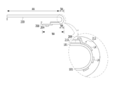
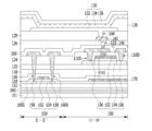
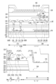
도 2는 도 1에서 선"I-I'"를 따라 절취한 표시 장치를 나타내는 단면도이다.
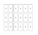
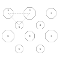
도 3a 및 도 3b는 도 1에 도시된 액티브 영역에 배치되는 서브 화소들을 나타내는 평면도이다.
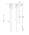
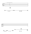
도 4a 및 도 4b는 도 1에 도시된 벤딩 영역에 배치되는 신호 링크의 실시예들을 나타내는 평면도이다.
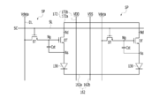
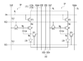
도 5a 및 도 5b는 도 1에 도시된 표시 장치의 각 서브 화소를 설명하기 위한 회로도들이다.
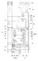
도 6은 도 5b에 도시된 서브 화소를 나타내는 평면도이다.
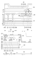
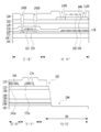
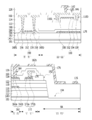
도 7은 도 6에서 선 Ⅱ-Ⅱ', Ⅲ-Ⅲ', Ⅳ-Ⅳ', Ⅴ-Ⅴ', Ⅵ-Ⅵ'를 따라 절취한 유기 발광 표시 장치를 나타내는 단면도이다.
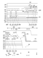
도 8a 내지 도 8c는 도 7에 도시된 스토리지 커패시터의 다른 실시예들을 나타내는 단면도들이다.
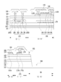
도 9a 및 도 9b는 도 7에 도시된 벤딩 영역의 다른 실시예들을 나타내는 단면도들이다.
도 10a 내지 도 10m은 도 7에 도시된 유기 발광 표시 장치의 제조 방법을 설명하기 위한 단면도들이다.
106,156 : 소스 전극 108,110 : 드레인 전극
130 : 발광 소자 154 : 다결정 반도체층
162 : 저전위 공급 라인 172 : 고전위 공급 라인
176, LK : 신호 링크 180 : 스토리지 커패시터
192,194 : 개구
Claims (18)
- 액티브 영역과 벤딩 영역을 가지는 기판과;
상기 액티브 영역에 배치되며, 제1 반도체층, 제1 게이트 전극, 제1 소스 전극 및 제1 드레인 전극을 가지는 제1 박막트랜지스터와;
상기 액티브 영역에 배치되며, 제2 반도체층, 제2 게이트 전극, 제2 소스 전극 및 제2 드레인 전극을 가지는 제2 박막트랜지스터와;
상기 제1 소스 및 제1 드레인 전극과, 제2 소스 및 제2 드레인 전극 상에 배치되는 보호막;
제1 박막트랜지스터와 상기 제2 박막트랜지스터 상에 배치되는 발광 소자와;
상기 액티브 영역에 배치되는 다수의 절연층과;
상기 벤딩 영역에 배치되는 상기 다수의 절연층의 측면을 노출시키는 적어도 하나의 개구부를 가지는 표시장치. - 제 1 항에 있어서,
상기 다수의 절연층은 상기 제1 게이트 전극과 상기 제1 반도체층 사이에 배치되는 하부 게이트 절연층과;
상기 제1 게이트 전극과 상기 제2 반도체층 사이에 배치되는 하부 층간절연층 및 상부 버퍼층과;
상기 제2 반도체층과 상기 제2 소스 전극 및 제2 드레인 전극 사이에 배치되는 상부 층간 절연층을 포함하는 표시장치. - 제 1 항에 있어서,
상기 제1 소스 및 제1 드레인 전극과, 제2 소스 및 제2 드레인 전극 상에 배치되는 보호막을 더 구비하며,
상기 다수의 절연층은
상기 다결정 반도체층과 상기 하부 층간 절연층 사이에 배치되는 하부 게이트 절연층을 더 포함하는 표시 장치. - 제 2 항에 있어서,
상기 제2 반도체층과 중첩되며, 상기 하부 게이트 절연층 및 상기 상부 버퍼층을 사이에 두고 상기 제2 게이트 전극과 중첩되는 차광층을 더 구비하는 표시장치. - 제 4 항에 있어서,
상기 제2 게이트 전극은 상기 제2 소스 전극과 상기 상부 층간 절연층을 사이에 두고 중첩되어 제1 스토리지 커패시터를 이루며, 상기 제2 게이트 전극은 상기 차광층과 제2 스토리지 커패시터를 이루며,
상기 제1 및 제2 스토리지 커패시터는 병렬로 접속되는 표시장치. - 제 2 항에 있어서,
상기 액티브 영역에 배치되는 다수의 컨택홀과;
상기 다수의 컨택홀은
상기 제1 소스 및 제1 드레인 전극 각각과 상기 제1 반도체층 사이에 배치되는 상기 하부 층간 절연층 및 상기 상부 버퍼층과 상기 상부 층간 절연층을 포함하는 다수의 절연층을 관통하여, 상기 제1 반도체층을 노출시키는 제1 소스 및 제1 드레인 컨택홀과;
상기 상부 층간 절연층을 관통하여 상기 제2 반도체층을 노출시키는 제2 소스 및 제2 드레인 컨택홀을 구비하는 표시장치. - 제 2 항에 있어서,
상기 기판 상에 배치되는 멀티 버퍼층과;
상기 멀티 버퍼층 상에 배치되는 하부 버퍼층을 더 구비하며,
상기 개구부는 상기 벤딩 영역에 배치되는 상기 멀티 버퍼층, 상기 하부 버퍼층, 상기 하부 게이트 절연층, 상기 하부 층간 절연층 및 상기 상부 버퍼층을 관통하여,
상기 벤딩 영역의 기판은 상기 개구부에 의해 노출되는 표시장치. - 제 7 항에 있어서,
상기 발광소자와 상기 제1 내지 제2 박막트랜지스터 사이에 배치되는 평탄화층이 상기 개구부를 채우며,
상기 벤딩 영역의 기판은 상기 액티브 영역의 기판보다 두께가 얇은 표시장치. - 제 1 항에 있어서,
상기 제1 및 제2 소스 전극은 상기 제1 및 제2 드레인 전극과 동일 평면인 상기 상부 층간 절연막 상에, 상기 제1 및 제2 드레인 전극과 동일 재질로 이루어진 표시 장치. - 제 1 항에 있어서,
상기 발광 소자는 애노드 전극과 캐소드 전극을 더 포함하고,
상기 캐소드 전극과 접속되는 저전위 공급라인과;
상기 저전위 공급라인과 인접하게 배치되는 고전위 공급 라인을 더 구비하여,
상기 저전위 공급 라인 및 상기 고전위 공급 라인 중 적어도 어느 하나는 메쉬 형태로 배치되는 표시 장치. - 제 1 항에 있어서,
상기 적어도 하나의 개구부는 상기 다수의 절연층의 측면을 계단 형태로 노출시키는 표시 장치. - 제 1 항에 있어서,
상기 적어도 하나의 개구부는 서로 수직하게 중첩되는 제1 및 제2 개구부를 구비하는 표시 장치. - 제 12 항에 있어서,
상기 제2 개구부는 상기 다수의 절연층 중 상기 제1 반도체층 하부에 배치되는 제1 절연층의 제1 측면을 노출시키며,
상기 제1 개구부는 상기 다수의 절연층 중 상기 제2 반도체층 상에 배치되는 제2 절연층의 제2 측면을 노출시키는 표시 장치. - 제 13 항에 있어서,
상기 제2 개구부에 의해 노출된 제1 측면은 상기 제2 측면보다 돌출되는 표시 장치. - 제 1 항에 있어서,
상기 제1 및 제2 박막트랜지스터와 상기 발광 소자 사이에 배치되는 평탄화층을 더 구비하는 표시 장치. - 제 15 항에 있어서,
상기 개구부는 상기 기판의 내측면을 노출시키며,
상기 평탄화층은 상기 기판의 내측면 상에 배치되는 표시 장치. - 제 15 항에 있어서,
상기 평탄화층 상에 배치되는 신호 링크를 더 구비하는 표시 장치. - 제 1 항에 있어서,
상기 다수의 절연층 상에서, 상기 개구부에 의해 노출된 상기 다수의 절연층의 측면을 따라 배치되는 신호 링크를 더 구비하는 표시 장치.
Priority Applications (4)
| Application Number | Priority Date | Filing Date | Title |
|---|---|---|---|
| KR1020200074109A KR20200077477A (ko) | 2020-06-18 | 2020-06-18 | 표시 장치 |
| KR1020210082519A KR102438783B1 (ko) | 2020-06-18 | 2021-06-24 | 표시 장치 |
| KR1020220106901A KR102769214B1 (ko) | 2020-06-18 | 2022-08-25 | 표시 장치 |
| KR1020250013852A KR20250024785A (ko) | 2020-06-18 | 2025-02-04 | 표시 장치 |
Applications Claiming Priority (1)
| Application Number | Priority Date | Filing Date | Title |
|---|---|---|---|
| KR1020200074109A KR20200077477A (ko) | 2020-06-18 | 2020-06-18 | 표시 장치 |
Related Parent Applications (1)
| Application Number | Title | Priority Date | Filing Date |
|---|---|---|---|
| KR1020170175054A Division KR102126552B1 (ko) | 2017-12-19 | 2017-12-19 | 표시 장치 |
Related Child Applications (1)
| Application Number | Title | Priority Date | Filing Date |
|---|---|---|---|
| KR1020210082519A Division KR102438783B1 (ko) | 2020-06-18 | 2021-06-24 | 표시 장치 |
Publications (1)
| Publication Number | Publication Date |
|---|---|
| KR20200077477A true KR20200077477A (ko) | 2020-06-30 |
Family
ID=71121390
Family Applications (4)
| Application Number | Title | Priority Date | Filing Date |
|---|---|---|---|
| KR1020200074109A Ceased KR20200077477A (ko) | 2020-06-18 | 2020-06-18 | 표시 장치 |
| KR1020210082519A Active KR102438783B1 (ko) | 2020-06-18 | 2021-06-24 | 표시 장치 |
| KR1020220106901A Active KR102769214B1 (ko) | 2020-06-18 | 2022-08-25 | 표시 장치 |
| KR1020250013852A Pending KR20250024785A (ko) | 2020-06-18 | 2025-02-04 | 표시 장치 |
Family Applications After (3)
| Application Number | Title | Priority Date | Filing Date |
|---|---|---|---|
| KR1020210082519A Active KR102438783B1 (ko) | 2020-06-18 | 2021-06-24 | 표시 장치 |
| KR1020220106901A Active KR102769214B1 (ko) | 2020-06-18 | 2022-08-25 | 표시 장치 |
| KR1020250013852A Pending KR20250024785A (ko) | 2020-06-18 | 2025-02-04 | 표시 장치 |
Country Status (1)
| Country | Link |
|---|---|
| KR (4) | KR20200077477A (ko) |
Cited By (5)
| Publication number | Priority date | Publication date | Assignee | Title |
|---|---|---|---|---|
| KR20220096489A (ko) * | 2020-12-31 | 2022-07-07 | 엘지디스플레이 주식회사 | 표시 장치 |
| US12058889B2 (en) | 2020-11-24 | 2024-08-06 | Samsung Display Co., Ltd. | Display device |
| US12245462B2 (en) | 2020-12-21 | 2025-03-04 | Samsung Display Co., Ltd. | Display device |
| US12490599B2 (en) | 2021-02-23 | 2025-12-02 | Samsung Display Co., Ltd. | Display panel and display apparatus including the same |
| US12514065B2 (en) * | 2021-12-14 | 2025-12-30 | Lg Display Co., Ltd. | Organic light-emitting display apparatus comprising a storage capacitor having three storage capacitor electrodes |
Family Cites Families (16)
| Publication number | Priority date | Publication date | Assignee | Title |
|---|---|---|---|---|
| KR102397873B1 (ko) * | 2014-02-24 | 2022-05-16 | 엘지디스플레이 주식회사 | 표시장치 |
| KR102251176B1 (ko) * | 2014-02-24 | 2021-05-11 | 엘지디스플레이 주식회사 | 박막 트랜지스터 기판 및 이를 이용한 표시장치 |
| KR102180067B1 (ko) * | 2014-08-07 | 2020-11-17 | 엘지디스플레이 주식회사 | 박막트랜지스터 어레이 기판 |
| KR102467574B1 (ko) * | 2014-08-29 | 2022-11-18 | 엘지디스플레이 주식회사 | 박막 트랜지스터 기판 및 이를 이용한 표시장치 |
| US9543370B2 (en) * | 2014-09-24 | 2017-01-10 | Apple Inc. | Silicon and semiconducting oxide thin-film transistor displays |
| US9356087B1 (en) * | 2014-12-10 | 2016-05-31 | Lg Display Co., Ltd. | Flexible display device with bridged wire traces |
| KR102405257B1 (ko) * | 2015-01-28 | 2022-06-03 | 삼성디스플레이 주식회사 | 표시 장치 |
| KR102381285B1 (ko) * | 2015-08-06 | 2022-03-31 | 삼성디스플레이 주식회사 | 가요성 표시 장치 및 이의 제조 방법 |
| KR102455318B1 (ko) * | 2015-10-30 | 2022-10-18 | 삼성디스플레이 주식회사 | 유기 발광 표시 장치 |
| KR102424108B1 (ko) * | 2015-11-26 | 2022-07-25 | 엘지디스플레이 주식회사 | 박막 트랜지스터 기판 및 이를 이용한 표시장치 |
| KR102611499B1 (ko) * | 2015-12-15 | 2023-12-06 | 엘지디스플레이 주식회사 | 플렉서블 표시장치 |
| KR102387791B1 (ko) * | 2015-12-31 | 2022-04-15 | 엘지디스플레이 주식회사 | 유기전계 발광표시장치 및 그 제조방법 |
| KR102495844B1 (ko) * | 2016-02-12 | 2023-02-07 | 삼성디스플레이 주식회사 | 디스플레이 장치 |
| JP6756508B2 (ja) * | 2016-04-04 | 2020-09-16 | 株式会社ジャパンディスプレイ | 表示装置 |
| KR102587229B1 (ko) * | 2016-04-22 | 2023-10-12 | 삼성디스플레이 주식회사 | 표시 장치 |
| KR102729661B1 (ko) * | 2016-09-22 | 2024-11-13 | 삼성디스플레이 주식회사 | 표시 장치 및 그 제조 방법 |
-
2020
- 2020-06-18 KR KR1020200074109A patent/KR20200077477A/ko not_active Ceased
-
2021
- 2021-06-24 KR KR1020210082519A patent/KR102438783B1/ko active Active
-
2022
- 2022-08-25 KR KR1020220106901A patent/KR102769214B1/ko active Active
-
2025
- 2025-02-04 KR KR1020250013852A patent/KR20250024785A/ko active Pending
Cited By (5)
| Publication number | Priority date | Publication date | Assignee | Title |
|---|---|---|---|---|
| US12058889B2 (en) | 2020-11-24 | 2024-08-06 | Samsung Display Co., Ltd. | Display device |
| US12245462B2 (en) | 2020-12-21 | 2025-03-04 | Samsung Display Co., Ltd. | Display device |
| KR20220096489A (ko) * | 2020-12-31 | 2022-07-07 | 엘지디스플레이 주식회사 | 표시 장치 |
| US12490599B2 (en) | 2021-02-23 | 2025-12-02 | Samsung Display Co., Ltd. | Display panel and display apparatus including the same |
| US12514065B2 (en) * | 2021-12-14 | 2025-12-30 | Lg Display Co., Ltd. | Organic light-emitting display apparatus comprising a storage capacitor having three storage capacitor electrodes |
Also Published As
| Publication number | Publication date |
|---|---|
| KR20220124124A (ko) | 2022-09-13 |
| KR102769214B1 (ko) | 2025-02-21 |
| KR102438783B1 (ko) | 2022-08-31 |
| KR20210083226A (ko) | 2021-07-06 |
| KR20250024785A (ko) | 2025-02-19 |
Similar Documents
| Publication | Publication Date | Title |
|---|---|---|
| JP7478784B2 (ja) | 表示装置 | |
| JP7511723B2 (ja) | 表示装置 | |
| US12453181B2 (en) | Display device | |
| KR102104981B1 (ko) | 표시 장치 | |
| JP7105847B2 (ja) | 表示装置 | |
| KR102769214B1 (ko) | 표시 장치 | |
| KR102367823B1 (ko) | 표시 장치 | |
| KR102501143B1 (ko) | 표시 장치의 제조방법 | |
| KR102414597B1 (ko) | 표시 장치 |
Legal Events
| Date | Code | Title | Description |
|---|---|---|---|
| A107 | Divisional application of patent | ||
| PA0107 | Divisional application |
Comment text: Divisional Application of Patent Patent event date: 20200618 Patent event code: PA01071R01D Filing date: 20171219 Application number text: 1020170175054 |
|
| PA0201 | Request for examination | ||
| PG1501 | Laying open of application | ||
| E902 | Notification of reason for refusal | ||
| PE0902 | Notice of grounds for rejection |
Comment text: Notification of reason for refusal Patent event date: 20200915 Patent event code: PE09021S01D |
|
| AMND | Amendment | ||
| E601 | Decision to refuse application | ||
| PE0601 | Decision on rejection of patent |
Patent event date: 20210330 Comment text: Decision to Refuse Application Patent event code: PE06012S01D Patent event date: 20200915 Comment text: Notification of reason for refusal Patent event code: PE06011S01I |
|
| X091 | Application refused [patent] | ||
| PX0901 | Re-examination |
Patent event code: PX09011S01I Patent event date: 20210330 Comment text: Decision to Refuse Application Patent event code: PX09012R01I Patent event date: 20201109 Comment text: Amendment to Specification, etc. |
|
| E601 | Decision to refuse application | ||
| E801 | Decision on dismissal of amendment | ||
| PE0601 | Decision on rejection of patent |
Patent event date: 20210527 Comment text: Decision to Refuse Application Patent event code: PE06012S01D Patent event date: 20200915 Comment text: Notification of reason for refusal Patent event code: PE06011S01I |
|
| PE0801 | Dismissal of amendment |
Patent event code: PE08012E01D Comment text: Decision on Dismissal of Amendment Patent event date: 20210527 Patent event code: PE08011R01I Comment text: Amendment to Specification, etc. Patent event date: 20210426 Patent event code: PE08011R01I Comment text: Amendment to Specification, etc. Patent event date: 20201109 |