KR20200078480A - Solid state imaging element, manufacturing method and electronic device - Google Patents
Solid state imaging element, manufacturing method and electronic device Download PDFInfo
- Publication number
- KR20200078480A KR20200078480A KR1020207007640A KR20207007640A KR20200078480A KR 20200078480 A KR20200078480 A KR 20200078480A KR 1020207007640 A KR1020207007640 A KR 1020207007640A KR 20207007640 A KR20207007640 A KR 20207007640A KR 20200078480 A KR20200078480 A KR 20200078480A
- Authority
- KR
- South Korea
- Prior art keywords
- substrate
- electrode
- solid
- state imaging
- light
- Prior art date
- Legal status (The legal status is an assumption and is not a legal conclusion. Google has not performed a legal analysis and makes no representation as to the accuracy of the status listed.)
- Granted
Links
Images






Classifications
-
- H—ELECTRICITY
- H10—SEMICONDUCTOR DEVICES; ELECTRIC SOLID-STATE DEVICES NOT OTHERWISE PROVIDED FOR
- H10F—INORGANIC SEMICONDUCTOR DEVICES SENSITIVE TO INFRARED RADIATION, LIGHT, ELECTROMAGNETIC RADIATION OF SHORTER WAVELENGTH OR CORPUSCULAR RADIATION
- H10F39/00—Integrated devices, or assemblies of multiple devices, comprising at least one element covered by group H10F30/00, e.g. radiation detectors comprising photodiode arrays
- H10F39/80—Constructional details of image sensors
- H10F39/809—Constructional details of image sensors of hybrid image sensors
-
- H01L27/14634—
-
- H01L21/76898—
-
- H01L23/5226—
-
- H01L27/14623—
-
- H01L27/14636—
-
- H—ELECTRICITY
- H04—ELECTRIC COMMUNICATION TECHNIQUE
- H04N—PICTORIAL COMMUNICATION, e.g. TELEVISION
- H04N25/00—Circuitry of solid-state image sensors [SSIS]; Control thereof
- H04N25/70—SSIS architectures; Circuits associated therewith
- H04N25/76—Addressed sensors, e.g. MOS or CMOS sensors
-
- H04N5/374—
-
- H—ELECTRICITY
- H10—SEMICONDUCTOR DEVICES; ELECTRIC SOLID-STATE DEVICES NOT OTHERWISE PROVIDED FOR
- H10F—INORGANIC SEMICONDUCTOR DEVICES SENSITIVE TO INFRARED RADIATION, LIGHT, ELECTROMAGNETIC RADIATION OF SHORTER WAVELENGTH OR CORPUSCULAR RADIATION
- H10F39/00—Integrated devices, or assemblies of multiple devices, comprising at least one element covered by group H10F30/00, e.g. radiation detectors comprising photodiode arrays
- H10F39/80—Constructional details of image sensors
- H10F39/802—Geometry or disposition of elements in pixels, e.g. address-lines or gate electrodes
-
- H—ELECTRICITY
- H10—SEMICONDUCTOR DEVICES; ELECTRIC SOLID-STATE DEVICES NOT OTHERWISE PROVIDED FOR
- H10F—INORGANIC SEMICONDUCTOR DEVICES SENSITIVE TO INFRARED RADIATION, LIGHT, ELECTROMAGNETIC RADIATION OF SHORTER WAVELENGTH OR CORPUSCULAR RADIATION
- H10F39/00—Integrated devices, or assemblies of multiple devices, comprising at least one element covered by group H10F30/00, e.g. radiation detectors comprising photodiode arrays
- H10F39/80—Constructional details of image sensors
- H10F39/805—Coatings
- H10F39/8057—Optical shielding
-
- H—ELECTRICITY
- H10—SEMICONDUCTOR DEVICES; ELECTRIC SOLID-STATE DEVICES NOT OTHERWISE PROVIDED FOR
- H10F—INORGANIC SEMICONDUCTOR DEVICES SENSITIVE TO INFRARED RADIATION, LIGHT, ELECTROMAGNETIC RADIATION OF SHORTER WAVELENGTH OR CORPUSCULAR RADIATION
- H10F39/00—Integrated devices, or assemblies of multiple devices, comprising at least one element covered by group H10F30/00, e.g. radiation detectors comprising photodiode arrays
- H10F39/80—Constructional details of image sensors
- H10F39/806—Optical elements or arrangements associated with the image sensors
- H10F39/8063—Microlenses
-
- H—ELECTRICITY
- H10—SEMICONDUCTOR DEVICES; ELECTRIC SOLID-STATE DEVICES NOT OTHERWISE PROVIDED FOR
- H10F—INORGANIC SEMICONDUCTOR DEVICES SENSITIVE TO INFRARED RADIATION, LIGHT, ELECTROMAGNETIC RADIATION OF SHORTER WAVELENGTH OR CORPUSCULAR RADIATION
- H10F39/00—Integrated devices, or assemblies of multiple devices, comprising at least one element covered by group H10F30/00, e.g. radiation detectors comprising photodiode arrays
- H10F39/80—Constructional details of image sensors
- H10F39/811—Interconnections
-
- H—ELECTRICITY
- H10—SEMICONDUCTOR DEVICES; ELECTRIC SOLID-STATE DEVICES NOT OTHERWISE PROVIDED FOR
- H10P—GENERIC PROCESSES OR APPARATUS FOR THE MANUFACTURE OR TREATMENT OF DEVICES COVERED BY CLASS H10
- H10P14/00—Formation of materials, e.g. in the shape of layers or pillars
- H10P14/40—Formation of materials, e.g. in the shape of layers or pillars of conductive or resistive materials
-
- H—ELECTRICITY
- H10—SEMICONDUCTOR DEVICES; ELECTRIC SOLID-STATE DEVICES NOT OTHERWISE PROVIDED FOR
- H10W—GENERIC PACKAGES, INTERCONNECTIONS, CONNECTORS OR OTHER CONSTRUCTIONAL DETAILS OF DEVICES COVERED BY CLASS H10
- H10W20/00—Interconnections in chips, wafers or substrates
- H10W20/01—Manufacture or treatment
-
- H—ELECTRICITY
- H10—SEMICONDUCTOR DEVICES; ELECTRIC SOLID-STATE DEVICES NOT OTHERWISE PROVIDED FOR
- H10W—GENERIC PACKAGES, INTERCONNECTIONS, CONNECTORS OR OTHER CONSTRUCTIONAL DETAILS OF DEVICES COVERED BY CLASS H10
- H10W20/00—Interconnections in chips, wafers or substrates
- H10W20/01—Manufacture or treatment
- H10W20/021—Manufacture or treatment of interconnections within wafers or substrates
- H10W20/023—Manufacture or treatment of interconnections within wafers or substrates the interconnections being through-semiconductor vias
-
- H—ELECTRICITY
- H10—SEMICONDUCTOR DEVICES; ELECTRIC SOLID-STATE DEVICES NOT OTHERWISE PROVIDED FOR
- H10W—GENERIC PACKAGES, INTERCONNECTIONS, CONNECTORS OR OTHER CONSTRUCTIONAL DETAILS OF DEVICES COVERED BY CLASS H10
- H10W20/00—Interconnections in chips, wafers or substrates
- H10W20/40—Interconnections external to wafers or substrates, e.g. back-end-of-line [BEOL] metallisations or vias connecting to gate electrodes
-
- H—ELECTRICITY
- H10—SEMICONDUCTOR DEVICES; ELECTRIC SOLID-STATE DEVICES NOT OTHERWISE PROVIDED FOR
- H10W—GENERIC PACKAGES, INTERCONNECTIONS, CONNECTORS OR OTHER CONSTRUCTIONAL DETAILS OF DEVICES COVERED BY CLASS H10
- H10W20/00—Interconnections in chips, wafers or substrates
- H10W20/40—Interconnections external to wafers or substrates, e.g. back-end-of-line [BEOL] metallisations or vias connecting to gate electrodes
- H10W20/41—Interconnections external to wafers or substrates, e.g. back-end-of-line [BEOL] metallisations or vias connecting to gate electrodes characterised by their conductive parts
- H10W20/42—Vias, e.g. via plugs
-
- H—ELECTRICITY
- H10—SEMICONDUCTOR DEVICES; ELECTRIC SOLID-STATE DEVICES NOT OTHERWISE PROVIDED FOR
- H10F—INORGANIC SEMICONDUCTOR DEVICES SENSITIVE TO INFRARED RADIATION, LIGHT, ELECTROMAGNETIC RADIATION OF SHORTER WAVELENGTH OR CORPUSCULAR RADIATION
- H10F39/00—Integrated devices, or assemblies of multiple devices, comprising at least one element covered by group H10F30/00, e.g. radiation detectors comprising photodiode arrays
- H10F39/10—Integrated devices
- H10F39/12—Image sensors
- H10F39/18—Complementary metal-oxide-semiconductor [CMOS] image sensors; Photodiode array image sensors
Landscapes
- Engineering & Computer Science (AREA)
- Multimedia (AREA)
- Signal Processing (AREA)
- Solid State Image Pick-Up Elements (AREA)
Abstract
본 개시는 보다 차광성을 높일 수 있도록 하는 고체 촬상 소자, 제조 방법 및 전자 기기에 관한 것이다. 메모리 기판, 로직 기판 및 센서 기판이 적층된 적층 구조의 고체 촬상 소자가, 로직 기판의 반도체층을 관통하도록 메모리 기판 및 센서 기판을 접속하는 관통 전극과, 센서 기판측에 마련되는 로직 기판의 배선층에 배치되고, 관통 전극을 통과하도록 개구하는 개구부가 형성된 차광 메탈막과, 로직 기판 및 센서 기판의 접합면에 형성되고, 관통 전극을 센서 기판측에 접속하는데 이용되는 콘택트 전극을 구비한다. 본 기술은 예를 들면, 3층의 기판이 적층된 적층형의 고체 촬상 소자에 적용할 수 있다.The present disclosure relates to a solid-state imaging device, a manufacturing method, and an electronic device that can further improve light shielding properties. A solid-state imaging device having a stacked structure in which a memory substrate, a logic substrate, and a sensor substrate are stacked is provided to a through electrode connecting the memory substrate and the sensor substrate to penetrate the semiconductor layer of the logic substrate, and to the wiring layer of the logic substrate provided on the sensor substrate side. It is provided with a light-shielding metal film which is disposed and has openings formed to open through the through electrodes, and contact electrodes formed on the bonding surfaces of the logic substrate and the sensor substrate and used to connect the through electrodes to the sensor substrate side. The present technology can be applied to, for example, a stacked solid-state imaging device in which three layers of substrates are stacked.
Description
본 개시는 고체 촬상 소자, 제조 방법 및 전자 기기에 관한 것으로, 특히, 보다 차광성을 높일 수 있도록 한 고체 촬상 소자, 제조 방법 및 전자 기기에 관한 것이다.The present disclosure relates to a solid-state imaging element, a manufacturing method, and an electronic device, and more particularly, to a solid-state imaging element, a manufacturing method, and an electronic device that can improve light shielding properties.
근래, 디지털 스틸 카메라나 디지털 비디오 카메라 등의 촬상 기능을 구비한 전자 기기에서는 CMOS(Complementary Metal Oxide Semiconductor) 이미지 센서와, 로직 회로나 메모리 등의 기판을 종방향으로 맞겹쳐서 구성되는 적층형의 고체 촬상 소자의 이용이 보급되어 있다. 이와 같은 적층형의 고체 촬상 소자에서, 기판끼리를 접합할 때의 접합면에 형성되는 더미 패턴을 이용하여 각각의 기판 사이를 차광하는 기술이 개발되어 있다.Recently, in electronic devices equipped with imaging functions such as digital still cameras and digital video cameras, a stacked-type solid-state imaging device comprising a CMOS (Complementary Metal Oxide Semiconductor) image sensor and a substrate such as a logic circuit or a memory overlapped in the longitudinal direction. The use of is prevalent. In such a stacked solid-state imaging device, a technique has been developed to shield light between respective substrates by using a dummy pattern formed on a bonding surface when bonding substrates to each other.
예를 들면, 특허 문헌 1에는 2층의 기판이 적층된 고체 촬상 소자에서, 접합면의 더미 패턴을 지그재그 격자의 형상으로 함으로써 전면을 차광하여 트랜지스터로부터의 핫 캐리어에 의한 발광의 악영향을 억제하는 기술이 개발되어 있다(예를 들면, 특허 문헌 1 참조).For example, in
그런데, 3층 이상의 기판이 적층된 적층형의 고체 촬상 소자에서는 실리콘 기판을 관통하도록 형성된 TSV(Through-Silicon Via)가 이용되는 것이 있다. 이와 같은 고체 촬상 소자에 대해 상술한 특허 문헌 1에 개시되어 있는 구성을 적용하여도 TSV의 주위에 마련된 간극을 충분히 차광할 수가 없어서, 그 간극을 통과하여 CMOS 이미지 센서에 광이 입사할 가능성이 있다.However, in a stacked-type solid-state imaging device in which three or more layers of substrates are stacked, a TSV (Through-Silicon Via) formed to penetrate a silicon substrate is used. Even if the configuration disclosed in
본 개시는 이와 같은 상황을 감안하고 이루어진 것으로, 보다 차광성을 높일 수 있도록 하는 것이다.The present disclosure was made in view of such a situation, and is intended to improve light shielding properties.
본 개시의 한 측면의 고체 촬상 소자는 제1의 기판, 제2의 기판 및 제3의 기판이 적층된 적층 구조의 상기 제2의 기판의 반도체층을 관통하도록 상기 제1의 기판측 및 상기 제3의 기판측을 접속하는 관통 전극과, 상기 제3의 기판측에 마련되는 상기 제2의 기판의 배선층에 배치되고, 상기 관통 전극을 통과하도록 개구하는 개구부가 형성된 차광막과, 상기 제2의 기판 및 상기 제3의 기판의 접합면에 형성되고, 상기 관통 전극을 상기 제3의 기판측에 접속하는데 이용되는 콘택트 전극을 구비한다.The solid-state imaging device of one aspect of the present disclosure includes the first substrate side and the first substrate so that the first substrate, the second substrate, and the third substrate penetrate the semiconductor layer of the second substrate in a stacked structure. A through-electrode connecting the substrate side of 3, a light-shielding film disposed on the wiring layer of the second substrate provided on the third substrate side, and having an opening opening through the through-electrode, and the second substrate And a contact electrode formed on a bonding surface of the third substrate and used to connect the through electrode to the third substrate side.
본 개시의 한 측면의 제조 방법은 제1의 기판, 제2의 기판 및 제3의 기판이 적층된 적층 구조의 상기 제2의 기판의 반도체층을 관통하도록 상기 제1의 기판측 및 상기 제3의 기판측을 접속하는 관통 전극과, 상기 제3의 기판측에 마련되는 상기 제2의 기판의 배선층에 배치되고, 상기 관통 전극을 통과하도록 개구하는 개구부가 형성된 차광막과, 상기 제2의 기판 및 상기 제3의 기판의 접합면에 형성되고, 상기 관통 전극을 상기 제3의 기판측에 접속하는데 이용되는 콘택트 전극을 구비하는 고체 촬상 소자를 제조하는 제조 장치가, 상기 제1의 기판과 상기 제2의 기판을 접합하는 것과, 상기 제2의 기판의 배선층이 되는 절연막을 규정의 막두께 이하로 성막하여 그 절연막의 표면의 전면에 대해 상기 차광막을 성막한 후에, 규정의 막두께로 될 때까지 절연막을 성막하여 상기 제2의 기판의 배선층을 형성하는 것과, 상기 차광막에 상기 개구부를 개구하고, 그 개구부를 통과하도록 상기 관통 전극을 형성한 후에, 상기 관통 전극에 접속하도록 상기 제2의 기판의 배선층의 표면에 상기 콘택트 전극을 형성하는 것과, 상기 제2의 기판과 상기 제3의 기판을 접합하는 것을 포함하는 제조 방법을 포함한다.The manufacturing method of one aspect of the present disclosure includes the first substrate side and the third substrate so that the first substrate, the second substrate and the third substrate penetrate the semiconductor layer of the second substrate in a stacked structure. A light-shielding film disposed on a wiring layer of the second substrate provided on the third substrate side, the light blocking film having an opening to pass through the through electrode, and the second substrate and A manufacturing apparatus for manufacturing a solid-state imaging device formed on a bonding surface of the third substrate and having a contact electrode used to connect the through electrode to the third substrate side includes: the first substrate and the first After bonding the substrates of 2 and forming the insulating film to be the wiring layer of the second substrate to a thickness less than or equal to the prescribed film thickness, forming the light-shielding film on the entire surface of the insulating film, until the film thickness becomes the specified film thickness. Forming an insulating film to form a wiring layer of the second substrate, opening the opening in the light-shielding film, and forming the through electrode to pass through the opening, and then connecting the through electrode to the connecting electrode. And a manufacturing method comprising forming the contact electrode on the surface of the wiring layer and bonding the second substrate and the third substrate.
본 개시의 한 측면의 전자 기기는 제1의 기판, 제2의 기판 및 제3의 기판이 적층된 적층 구조의 고체 촬상 소자와, 상기 제2의 기판의 반도체층을 관통하도록 상기 제1의 기판측 및 상기 제3의 기판측을 접속하는 관통 전극과, 상기 제3의 기판측에 마련되는 상기 제2의 기판의 배선층에 배치되고, 상기 관통 전극을 통과하도록 개구하는 개구부가 형성된 차광막과, 상기 제2의 기판 및 상기 제3의 기판의 접합면에 형성되고, 상기 관통 전극을 상기 제3의 기판측에 접속하는데 이용되는 콘택트 전극을 갖는 고체 촬상 소자를 구비한다.An electronic device of one aspect of the present disclosure includes a solid-state imaging device having a stacked structure in which a first substrate, a second substrate, and a third substrate are stacked, and the first substrate to penetrate the semiconductor layer of the second substrate. A light-shielding film disposed on a wiring layer of the second substrate provided on the third substrate side, and a through-electrode connecting the side and the third substrate side, and an opening formed to open through the through electrode; A solid-state imaging element is provided on the bonding surface of the second substrate and the third substrate, and has a contact electrode used to connect the through electrode to the third substrate side.
본 개시의 한 측면에서는 제1의 기판, 제2의 기판 및 제3의 기판이 적층된 적층 구조의 제2의 기판의 반도체층을 관통하도록 제1의 기판측 및 제3의 기판측이 관통 전극에 의해 접속되고, 제3의 기판측에 마련되는 제2의 기판의 배선층에, 관통 전극을 통과하도록 개구하는 개구부가 형성된 차광막이 배치되고, 제2의 기판 및 제3의 기판의 접합면에, 관통 전극을 제3의 기판측에 접속하는데 이용되는 콘택트 전극이 형성된다.In one aspect of the present disclosure, the first substrate side and the third substrate side are through electrodes such that the first substrate, the second substrate, and the third substrate pass through the semiconductor layer of the second substrate in a stacked structure. A light shielding film is formed on the wiring layer of the second substrate that is connected to the third substrate and is provided with an opening to pass through the through electrode, and is disposed on the bonding surface between the second substrate and the third substrate. A contact electrode used to connect the through electrode to the third substrate side is formed.
본 개시의 한 측면에 의하면, 보다 차광성을 높일 수 있다.According to one aspect of the present disclosure, light shielding properties can be further improved.
또한, 여기에 기재된 효과는 반드시 한정되는 것이 아니고, 본 개시 중에 기재된 어느 하나의 효과라도 좋다.In addition, the effects described herein are not necessarily limited, and any of the effects described in the present disclosure may be used.
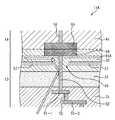
도 1은 본 기술을 적용한 고체 촬상 소자의 제1의 실시의 형태의 구성례를 도시하는 단면도.
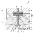
도 2는 고체 촬상 소자의 제2의 구성례를 도시하는 단면도.
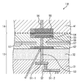
도 3은 고체 촬상 소자의 제3의 구성례를 도시하는 단면도.
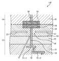
도 4는 고체 촬상 소자의 제4의 구성례를 도시하는 단면도.
도 5는 고체 촬상 소자의 제5의 구성례를 도시하는 단면도.
도 6은 고체 촬상 소자의 제6의 구성례를 도시하는 단면도.
도 7은 고체 촬상 소자의 제7의 구성례를 도시하는 단면도.
도 8은 고체 촬상 소자의 제8의 구성례를 도시하는 단면도.
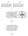
도 9는 고체 촬상 소자의 제조 방법을 설명하는 도면.
도 10은 고체 촬상 소자의 제조 방법을 설명하는 도면.
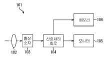
도 11은 촬상 장치의 구성례를 도시하는 블록도.
도 12는 이미지 센서를 사용하는 사용례를 도시하는 도면.1 is a cross-sectional view showing a configuration example of a first embodiment of a solid-state imaging device to which the present technology is applied.
2 is a cross-sectional view showing a second configuration example of a solid-state imaging element.
3 is a cross-sectional view showing a third configuration example of a solid-state imaging element.
4 is a cross-sectional view showing a fourth configuration example of a solid-state imaging element.
5 is a cross-sectional view showing a fifth configuration example of the solid-state imaging element.
6 is a cross-sectional view showing a sixth configuration example of a solid-state imaging element.
7 is a cross-sectional view showing a seventh configuration example of a solid-state imaging element.
8 is a cross-sectional view showing an eighth configuration example of a solid-state imaging device.
9 is an explanatory diagram of a method of manufacturing a solid-state imaging device.
10 is an explanatory diagram of a method of manufacturing a solid-state imaging device.
11 is a block diagram showing a configuration example of an imaging device.
12 is a diagram showing a use case using an image sensor.
이하, 본 기술을 적용한 구체적인 실시의 형태에 관해 도면을 참조하면서 상세히 설명한다.Hereinafter, specific embodiments to which the present technology is applied will be described in detail with reference to the drawings.
<고체 촬상 소자의 제1의 구성례><First configuration example of solid-state imaging element>
도 1은 본 기술을 적용한 고체 촬상 소자의 제1의 실시의 형태의 구성례를 도시하는 도면이다.1 is a diagram showing a configuration example of a first embodiment of a solid-state imaging device to which the present technology is applied.
도 1에는 적층형의 고체 촬상 소자(11)의 단면적인 구성이 도시되어 있고, 도시하는 바와 같이, 고체 촬상 소자(11)는 메모리 기판(12), 로직 기판(13) 및 센서 기판(14)의 3층이 적층되어 구성된다. 또한, 도시되어 있는 파선은 각각의 기판의 접합면을 나타내고 있다.1 shows a cross-sectional configuration of a stacked solid-
메모리 기판(12)은 메모리를 구동하는 복수의 반도체 소자가 형성되는 반도체층(21)에 대해 그들의 반도체 소자를 로직 기판(13) 및 센서 기판(14)과 접속하는데 이용되는 배선이 형성되는 배선층(22)이 적층되어 구성된다.The
로직 기판(13)은 메모리 기판(12)측과의 접속에 이용되는 배선이 형성되는 배선층(31), 로직 회로를 구동하는 반도체 소자가 형성되는 반도체층(32) 및 반도체층(32)측과의 접속에 이용되는 배선이 형성되는 배선층(33)이 적층되어 구성된다.The
센서 기판(14)은 메모리 기판(12) 및 로직 기판(13)과 접속하는데 이용되는 배선이 형성되는 배선층(41), 화소를 구성하는 포토 다이오드나 반도체 소자가 형성되는 반도체층(42) 및 화소마다 광을 집광하는 마이크로 렌즈가 형성되는 온 칩 렌즈층(43)이 적층되어 구성된다.The
또한, 도 1의 하측에는 로직 기판(13) 및 센서 기판(14)의 접합면에서의 구조가 확대하여 도시되어 있다.In addition, the structure at the bonding surface of the
도시하는 바와 같이, 로직 기판(13)의 배선층(31)에는 복수층의 배선(51)(도 1의 예에서는 2층의 배선(51-1 및 51-2)이 배치되어 있고, 그들의 배선(51)은 전극(52)에 의해 접속되어 있다. 그리고, 로직 기판(13)의 반도체층(32)을 관통하도록 형성된 관통 전극(53)에 의해 배선(51-1) 및 콘택트 전극(54)이 접속된다.As shown in the figure, in the
콘택트 전극(54)은 로직 기판(13)의 배선층(33)의 표면, 즉, 로직 기판(13)과 센서 기판(14)과의 접합면에 형성되어 있고, 관통 전극(53)을 센서 기판(14)측에 접속하는데 이용된다. 그리고, 콘택트 전극(54)은 센서 기판(14)측의 접합면에 형성된 콘택트 전극(55)과 접합(예를 들면, Cu-Cu 접합)된다. 또한, 콘택트 전극(55)에는 예를 들면, 센서 기판(14)에 마련된 화소와의 접속을 행하는 전극(56)이 접속되어 있다.The
그리고, 고체 촬상 소자(11)는 로직 기판(13)의 배선층(33)에 차광 메탈막(57)이 형성된 구성으로 되어 있다. 차광 메탈막(57)은 예를 들면, 알루미늄이나, 티탄, 텅스텐, 구리, 탄탈 등의 차광성을 구비한 금속을 성막함에 의해 형성되고, 관통 전극(53)이 형성된 개소가, 개구부(58)에 의해 개구되어 있다. 즉, 관통 전극(53)은 차광 메탈막(57)에 형성된 개구부(58)를 통과하여 배선(51-1) 및 콘택트 전극(54)을 접속한다.In addition, the solid-
또한, 차광 메탈막(57)은 고체 촬상 소자(11)를 평면적으로 보아, 관통 전극(53)이 형성된 부분을 제외한 전면을 덮도록 성막된다. 또한, 차광 메탈막(57)에 형성된 개구부(58)는 고체 촬상 소자(11)를 평면적으로 보아, 콘택트 전극(54)보다도 개구경이 소경이 되도록 형성된다. 즉, 콘택트 전극(54)은 고체 촬상 소자(11)를 평면적으로 보아, 개구부(58)보다도 큰 형상이 되도록 형성된다.In addition, the light-
이와 같이 구성되는 고체 촬상 소자(11)는 차광 메탈막(57)을 마련함에 의해 로직 기판(13)부터 센서 기판(14)으로의 광의 입사를 방지할 수가 있어서, 종래보다도 차광성을 높일 수 있다. 예를 들면, 고체 촬상 소자(11)는 메모리 기판(12)이나 로직 기판(13) 등의 반도체 소자가 구동할 때에 발생하는 핫 캐리어에 기인하는 광을 차광 메탈막(57)에 의해 차광하여 그들의 광이 센서 기판(14)의 화소에 악영향을 미치는 것을 회피할 수 있다.The solid-
특히, 고체 촬상 소자(11)는 차광 메탈막(57)의 개구부(58)보다도 큰 형상의 콘택트 전극(54)을 마련함에 의해 예를 들면, 관통 전극(53)과 차광 메탈막(57)과의 간극을 통과하는 광이 발생하였다고 하여도 그 광을 콘택트 전극(54)에 의해 차단할 수 있다. 이에 의해 로직 기판(13)부터 센서 기판(14)에, 직접적으로, 광이 입사하는 것을 방지할 수 있다.In particular, the solid-
즉, 이와 같은 콘택트 전극(54)에 의해 고체 촬상 소자(11)는 차광 메탈막(57)만을 마련하는 구성보다도 차광성을 높일 수 있다. 또한, 예를 들면, 차광성을 구비하기 위해 전면에 메탈층을 배치하는 구조에서는 관통 전극을 사용할 수가 없음에 대해 고체 촬상 소자(11)는 관통 전극(53)을 사용할 수 있다.That is, the light-shielding property of the solid-
<고체 촬상 소자의 제2 내지 제8의 구성례><Structural examples 2 to 8 of the solid-state imaging element>
도 2 내지 도 8을 참조하여 고체 촬상 소자(11)의 제2 내지 제8의 구성례에 관해 설명한다. 또한, 이하에서 설명하는 고체 촬상 소자(11A 내지 11G)에서, 도 1의 고체 촬상 소자(11)와 공통되는 구성에 관해서는 동일한 부호를 붙이고, 그 상세한 설명은 생략한다.A second to eighth configuration example of the solid-
즉, 고체 촬상 소자(11A 내지 11G)는 도 1의 고체 촬상 소자(11)와 마찬가지로, 메모리 기판(12), 로직 기판(13) 및 센서 기판(14)이 적층된 적층형이고, 로직 기판(13)의 반도체층(32)을 관통하도록 관통 전극(53)이 형성되어 있다. 또한, 고체 촬상 소자(11A 내지 11G)에서도 로직 기판(13)의 센서 기판(14)측에 마련된 배선층(33)에, 관통 전극(53)을 통과시키기 위한 개구부(58)가 형성된 차광 메탈막(57)이 배치되어 있다.That is, the solid-
도 2에는 제2의 구성례인 고체 촬상 소자(11A)의 로직 기판(13) 및 센서 기판(14)의 접합면에서의 단면적인 구성이 도시되어 있다.Fig. 2 shows a cross-sectional configuration in the bonding surface of the
도 2에 도시하는 바와 같이, 고체 촬상 소자(11A)는 차광 메탈막(57)과 콘택트 전극(54)의 사이에, 배선층(33)과는 굴절률이 다른 절연막(61A)이 성막된 구성으로 되어 있다. 예를 들면, 절연막(61A)에는 배선층(33)의 층간 절연막을 구성하는 이산화규소(SiO2)의 굴절률(n1)보다도 절연막(61A)의 굴절률(n2)이 낮게(n2<n1) 되도록 저굴절률의 재질이 선택된다. 또한, 도 2에 도시하는 예에서는 절연막(61A)은 콘택트 전극(54)에 접하는 위치에 배치되어 있지만, 차광 메탈막(57)보다도 콘택트 전극(54)측의 어느 한쪽의 위치에 배치되어 있으면 좋다.As shown in Fig. 2, the solid-
이와 같이 구성되는 고체 촬상 소자(11A)는 로직 기판(13)측으로부터 관통 전극(53) 및 차광 메탈막(57)의 간극을 통과한 광을, 배선층(33)과 절연막(61A)의 계면에서 전반사시킬 수 있다. 즉, 고체 촬상 소자(11A)는 도 2에서 속이 하얀 화살표로 도시하는 바와 같이, 관통 전극(53) 및 차광 메탈막(57)의 간극을 통과한 광을, 고체 촬상 소자(11A)의 측면의 방향을 향하여 전반사시키도록 절연막(61A)이 형성된다. 이에 의해 고체 촬상 소자(11A)에서는 관통 전극(53) 및 차광 메탈막(57)의 간극을 통과한 광이, 센서 기판(14)에 입사하는 것을 회피할 수 있다.The solid-
따라서 고체 촬상 소자(11A)는 배선층(33)과는 굴절률이 다른 절연막(61A)을 마련함으로써, 로직 기판(13)부터 센서 기판(14)으로의 광의 입사를 확실하게 방지할 수가 있어서, 도 1의 고체 촬상 소자(11)보다도 차광성을 높일 수 있다.Therefore, the solid-
다음에, 도 3에는 제3의 구성례인 고체 촬상 소자(11B)의 로직 기판(13) 및 센서 기판(14)의 접합면에서의 단면적인 구성이 도시되어 있다.Next, Fig. 3 shows a cross-sectional configuration at the bonding surface of the
도 3에 도시하는 바와 같이, 고체 촬상 소자(11B)는 관통 전극(53)의 측면을 덮도록 절연막(61B)이 성막된 구성으로 되어 있다. 절연막(61B)은 도 2의 절연막(61A)과 마찬가지로, 저굴절률의 재질이 선택된다.As shown in Fig. 3, the solid-
이와 같이 구성되는 고체 촬상 소자(11B)는 경사 방향부터 관통 전극(53)을 향하여 오는 광을, 배선층(33)과 절연막(61B)의 계면에서 전반사시킬 수 있다. 즉, 고체 촬상 소자(11B)는 도 3에서 속이 하얀 화살표로 도시하는 바와 같이, 경사 방향부터 관통 전극(53)을 향하여 오는 광을, 관통 전극(53)의 긴변 방향에 따르도록 콘택트 전극(54)을 향하여 전반사시키도록 절연막(61B)이 형성된다. 그 광은 콘택트 전극(54)에서 반사하여 로직 기판(13)측으로 되돌아오게 되어, 센서 기판(14)에 입사하는 것을 회피할 수 있다.The solid-
따라서 고체 촬상 소자(11B)는 배선층(33)과는 굴절률이 다른 절연막(61B)을 마련함으로써, 로직 기판(13)부터 센서 기판(14)으로의 광의 입사를 확실하게 방지할 수가 있어서, 도 1의 고체 촬상 소자(11)보다도 차광성을 높일 수 있다.Therefore, the solid-
다음에, 도 4에는 제4의 구성례인 고체 촬상 소자(11C)의 로직 기판(13) 및 센서 기판(14)의 접합면에서의 단면적인 구성이 도시되어 있다.Next, Fig. 4 shows a cross-sectional configuration at the bonding surfaces of the
도 4에 도시하는 바와 같이, 고체 촬상 소자(11C)는 로직 기판(13)측의 접합면이 되는 배선층(33)과는 굴절률이 다른 절연막(61C)이, 센서 기판(14)측의 접합면에 사용된 구성으로 되어 있다. 절연막(61C)은 도 2의 절연막(61A)과 마찬가지로, 저굴절률의 재질이 선택된다. 즉, 절연막(61C)은 로직 기판(13) 및 센서 기판(14)의 접합면에서의 센서 기판(14)측에 마련된다.As shown in Fig. 4, the solid-
이와 같이 구성되는 고체 촬상 소자(11C)는 로직 기판(13)측으로부터 관통 전극(53) 및 차광 메탈막(57)의 간극을 통과한 광을, 배선층(33)과 절연막(61C)의 계면에서, 즉, 로직 기판(13) 및 센서 기판(14)의 접합면에서 전반사시킬 수 있다. 즉, 고체 촬상 소자(11C)는 도 4에서 속이 하얀 화살표로 도시하는 바와 같이, 관통 전극(53) 및 차광 메탈막(57)의 간극을 통과한 광을, 고체 촬상 소자(11C)의 측면의 방향을 향하여 전반사시키도록 절연막(61C)이 형성된다. 이에 의해 고체 촬상 소자(11C)에서는 관통 전극(53) 및 차광 메탈막(57)의 간극을 통과한 광이, 센서 기판(14)에 입사하는 것을 회피할 수 있다.The solid-
따라서 고체 촬상 소자(11C)는 배선층(33)과는 굴절률이 다른 절연막(61C)을 마련함으로써, 로직 기판(13)부터 센서 기판(14)으로의 광의 입사를 확실하게 방지할 수가 있어서, 도 1의 고체 촬상 소자(11)보다도 차광성을 높일 수 있다.Therefore, the solid-
다음에, 도 5에는 제5의 구성례인 고체 촬상 소자(11D)의 로직 기판(13) 및 센서 기판(14)의 접합면에서의 단면적인 구성이 도시되어 있다.Next, FIG. 5 shows a cross-sectional configuration in the bonding surface of the
도 5에 도시하는 바와 같이, 고체 촬상 소자(11D)는 차광 메탈막(57)보다도 센서 기판(14)측에서, 배선층(33)과는 굴절률이 다른 절연막(61D-1)이 이용되고, 관통 전극(53) 및 차광 메탈막(57)의 간극에, 배선층(33)과 절연막(61D-1)의 계면이 마련된 구성으로 되어 있다. 또한, 센서 기판(14)측의 접합면에도 절연막(61D-1)과 같은 굴절률의 절연막(61D-2)이 이용되고 있다. 절연막(61D-1 및 61D-2)은 도 2의 절연막(61A)과 마찬가지로, 저굴절률의 재질이 선택된다. 즉, 절연막(61D)은 차광 메탈막(57)에 적층하도록 차광 메탈막(57)에 대해 센서 기판(14)측에 마련된다.As shown in Fig. 5, the solid-
이와 같이 구성되는 고체 촬상 소자(11D)는 로직 기판(13)측으로부터 관통 전극(53) 및 차광 메탈막(57)의 간극을 향하는 광을, 배선층(33)과 절연막(61D)의 계면에서 전반사시킬 수 있다. 즉, 고체 촬상 소자(11D)는 도 5에서 속이 하얀 화살표로 도시하는 바와 같이, 관통 전극(53) 및 차광 메탈막(57)의 간극을 향하는 광을, 고체 촬상 소자(11D)의 측면의 방향을 향하여 전반사시키도록 절연막(61D)이 형성된다. 이에 의해 고체 촬상 소자(11D)에서는 관통 전극(53) 및 차광 메탈막(57)의 간극을 향하는 광이, 센서 기판(14)에 입사하는 것을 회피할 수 있다.The solid-
따라서 고체 촬상 소자(11D)는 배선층(33)과는 굴절률이 다른 절연막(61D)을 마련함으로써, 로직 기판(13)부터 센서 기판(14)으로의 광의 입사를 확실하게 방지할 수가 있어서, 도 1의 고체 촬상 소자(11)보다도 차광성을 높일 수 있다.Therefore, the solid-
다음에, 도 6에는 제6의 구성례인 고체 촬상 소자(11E)의 로직 기판(13) 및 센서 기판(14)의 접합면에서의 단면적인 구성이 도시되어 있다.Next, Fig. 6 shows a cross-sectional configuration at the bonding surfaces of the
도 6에 도시하는 바와 같이, 고체 촬상 소자(11E)는 로직 기판(13)의 반도체층(32)의, 센서 기판(14)측을 향하는 표면에서 관통 전극(53)이 형성되는 개소에, 차광 메탈막(57)에 형성되는 개구부(58)보다도 큰 형상의 차광 전극(62)이 마련된 구성으로 되어 있다. 예를 들면, 차광 전극(62)은 고체 촬상 소자(11)를 평면적으로 보아, 콘택트 전극(54)과 같은 정도의 크기로 형성된다. 또한, 고체 촬상 소자(11E)의 관통 전극(53)은 차광 전극(62)을 통하여 배선(51-1)과 콘택트 전극(54)을 접속하도록 구성된다.As shown in Fig. 6, the solid-
이와 같이 구성되는 고체 촬상 소자(11E)는 로직 기판(13)측으로부터 관통 전극(53) 및 차광 메탈막(57)의 간극을 향하는 광을, 차광 전극(62)에 의해 차광할 수 있다. 즉, 고체 촬상 소자(11E)는 도 6에서 속이 하얀 화살표로 도시하는 바와 같이, 관통 전극(53) 및 차광 메탈막(57)의 간극을 향하는 광을 차광하도록 차광 전극(62)이 형성된다. 이에 의해 고체 촬상 소자(11E)에서는 관통 전극(53) 및 차광 메탈막(57)의 간극을 향하는 광이, 센서 기판(14)에 입사하는 것을 회피할 수 있다.The solid-
따라서 고체 촬상 소자(11E)는 콘택트 전극(54) 및 차광 전극(62)에 의해 개구부(58)를 끼워 넣는 이중 차광을 구성함으로써, 로직 기판(13)부터 센서 기판(14)으로의 광의 입사를 확실하게 방지할 수가 있어서, 도 1의 고체 촬상 소자(11)보다도 차광성을 높일 수 있다.Therefore, the solid-
다음에, 도 7에는 제7의 구성례인 고체 촬상 소자(11F)의 로직 기판(13) 및 센서 기판(14)의 접합면에서의 단면적인 구성이 도시되어 있다.Next, FIG. 7 shows a cross-sectional configuration in the bonding surface of the
도 7에 도시하는 바와 같이, 고체 촬상 소자(11F)는 로직 기판(13)의 반도체층(32)의, 센서 기판(14)측을 향하는 표면에, 미세한 요철 형상이 주기적으로 구성된 패턴으로 이루어지는 모스아이 구조(63)가 형성된 구성으로 되어 있다. 예를 들면, 모스아이 구조(63)는 광의 반사를 방지하거나, 광을 확산시킬 수 있다.As shown in FIG. 7, the solid-
이와 같이 구성되는 고체 촬상 소자(11F)는 로직 기판(13)측무터 관통 전극(53) 및 차광 메탈막(57)의 간극을 향하는 광이 빠지는 것을, 모스아이 구조(63)에 의해 방지할 수 있다. 즉, 고체 촬상 소자(11F)는 도 7에서 속이 하얀 화살표로 도시하는 바와 같이, 관통 전극(53) 및 차광 메탈막(57)의 간극을 향하는 광이 빠지는 것을 방지하도록 모스아이 구조(63)가 형성된다. 이에 의해 고체 촬상 소자(11F)에서는 관통 전극(53) 및 차광 메탈막(57)의 간극을 향하는 광이, 센서 기판(14)에 입사하는 것을 회피할 수 있다.The solid-
따라서 고체 촬상 소자(11F)는 모스아이 구조(63)를 마련함으로써, 로직 기판(13)부터 센서 기판(14)으로의 광의 입사를 확실하게 방지할 수가 있어서, 도 1의 고체 촬상 소자(11)보다도 차광성을 높일 수 있다.Therefore, the solid-
다음에, 도 8에는 제8의 구성례인 고체 촬상 소자(11G)의 로직 기판(13) 및 센서 기판(14)의 접합면에서의 단면적인 구성이 도시되어 있다.Next, Fig. 8 shows a cross-sectional configuration in the bonding surface of the
도 8에 도시하는 바와 같이, 고체 촬상 소자(11G)는 로직 기판(13)의 반도체층(32)을 관통하는 관통 전극(53G)이, 센서 기판(14)을 향함에 따라 직경이 넓어지는 테이퍼 형상으로 형성된 구성으로 되어 있다.As shown in FIG. 8, the solid-
이와 같이 구성되는 고체 촬상 소자(11G)는 경사 방향부터 관통 전극(53G)을 향하여 오는 광을, 관통 전극(53) 및 차광 메탈막(57)의 간극을 향하는 일이 없는 방향으로 반사시킬 수 있다. 즉, 고체 촬상 소자(11G)는 도 8에서 속이 하얀 화살표로 도시하는 바와 같이, 경사 방향부터 관통 전극(53G)을 향하여 오는 광을, 차광 메탈막(57)의 표면을 향하여 반사시키도록 관통 전극(53G)의 테이퍼 형상이 형성된다. 그 광은 차광 메탈막(57)에서 반사하여 로직 기판(13)의 측면의 방향을 향하게 되어, 센서 기판(14)에 입사하는 것을 회피할 수 있다.The solid-
따라서 고체 촬상 소자(11G)는 테이퍼 형상의 관통 전극(53G)을 마련함으로써, 로직 기판(13)부터 센서 기판(14)으로의 광의 입사를 확실하게 방지할 수가 있어서, 도 1의 고체 촬상 소자(11)보다도 차광성을 높일 수 있다.Therefore, the solid-
예를 들면, 메모리 기판(12) 및 로직 기판(13)부터의 발광은 디바이스 동작 중의 핫 캐리어에 의한 것으로 판명되어 있고, 센서 기판(14)의 하층측으로 부터의 광은 메모리 기판(12) 및 로직 기판(13)에 마련되어 있는 트랜지스터 부근에서 발생한다. 따라서, 이 광원의 방향은 테이퍼 형상의 관통 전극(53G)에서 보아 트랜지스터측의 방향이고, 테이퍼 형상의 관통 전극(53G)의 주변으로의 입사각도는 테이퍼 형상의 관통 전극(53G)에 대한 트랜지스터의 위치 관계에 의존한다.For example, light emission from the
이 때문에, 테이퍼 형상의 관통 전극(53G)의 테이퍼 각도는 입사각에 대한 반사각의 방향으로 차광 메탈막(57)이 존재하도록 설정된다. 즉, 테이퍼 형상의 관통 전극(53G)의 중심축을 수직 방향의 기준으로 하였을 때, 테이퍼 형상의 관통 전극(53G)의 중심축에 대해 트랜지스터로부터 테이퍼 형상의 관통 전극(53G)을 향하는 방향(입사 방향)이 이루는 각도(θ) 및 테이퍼 형상의 관통 전극(53G)의 측면의 각도(φ)에 의거하여 트랜지스터로부터의 광은 테이퍼 형상의 관통 전극(53G)의 측면에서 반사 각도(θ+2φ)로 반사된다.For this reason, the taper angle of the tapered through
따라서 트랜지스터로부터 차광 메탈막(57)까지의 높이에 의존하여 테이퍼 형상의 관통 전극(53G)의 중심부터 각도(2φ) 이내가 되도록 개구부(58)가 형성된 차광 메탈막(57)을 마련함으로써, 트랜지스터로부터의 광을 차광할 수 있다.Therefore, by providing the light-shielding
이상과 같이, 고체 촬상 소자(11) 및 고체 촬상 소자(11A 내지 11D)는 메모리 기판(12), 로직 기판(13) 및 센서 기판(14)이 적층된 적층형이고, 관통 전극(53)에 의해 전기적인 접속을 행하는 구조라도 보다 차광성을 높일 수 있다. 이에 의해 예를 들면, 메모리 기판(12)이나 로직 기판(13) 등의 반도체 소자에서 발생하는 핫 캐리어에 기인하는 광을 차광하여 그와 같은 광이 센서 기판(14)의 화소에 악영향을 미치는 것이 회피된다.As described above, the solid-
또한, 고체 촬상 소자(11)는 차광 메탈막(57)에 대신하여 광을 흡수하는 성질을 구비한 광흡수막을 성막하고, 그 광흡수막에 의해 차광을 행하는 구성으로 하여도 좋다. 또한, 고체 촬상 소자(11)는 메모리 기판(12), 로직 기판(13) 및 센서 기판(14)의 3층 이상의 적층 구조라도 좋다.In addition, the solid-
<고체 촬상 소자의 제조 방법><Method for manufacturing solid-state imaging element>
도 9 및 도 10을 참조하여 도 1의 고체 촬상 소자(11)의 제조 방법에 관해 설명한다.A method of manufacturing the solid-
우선, 제1의 공정에서, 도 9의 상단에 도시하는 바와 같이, 각각 개별적으로 제작된 메모리 기판(12) 및 로직 기판(13)을 하이브리드 접합한다. 예를 들면, 서로의 배선층(22) 및 배선층(31)의 절연막끼리를 접합함과 함께, 도 9에서 확대하여 도시하는 바와 같이, 배선층(22)의 표면에 형성된 콘택트 전극(71)과, 배선층(31)의 표면에 형성된 콘택트 전극(72)을 접합(예를 들면, Cu-Cu 접합)한다.First, in the first process, as shown at the top of FIG. 9, the
또한, 제2의 공정에서, 도 9의 하단에 도시하는 바와 같이, 로직 기판(13)의 반도체층(32)을, 예를 들면, CMP(Chemical Mechanical Polishing) 등을 행하여 박막화한다.In the second step, as shown at the bottom of FIG. 9, the
다음에, 제3의 공정에서, 도 10의 1단째에 도시하는 바와 같이, 반도체층(32)에 대해 배선층(33)이 되는 절연막을 규정의 막두께 이하로 성막하여 그 절연막의 표면의 전면에 대해 차광 메탈막(57)을 성막한다. 그 후, 차광 메탈막(57)에 대해 규정의 막두께가 될 때까지 절연막을 성막함에 의해 차광 메탈막(57)이 끼였던 배선층(33)을 형성한다.Next, in the third step, as shown in the first row of Fig. 10, an insulating film serving as the
또한, 제4의 공정에서, 도 10의 2단째에 도시하는 바와 같이, 반도체층(32)에 접속하도록 관통 전극(53)을 형성함과 함께, 관통 전극(53)에 접속하도록 배선층(33)의 표면에 콘택트 전극(54)을 형성한다. 여기서, 관통 전극(53)을 형성할 때에, 콘택트 전극(54)보다도 개구경이 소경이 되도록 차광 메탈막(57)에 개구부(58)를 가공하고, 개구부(58)를 통과하도록 관통 전극(53)을 형성한다.In the fourth step, as shown in the second stage of Fig. 10, the through
그리고, 제5의 공정에서, 도 10의 3단째에 도시하는 바와 같이, 로직 기판(13)에 대해 센서 기판(14)을 접합한다. 예를 들면, 도 1에 도시한 바와 같이, 로직 기판(13)의 콘택트 전극(54)과, 센서 기판(14)의 콘택트 전극(55)을 접합(예를 들면, Cu-Cu 접합)한다.Then, in the fifth step, as shown in the third stage of Fig. 10, the
이상과 같은 공정을 행하는 제조 장치에 의해 로직 기판(13)부터 센서 기판(14)으로의 광의 입사를 방지하는 차광 메탈막(57)을 구비하여 차광성을 높일 수 있는 고체 촬상 소자(11)를 제조할 수 있다. 또한, 상술한 고체 촬상 소자(11A 내지 11G)도 고체 촬상 소자(11)와 같은 공정으로 제조할 수 있다.A solid-
<전자 기기의 구성례><Configuration examples of electronic devices>
상술한 바와 같은 적층형의 고체 촬상 소자(11)는 예를 들면, 디지털 스틸 카메라나 디지털 비디오 카메라 등의 촬상 시스템, 촬상 기능을 구비한 휴대 전화기, 또는 촬상 기능을 구비한 다른 기기라는 각종의 전자 기기에 적용할 수 있다.The stacked solid-
도 11은 전자 기기에 탑재되는 촬상 장치의 구성례를 도시하는 블록도이다.11 is a block diagram showing a configuration example of an imaging device mounted on an electronic device.
도 11에 도시하는 바와 같이, 촬상 장치(101)는 광학계(102), 촬상 소자(103), 신호 처리 회로(104), 모니터(105) 및 메모리(106)를 구비하여 구성되고, 정지화상 및 동화상을 촬상 가능하다.As shown in FIG. 11, the
광학계(102)는 1장 또는 복수장의 렌즈를 갖고 구성되고, 피사체로부터의 상광(입사광)을 촬상 소자(103)에 유도하여 촬상 소자(103)의 수광면(센서부)에 결상시킨다.The
촬상 소자(103)로서는 상술한 고체 촬상 소자(11)가 적용된다. 촬상 소자(103)에는 광학계(102)를 통하여 수광면에 결상된 상에 응하여 일정 기간, 전자가 축적된다. 그리고, 촬상 소자(103)에 축적된 전자에 응한 신호가 신호 처리 회로(104)에 공급된다.As the
신호 처리 회로(104)는 촬상 소자(103)로부터 출력된 화소 신호에 대해 각종의 신호 처리를 시행한다. 신호 처리 회로(104)가 신호 처리를 시행함에 의해 얻어진 화상(화상 데이터)은 모니터(105)에 공급되어 표시되거나, 메모리(106)에 공급되어 기억(기록)되거나 한다.The
이와 같이 구성되어 있는 촬상 장치(101)에서는 상술한 적층형의 고체 촬상 소자(11)를 적용함으로써, 예를 들면, 핫 캐리어에 기인하는 광에 의한 악영향이 없는 고화질의 화상을 촬상할 수 있다.In the
<이미지 센서의 사용례><Use case of image sensor>
도 12는 상술한 이미지 센서(촬상 소자)를 사용하는 사용례를 도시하는 도면이다.12 is a diagram showing a use case using the above-described image sensor (imaging element).
상술한 이미지 센서는 예를 들면, 이하와 같이, 가시광이나, 적외광, 자외광, X선 등의 광을 센싱하는 다양한 케이스에 사용할 수 있다.The image sensor described above can be used in various cases for sensing light such as visible light, infrared light, ultraviolet light, and X-rays, for example, as follows.
·디지털 카메라나, 카메라 기능 부착의 휴대 기기 등의, 감상용으로 제공되는 화상을 촬영하는 장치·A device that shoots images provided for viewing, such as digital cameras or mobile devices with camera functions
·자동 정지 등의 안전운전이나, 운전자의 상태의 인식 등을 위해 자동차의 전방이나 후방, 주위, 차내 등을 촬영하는 차량탑재용 센서, 주행 차량이나 도로를 감시하는 감시 카메라, 차량 사이 등의 거리측정을 행하는 거리측정 센서 등의, 교통용으로 제공되는 장치·Vehicle-mounted sensors that take pictures of the front or rear, surroundings, and the inside of a vehicle for safe driving such as automatic stop, and recognition of the driver's condition, surveillance cameras that monitor driving vehicles or roads, and distances between vehicles Devices provided for transportation, such as distance measuring sensors for measuring
·유저의 제스처를 촬영하고, 그 제스처에 따른 기기 조작을 행하기 위해 TV나, 냉장고, 에어 컨디셔너 등의 가전에 제공되는 장치Devices provided to household appliances, such as TVs, refrigerators, and air conditioners, to shoot user gestures and perform device manipulations
·내시경이나, 적외광의 수광에 의한 혈관 촬영을 행하는 장치 등의, 의료나 헬스케어용으로 제공되는 장치Devices provided for medical or health care, such as endoscopes and devices that take blood vessels by receiving infrared light
·방범 용도의 감시 카메라나, 인물 인증 용도의 카메라 등의, 시큐리티용으로 제공되는 장치Devices provided for security purposes, such as surveillance cameras for security purposes or cameras for person authentication
·피부를 촬영한 피부측정기나, 두피를 촬영하는 마이크로스코프 등의, 미용용으로 제공되는 장치·A device provided for cosmetic purposes, such as a skin measuring device that photographs the skin or a microscope that photographs the scalp
·스포츠 용도 등 용의 액션 카메라나 웨어러블 카메라 등의, 스포츠용으로 제공되는 장치Devices provided for sports, such as action cameras and wearable cameras for sports use, etc.
·밭이나 작물의 상태를 감시하기 위한 카메라 등의, 농업용으로 제공되는 장치·A device provided for agriculture, such as a camera for monitoring the condition of a field or crop
<구성의 조합례><Composition of the composition>
또한, 본 기술은 이하와 같은 구성도 취할 수 있다.In addition, the present technology can also take the following configurations.
(1) 제1의 기판, 제2의 기판 및 제3의 기판이 적층된 적층 구조의 상기 제2의 기판의 반도체층을 관통하도록 상기 제1의 기판측 및 상기 제3의 기판측을 접속하는 관통 전극과,(1) connecting the first substrate side and the third substrate side so as to penetrate through the semiconductor layer of the second substrate in a stacked structure in which a first substrate, a second substrate and a third substrate are stacked. A through electrode,
상기 제3의 기판측에 마련되는 상기 제2의 기판의 배선층에 배치되고, 상기 관통 전극을 통과하도록 개구하는 개구부가 형성된 차광막과,A light shielding film disposed on the wiring layer of the second substrate provided on the third substrate side, and having an opening opening through the through electrode;
상기 제2의 기판 및 상기 제3의 기판의 접합면에 형성되고, 상기 관통 전극을 상기 제3의 기판측에 접속하는데 이용되는 콘택트 전극을 구비하는 고체 촬상 소자.A solid-state imaging element formed on a bonding surface between the second substrate and the third substrate, and comprising a contact electrode used to connect the through electrode to the third substrate side.
(2) 상기 차광막에 형성되는 상기 개구부는 상기 고체 촬상 소자를 평면적으로 보아, 상기 콘택트 전극보다도 소경으로 형성되는 상기 (1)에 기재된 고체 촬상 소자.(2) The solid-state imaging element according to (1), wherein the opening formed in the light-shielding film is formed to have a smaller diameter than the contact electrode when the solid-state imaging element is viewed planarly.
(3) 상기 차광막보다도 상기 콘택트 전극측에, 상기 제2의 기판의 상기 배선층과는 굴절률이 다른 절연막이 성막되는 상기 (1) 또는 (2)에 기재된 고체 촬상 소자.(3) The solid-state imaging element according to (1) or (2), wherein an insulating film having a refractive index different from that of the wiring layer of the second substrate is formed on the contact electrode side than the light-shielding film.
(4) 상기 관통 전극의 측면을 덮도록 상기 제2의 기판의 상기 배선층과는 굴절률이 다른 절연막이 성막되는 상기 (1)부터 (3)까지의 어느 하나에 기재된 고체 촬상 소자.(4) The solid-state imaging device according to any one of (1) to (3), wherein an insulating film having a refractive index different from that of the wiring layer of the second substrate is formed so as to cover the side surface of the through electrode.
(5) 상기 제2의 기판의 상기 배선층과는 굴절률이 다른 절연막이, 상기 제2의 기판 및 상기 제3의 기판의 접합면에서의 상기 제3의 기판측에 마련되는 상기 (1)부터 (4)까지의 어느 하나에 기재된 고체 촬상 소자.(5) From (1) to (3), an insulating film having a different refractive index from the wiring layer of the second substrate is provided on the third substrate side at the bonding surfaces of the second substrate and the third substrate. The solid-state imaging element described in any one up to 4).
(6) 상기 제2의 기판의 상기 배선층과는 굴절률이 다른 절연막이, 상기 차광막에 적층하도록 상기 차광막의 상기 제3의 기판측에 마련되는 상기 (1)부터 (5)까지의 어느 하나에 기재된 고체 촬상 소자.(6) described in any one of (1) to (5) above, wherein an insulating film having a different refractive index from the wiring layer of the second substrate is provided on the third substrate side of the light shielding film so as to be laminated on the light shielding film. Solid-state imaging device.
(7) 상기 제3의 기판측을 향하는 상기 제2의 기판의 상기 반도체층의 표면에서 상기 관통 전극이 형성되는 개소에 형성되고, 상기 차광막에 형성되는 상기 개구부보다 큰 형상의 차광 전극을 또한 구비하는 상기 (1)부터 (6)까지의 어느 하나에 기재된 고체 촬상 소자.(7) A light-blocking electrode having a shape larger than the opening formed in the light-shielding film is formed at a portion where the through-electrode is formed on the surface of the semiconductor layer of the second substrate facing the third substrate. The solid-state imaging element described in any one of (1) to (6) above.
(8) 상기 제3의 기판측을 향하는 상기 제2의 기판의 상기 반도체층의 표면에, 미세한 요철 형상이 주기적으로 구성된 패턴으로 이루어지는 모스아이 구조가 형성되는 상기 (1)부터 (7)까지의 어느 하나에 기재된 고체 촬상 소자.(8) From (1) to (7) above, a moth-eye structure is formed on the surface of the semiconductor layer of the second substrate facing the third substrate, in a pattern in which fine irregularities are periodically formed. The solid-state imaging element according to any one.
(9) 상기 관통 전극이, 상기 제3의 기판을 향함에 따라 직경이 넓어지는 테이퍼 형상으로 형성되는 상기 (1)부터 (8)까지의 어느 하나에 기재된 고체 촬상 소자.(9) The solid-state imaging device according to any one of (1) to (8), wherein the through electrode is formed in a tapered shape that increases in diameter as it faces the third substrate.
(10) 제1의 기판, 제2의 기판 및 제3의 기판이 적층된 적층 구조의 상기 제2의 기판의 반도체층을 관통하도록 상기 제1의 기판측 및 상기 제3의 기판측을 접속하는 관통 전극과,(10) connecting the first substrate side and the third substrate side so as to penetrate through the semiconductor layer of the second substrate in a stacked structure in which a first substrate, a second substrate and a third substrate are stacked. A through electrode,
상기 제3의 기판측에 마련되는 상기 제2의 기판의 배선층에 배치되고, 상기 관통 전극을 통과하도록 개구하는 개구부가 형성된 차광막과,A light shielding film disposed on the wiring layer of the second substrate provided on the third substrate side, and having an opening opening through the through electrode;
상기 제2의 기판 및 상기 제3의 기판의 접합면에 형성되고, 상기 관통 전극을 상기 제3의 기판측에 접속하는데 이용되는 콘택트 전극을 구비하는 고체 촬상 소자를 제조하는 제조 장치가 상기 제1의 기판과 상기 제2의 기판을 접합하는 것과,A manufacturing apparatus for manufacturing a solid-state imaging device formed on a bonding surface of the second substrate and the third substrate and having a contact electrode used to connect the through electrode to the third substrate side is the first. Bonding the substrate and the second substrate of,
상기 제2의 기판의 배선층이 되는 절연막을 규정의 막두께 이하로 성막하여 그 절연막의 표면의 전면에 대해 상기 차광막을 성막한 후에, 규정의 막두께가 될 때까지 절연막을 성막하여 상기 제2의 기판의 배선층을 형성하는 것과,After forming the insulating film to be the wiring layer of the second substrate to a thickness less than or equal to a prescribed film thickness, and forming the light-shielding film on the entire surface of the insulating film, the film is formed until the film thickness becomes the specified film thickness. Forming a wiring layer of the substrate,
상기 차광막에 상기 개구부를 개구하고, 그 개구부를 통과하도록 상기 관통 전극을 형성한 후에, 상기 관통 전극에 접속하도록 상기 제2의 기판의 배선층의 표면에 상기 콘택트 전극을 형성하는 것과,Opening the opening in the light shielding film and forming the through electrode to pass through the opening, and then forming the contact electrode on the surface of the wiring layer of the second substrate to connect to the through electrode,
상기 제2의 기판과 상기 제3의 기판을 접합하는 것을 포함하는 제조 방법.A manufacturing method comprising bonding the second substrate and the third substrate.
(11) 제1의 기판, 제2의 기판 및 제3의 기판이 적층된 적층 구조의 고체 촬상 소자와,(11) a solid-state imaging device having a stacked structure in which a first substrate, a second substrate, and a third substrate are stacked;
상기 제2의 기판의 반도체층을 관통하도록 상기 제1의 기판측 및 상기 제3의 기판측을 접속하는 관통 전극과,A through electrode connecting the first substrate side and the third substrate side to penetrate the semiconductor layer of the second substrate;
상기 제3의 기판측에 마련되는 상기 제2의 기판의 배선층에 배치되고, 상기 관통 전극을 통과하도록 개구하는 개구부가 형성된 차광막과,A light shielding film disposed on the wiring layer of the second substrate provided on the third substrate side, and having an opening opening through the through electrode;
상기 제2의 기판 및 상기 제3의 기판의 접합면에 형성되고, 상기 관통 전극을 상기 제3의 기판측에 접속하는데 이용되는 콘택트 전극을 갖는 고체 촬상 소자를 구비하는 전자 기기.An electronic device comprising a solid-state imaging element formed on a bonding surface between the second substrate and the third substrate, and having a contact electrode used to connect the through electrode to the third substrate.
또한, 본 실시의 형태는 상술한 실시의 형태로 한정되는 것이 아니고, 본 개시의 요지를 일탈하지 않는 범위에서 여러가지의 변경이 가능하다. 또한, 본 명세서에 기재된 효과는 어디까지나 예시이고 한정되는 것이 아니고, 다른 효과가 있어도 좋다.In addition, the present embodiment is not limited to the above-described embodiment, and various changes can be made without departing from the gist of the present disclosure. In addition, the effects described in the present specification are only examples and are not limited, and other effects may be used.
11 : 고체 촬상 소자 12 : 메모리 기판
13층: 로직 기판 14 : 센서 기판
21 : 반도체층 22 : 배선층
31 : 배선층 32 : 반도체층
33 : 배선층 41 : 배선층
42 : 반도체층 43층: 온 칩 렌즈층
51 : 배선 52 : 전극
53 : 관통 전극 54 및 55 : 콘택트 전극
56 : 전극 57 : 차광 메탈막
58 : 개구부 61 : 절연막
62 : 차광 전극 63층: 모스아이 구조11: solid-state imaging element 12: memory substrate
13th layer: logic board 14: sensor board
21: semiconductor layer 22: wiring layer
31: wiring layer 32: semiconductor layer
33: wiring layer 41: wiring layer
42:
51: wiring 52: electrode
53: through
56: electrode 57: light-shielding metal film
58: opening 61: insulating film
62:
Claims (11)
상기 제3의 기판측에 마련되는 상기 제2의 기판의 배선층에 배치되고, 상기 관통 전극을 통과하도록 개구하는 개구부가 형성된 차광막과,
상기 제2의 기판 및 상기 제3의 기판의 접합면에 형성되고, 상기 관통 전극을 상기 제3의 기판측에 접속하는데 이용되는 콘택트 전극을 구비하는 것을 특징으로 하는 고체 촬상 소자.A through electrode connecting the first substrate side and the third substrate side so as to penetrate through the semiconductor layer of the second substrate in a stacked structure in which a first substrate, a second substrate and a third substrate are stacked; ,
A light shielding film disposed on a wiring layer of the second substrate provided on the third substrate side, and having an opening opening through the through electrode;
And a contact electrode formed on a bonding surface between the second substrate and the third substrate and used to connect the through electrode to the third substrate side.
상기 차광막에 형성되는 상기 개구부는 상기 고체 촬상 소자를 평면적으로 보아, 상기 콘택트 전극보다도 소경으로 형성되는 것을 특징으로 하는 고체 촬상 소자.According to claim 1,
The opening formed in the light-shielding film is a solid-state imaging device characterized in that the solid-state imaging device is formed in a smaller diameter than the contact electrode when viewed in plan view.
상기 차광막보다도 상기 콘택트 전극측에, 상기 제2의 기판의 상기 배선층과는 굴절률이 다른 절연막이 성막되는 것을 특징으로 하는 고체 촬상 소자.According to claim 2,
A solid-state imaging element characterized in that an insulating film having a refractive index different from that of the wiring layer of the second substrate is formed on the contact electrode side than the light-shielding film.
상기 관통 전극의 측면을 덮도록 상기 제2의 기판의 상기 배선층과는 굴절률이 다른 절연막이 성막되는 것을 특징으로 하는 고체 촬상 소자.According to claim 2,
A solid-state imaging device, characterized in that an insulating film having a refractive index different from that of the wiring layer of the second substrate is formed to cover the side surface of the through electrode.
상기 제2의 기판의 상기 배선층과는 굴절률이 다른 절연막이, 상기 제2의 기판 및 상기 제3의 기판의 접합면에서의 상기 제3의 기판측에 마련되는 것을 특징으로 하는 고체 촬상 소자.According to claim 2,
A solid-state imaging device, characterized in that an insulating film having a different refractive index from the wiring layer of the second substrate is provided on the side of the third substrate at the bonding surfaces of the second substrate and the third substrate.
상기 제2의 기판의 상기 배선층과는 굴절률이 다른 절연막이, 상기 차광막에 적층하도록 상기 차광막의 상기 제3의 기판측에 마련되는 것을 특징으로 하는 고체 촬상 소자.According to claim 2,
A solid-state imaging device, characterized in that an insulating film having a different refractive index from the wiring layer of the second substrate is provided on the third substrate side of the light-shielding film so as to be laminated on the light-shielding film.
상기 제3의 기판측을 향하는 상기 제2의 기판의 상기 반도체층의 표면에서 상기 관통 전극이 형성되는 개소에 형성되고, 상기 차광막에 형성되는 상기 개구부보다 큰 형상의 차광 전극을 또한 구비하는 것을 특징으로 하는 고체 촬상 소자.According to claim 2,
It is formed on the surface of the semiconductor layer of the second substrate facing the third substrate side, and is provided at a portion where the through electrode is formed, and further comprising a light blocking electrode having a shape larger than the opening formed in the light blocking film. Solid-state imaging device.
상기 제3의 기판측을 향하는 상기 제2의 기판의 상기 반도체층의 표면에, 미세한 요철 형상이 주기적으로 구성된 패턴으로 이루어지는 모스아이 구조가 형성되는 것을 특징으로 하는 고체 촬상 소자.According to claim 2,
A solid-state imaging device, characterized in that a mos-eye structure is formed on a surface of the semiconductor layer of the second substrate facing the third substrate side in a pattern in which fine irregularities are periodically formed.
상기 관통 전극이, 상기 제3의 기판을 향함에 따라 직경이 넓어지는 테이퍼 형상으로 형성되는 것을 특징으로 하는 고체 촬상 소자.According to claim 2,
A solid-state imaging device, characterized in that the through electrode is formed in a tapered shape that increases in diameter as it faces the third substrate.
상기 제3의 기판측에 마련되는 상기 제2의 기판의 배선층에 배치되고, 상기 관통 전극을 통과하도록 개구하는 개구부가 형성된 차광막과,
상기 제2의 기판 및 상기 제3의 기판의 접합면에 형성되고, 상기 관통 전극을 상기 제3의 기판측에 접속하는데 이용되는 콘택트 전극을 구비하는 고체 촬상 소자를 제조하는 제조 장치가,
상기 제1의 기판과 상기 제2의 기판을 접합하는 것과,
상기 제2의 기판의 배선층이 되는 절연막을 규정의 막두께 이하로 성막하여 그 절연막의 표면의 전면에 대해 상기 차광막을 성막한 후에, 규정의 막두께로 될 때까지 절연막을 성막하여 상기 제2의 기판의 배선층을 형성하는 것과,
상기 차광막에 상기 개구부를 개구하고, 그 개구부를 통과하도록 상기 관통 전극을 형성한 후에, 상기 관통 전극에 접속하도록 상기 제2의 기판의 배선층의 표면에 상기 콘택트 전극을 형성하는 것과,
상기 제2의 기판과 상기 제3의 기판을 접합하는 것을 포함하는 것을 특징으로 하는 제조 방법.A through electrode connecting the first substrate side and the third substrate side so as to penetrate through the semiconductor layer of the second substrate in a stacked structure in which a first substrate, a second substrate and a third substrate are stacked; ,
A light shielding film disposed on a wiring layer of the second substrate provided on the third substrate side, and having an opening opening through the through electrode;
A manufacturing apparatus for manufacturing a solid-state imaging element formed on a bonding surface of the second substrate and the third substrate and having a contact electrode used to connect the through electrode to the third substrate side,
Bonding the first substrate and the second substrate,
After forming the insulating film to be the wiring layer of the second substrate to a thickness less than or equal to a prescribed film thickness, and forming the light shielding film on the entire surface of the insulating film, an insulating film is formed until a prescribed film thickness is obtained. Forming a wiring layer of the substrate,
Opening the opening in the light shielding film and forming the through electrode to pass through the opening, and then forming the contact electrode on the surface of the wiring layer of the second substrate to connect to the through electrode,
And bonding the second substrate to the third substrate.
상기 제2의 기판의 반도체층을 관통하도록 상기 제1의 기판측 및 상기 제3의 기판측을 접속하는 관통 전극과,
상기 제3의 기판측에 마련되는 상기 제2의 기판의 배선층에 배치되고, 상기 관통 전극을 통과하도록 개구하는 개구부가 형성된 차광막과,
상기 제2의 기판 및 상기 제3의 기판의 접합면에 형성되고, 상기 관통 전극을 상기 제3의 기판측에 접속하는데 이용되는 콘택트 전극을 갖는 고체 촬상 소자를 구비하는 것을 특징으로 하는 전자 기기.A solid-state imaging device having a stacked structure in which a first substrate, a second substrate, and a third substrate are stacked;
A through electrode connecting the first substrate side and the third substrate side to penetrate the semiconductor layer of the second substrate;
A light shielding film disposed on a wiring layer of the second substrate provided on the third substrate side, and having an opening opening through the through electrode;
And a solid-state imaging device formed on a bonding surface between the second substrate and the third substrate, and having a contact electrode used to connect the through electrode to the third substrate side.
Applications Claiming Priority (3)
| Application Number | Priority Date | Filing Date | Title |
|---|---|---|---|
| JPJP-P-2017-214326 | 2017-11-07 | ||
| JP2017214326 | 2017-11-07 | ||
| PCT/JP2018/039408 WO2019093122A1 (en) | 2017-11-07 | 2018-10-24 | Solid-state image pickup element, manufacturing method, and electronic apparatus |
Publications (2)
| Publication Number | Publication Date |
|---|---|
| KR20200078480A true KR20200078480A (en) | 2020-07-01 |
| KR102667054B1 KR102667054B1 (en) | 2024-05-20 |
Family
ID=66438410
Family Applications (1)
| Application Number | Title | Priority Date | Filing Date |
|---|---|---|---|
| KR1020207007640A Active KR102667054B1 (en) | 2017-11-07 | 2018-10-24 | Solid-state imaging device, manufacturing method, and electronic device |
Country Status (4)
| Country | Link |
|---|---|
| US (1) | US11594564B2 (en) |
| KR (1) | KR102667054B1 (en) |
| CN (1) | CN111295762B (en) |
| WO (1) | WO2019093122A1 (en) |
Cited By (1)
| Publication number | Priority date | Publication date | Assignee | Title |
|---|---|---|---|---|
| US12402430B2 (en) | 2021-05-18 | 2025-08-26 | Samsung Electronics Co., Ltd. | Image sensor |
Families Citing this family (2)
| Publication number | Priority date | Publication date | Assignee | Title |
|---|---|---|---|---|
| JP2020047616A (en) * | 2018-09-14 | 2020-03-26 | ソニーセミコンダクタソリューションズ株式会社 | Solid-state imaging device and electronic equipment |
| WO2024202677A1 (en) * | 2023-03-31 | 2024-10-03 | ソニーセミコンダクタソリューションズ株式会社 | Light detection device |
Citations (5)
| Publication number | Priority date | Publication date | Assignee | Title |
|---|---|---|---|---|
| KR20120028799A (en) * | 2010-09-15 | 2012-03-23 | 소니 주식회사 | Solid state imaging device and electronic apparatus |
| JP2012164870A (en) | 2011-02-08 | 2012-08-30 | Sony Corp | Solid state image pickup device, manufacturing method of the same and electronic equipment |
| US20150097258A1 (en) * | 2013-10-09 | 2015-04-09 | Sony Corporation | Semiconductor device, manufacturing method thereof, and electronic apparatus |
| KR20150113133A (en) * | 2013-01-31 | 2015-10-07 | 애플 인크. | Vertically stacked image sensor |
| JP2017073436A (en) * | 2015-10-06 | 2017-04-13 | ソニーセミコンダクタソリューションズ株式会社 | Solid-state imaging device and electronic device |
Family Cites Families (9)
| Publication number | Priority date | Publication date | Assignee | Title |
|---|---|---|---|---|
| JP3434740B2 (en) * | 1999-06-30 | 2003-08-11 | Necエレクトロニクス株式会社 | Solid-state imaging device |
| US8212297B1 (en) * | 2011-01-21 | 2012-07-03 | Hong Kong Applied Science and Technology Research Institute Company Limited | High optical efficiency CMOS image sensor |
| TWI577001B (en) * | 2011-10-04 | 2017-04-01 | 新力股份有限公司 | Solid-state imaging device, method of manufacturing solid-state imaging device, and electronic device |
| JP2013187360A (en) * | 2012-03-08 | 2013-09-19 | Sony Corp | Solid-state image pickup device and electronic apparatus |
| US8946784B2 (en) * | 2013-02-18 | 2015-02-03 | Taiwan Semiconductor Manufacturing Company, Ltd. | Method and apparatus for image sensor packaging |
| US9536777B2 (en) * | 2013-03-13 | 2017-01-03 | Taiwan Semiconductor Manufacutring Company, Ltd. | Interconnect apparatus and method |
| JP6303803B2 (en) * | 2013-07-03 | 2018-04-04 | ソニー株式会社 | Solid-state imaging device and manufacturing method thereof |
| KR102544782B1 (en) * | 2016-08-04 | 2023-06-20 | 삼성전자주식회사 | semiconductor package and method for manufacturing the same |
| US9947705B1 (en) * | 2016-09-26 | 2018-04-17 | Semiconductor Components Industries, Llc | Image sensors with infrared-blocking layers |
-
2018
- 2018-10-24 WO PCT/JP2018/039408 patent/WO2019093122A1/en not_active Ceased
- 2018-10-24 CN CN201880070348.4A patent/CN111295762B/en active Active
- 2018-10-24 US US16/759,901 patent/US11594564B2/en active Active
- 2018-10-24 KR KR1020207007640A patent/KR102667054B1/en active Active
Patent Citations (5)
| Publication number | Priority date | Publication date | Assignee | Title |
|---|---|---|---|---|
| KR20120028799A (en) * | 2010-09-15 | 2012-03-23 | 소니 주식회사 | Solid state imaging device and electronic apparatus |
| JP2012164870A (en) | 2011-02-08 | 2012-08-30 | Sony Corp | Solid state image pickup device, manufacturing method of the same and electronic equipment |
| KR20150113133A (en) * | 2013-01-31 | 2015-10-07 | 애플 인크. | Vertically stacked image sensor |
| US20150097258A1 (en) * | 2013-10-09 | 2015-04-09 | Sony Corporation | Semiconductor device, manufacturing method thereof, and electronic apparatus |
| JP2017073436A (en) * | 2015-10-06 | 2017-04-13 | ソニーセミコンダクタソリューションズ株式会社 | Solid-state imaging device and electronic device |
Cited By (1)
| Publication number | Priority date | Publication date | Assignee | Title |
|---|---|---|---|---|
| US12402430B2 (en) | 2021-05-18 | 2025-08-26 | Samsung Electronics Co., Ltd. | Image sensor |
Also Published As
| Publication number | Publication date |
|---|---|
| WO2019093122A1 (en) | 2019-05-16 |
| KR102667054B1 (en) | 2024-05-20 |
| CN111295762B (en) | 2024-10-22 |
| US11594564B2 (en) | 2023-02-28 |
| US20210183931A1 (en) | 2021-06-17 |
| CN111295762A (en) | 2020-06-16 |
Similar Documents
| Publication | Publication Date | Title |
|---|---|---|
| US11437423B2 (en) | Image sensor, manufacturing method, and electronic device | |
| US10425624B2 (en) | Solid-state image capturing device and electronic device | |
| KR102708230B1 (en) | Semiconductor device and manufacturing method, and electronic appliance | |
| US20210302634A1 (en) | Semiconductor chip and electronic apparatus | |
| CN104681572A (en) | Solid-state imaging device and electronic apparatus | |
| WO2016203990A1 (en) | Image capturing element, electronic device | |
| JP2014157885A (en) | Semiconductor substrate, image pickup element and image pickup apparatus | |
| US12218167B2 (en) | Solid-state imaging device and electronic device | |
| CN109478555B (en) | Solid-state imaging element, manufacturing method, and electronic device | |
| US20250072136A1 (en) | Semiconductor Device, Solid-State Image Pickup Element, Imaging Device, and Electronic Apparatus | |
| KR102389418B1 (en) | Solid-state imaging devices and electronic devices | |
| CN108701696A (en) | Glass intermediary layer module, imaging device and electronic equipment | |
| US20170221956A1 (en) | Solid-state imaging device and imaging apparatus | |
| JP2018046040A (en) | SOLID-STATE IMAGING DEVICE, MANUFACTURING METHOD THEREOF, AND ELECTRONIC DEVICE | |
| KR102667054B1 (en) | Solid-state imaging device, manufacturing method, and electronic device | |
| US11818473B2 (en) | Ultrathin camera device using microlens array, and multi-functional imaging method using the same | |
| WO2016163242A1 (en) | Solid-state image capture element and electronic device | |
| WO2017119317A1 (en) | Solid state imaging element, production method, and electronic apparatus | |
| US10823975B2 (en) | Methods and apparatus for a polarizing image sensor | |
| KR20250172936A (en) | Solid-state imaging device and manufacturing method, and electronic device | |
| WO2017073335A1 (en) | Solid-state imaging element, production method, and electronic apparatus | |
| TW202450088A (en) | Solid-state imaging devices and electronic devices | |
| JPWO2017068713A1 (en) | Solid-state imaging device and imaging device | |
| WO2016194577A1 (en) | Imaging element, imaging method, program, and electronic device | |
| WO2016098594A1 (en) | Semiconductor device, solid-state imaging element, imaging device, and electronic device |
Legal Events
| Date | Code | Title | Description |
|---|---|---|---|
| PA0105 | International application |
St.27 status event code: A-0-1-A10-A15-nap-PA0105 |
|
| PG1501 | Laying open of application |
St.27 status event code: A-1-1-Q10-Q12-nap-PG1501 |
|
| PA0201 | Request for examination |
St.27 status event code: A-1-2-D10-D11-exm-PA0201 |
|
| P22-X000 | Classification modified |
St.27 status event code: A-2-2-P10-P22-nap-X000 |
|
| P22-X000 | Classification modified |
St.27 status event code: A-2-2-P10-P22-nap-X000 |
|
| E902 | Notification of reason for refusal | ||
| PE0902 | Notice of grounds for rejection |
St.27 status event code: A-1-2-D10-D21-exm-PE0902 |
|
| E13-X000 | Pre-grant limitation requested |
St.27 status event code: A-2-3-E10-E13-lim-X000 |
|
| P11-X000 | Amendment of application requested |
St.27 status event code: A-2-2-P10-P11-nap-X000 |
|
| P13-X000 | Application amended |
St.27 status event code: A-2-2-P10-P13-nap-X000 |
|
| E90F | Notification of reason for final refusal | ||
| PE0902 | Notice of grounds for rejection |
St.27 status event code: A-1-2-D10-D21-exm-PE0902 |
|
| P11-X000 | Amendment of application requested |
St.27 status event code: A-2-2-P10-P11-nap-X000 |
|
| P13-X000 | Application amended |
St.27 status event code: A-2-2-P10-P13-nap-X000 |
|
| E701 | Decision to grant or registration of patent right | ||
| PE0701 | Decision of registration |
St.27 status event code: A-1-2-D10-D22-exm-PE0701 |
|
| GRNT | Written decision to grant | ||
| PR0701 | Registration of establishment |
St.27 status event code: A-2-4-F10-F11-exm-PR0701 |
|
| PR1002 | Payment of registration fee |
St.27 status event code: A-2-2-U10-U12-oth-PR1002 Fee payment year number: 1 |
|
| PG1601 | Publication of registration |
St.27 status event code: A-4-4-Q10-Q13-nap-PG1601 |
|
| P22-X000 | Classification modified |
St.27 status event code: A-4-4-P10-P22-nap-X000 |
|
| P22-X000 | Classification modified |
St.27 status event code: A-4-4-P10-P22-nap-X000 |