KR20200083330A - Plasma processing apparatus and control method - Google Patents
Plasma processing apparatus and control method Download PDFInfo
- Publication number
- KR20200083330A KR20200083330A KR1020190176574A KR20190176574A KR20200083330A KR 20200083330 A KR20200083330 A KR 20200083330A KR 1020190176574 A KR1020190176574 A KR 1020190176574A KR 20190176574 A KR20190176574 A KR 20190176574A KR 20200083330 A KR20200083330 A KR 20200083330A
- Authority
- KR
- South Korea
- Prior art keywords
- voltage
- state
- electrode
- plasma
- power supply
- Prior art date
- Legal status (The legal status is an assumption and is not a legal conclusion. Google has not performed a legal analysis and makes no representation as to the accuracy of the status listed.)
- Granted
Links
Images


Classifications
-
- H—ELECTRICITY
- H01—ELECTRIC ELEMENTS
- H01J—ELECTRIC DISCHARGE TUBES OR DISCHARGE LAMPS
- H01J37/00—Discharge tubes with provision for introducing objects or material to be exposed to the discharge, e.g. for the purpose of examination or processing thereof
- H01J37/32—Gas-filled discharge tubes
- H01J37/32009—Arrangements for generation of plasma specially adapted for examination or treatment of objects, e.g. plasma sources
- H01J37/32082—Radio frequency generated discharge
- H01J37/32137—Radio frequency generated discharge controlling of the discharge by modulation of energy
- H01J37/32146—Amplitude modulation, includes pulsing
-
- H—ELECTRICITY
- H01—ELECTRIC ELEMENTS
- H01J—ELECTRIC DISCHARGE TUBES OR DISCHARGE LAMPS
- H01J37/00—Discharge tubes with provision for introducing objects or material to be exposed to the discharge, e.g. for the purpose of examination or processing thereof
- H01J37/32—Gas-filled discharge tubes
- H01J37/32009—Arrangements for generation of plasma specially adapted for examination or treatment of objects, e.g. plasma sources
- H01J37/32082—Radio frequency generated discharge
-
- H—ELECTRICITY
- H01—ELECTRIC ELEMENTS
- H01J—ELECTRIC DISCHARGE TUBES OR DISCHARGE LAMPS
- H01J37/00—Discharge tubes with provision for introducing objects or material to be exposed to the discharge, e.g. for the purpose of examination or processing thereof
- H01J37/32—Gas-filled discharge tubes
- H01J37/32009—Arrangements for generation of plasma specially adapted for examination or treatment of objects, e.g. plasma sources
- H01J37/32082—Radio frequency generated discharge
- H01J37/32174—Circuits specially adapted for controlling the RF discharge
- H01J37/32183—Matching circuits
-
- H—ELECTRICITY
- H01—ELECTRIC ELEMENTS
- H01J—ELECTRIC DISCHARGE TUBES OR DISCHARGE LAMPS
- H01J37/00—Discharge tubes with provision for introducing objects or material to be exposed to the discharge, e.g. for the purpose of examination or processing thereof
- H01J37/32—Gas-filled discharge tubes
- H01J37/32431—Constructional details of the reactor
- H01J37/32532—Electrodes
-
- H—ELECTRICITY
- H01—ELECTRIC ELEMENTS
- H01J—ELECTRIC DISCHARGE TUBES OR DISCHARGE LAMPS
- H01J37/00—Discharge tubes with provision for introducing objects or material to be exposed to the discharge, e.g. for the purpose of examination or processing thereof
- H01J37/32—Gas-filled discharge tubes
- H01J37/32431—Constructional details of the reactor
- H01J37/32623—Mechanical discharge control means
-
- H—ELECTRICITY
- H01—ELECTRIC ELEMENTS
- H01J—ELECTRIC DISCHARGE TUBES OR DISCHARGE LAMPS
- H01J37/00—Discharge tubes with provision for introducing objects or material to be exposed to the discharge, e.g. for the purpose of examination or processing thereof
- H01J37/32—Gas-filled discharge tubes
- H01J37/32431—Constructional details of the reactor
- H01J37/32715—Workpiece holder
- H01J37/32724—Temperature
-
- H—ELECTRICITY
- H01—ELECTRIC ELEMENTS
- H01J—ELECTRIC DISCHARGE TUBES OR DISCHARGE LAMPS
- H01J2237/00—Discharge tubes exposing object to beam, e.g. for analysis treatment, etching, imaging
- H01J2237/002—Cooling arrangements
-
- H—ELECTRICITY
- H01—ELECTRIC ELEMENTS
- H01J—ELECTRIC DISCHARGE TUBES OR DISCHARGE LAMPS
- H01J2237/00—Discharge tubes exposing object to beam, e.g. for analysis treatment, etching, imaging
- H01J2237/32—Processing objects by plasma generation
- H01J2237/33—Processing objects by plasma generation characterised by the type of processing
- H01J2237/334—Etching
-
- H—ELECTRICITY
- H01—ELECTRIC ELEMENTS
- H01J—ELECTRIC DISCHARGE TUBES OR DISCHARGE LAMPS
- H01J37/00—Discharge tubes with provision for introducing objects or material to be exposed to the discharge, e.g. for the purpose of examination or processing thereof
- H01J37/32—Gas-filled discharge tubes
- H01J37/32431—Constructional details of the reactor
- H01J37/32458—Vessel
- H01J37/32467—Material
-
- H—ELECTRICITY
- H01—ELECTRIC ELEMENTS
- H01J—ELECTRIC DISCHARGE TUBES OR DISCHARGE LAMPS
- H01J37/00—Discharge tubes with provision for introducing objects or material to be exposed to the discharge, e.g. for the purpose of examination or processing thereof
- H01J37/32—Gas-filled discharge tubes
- H01J37/32431—Constructional details of the reactor
- H01J37/32623—Mechanical discharge control means
- H01J37/32633—Baffles
-
- H—ELECTRICITY
- H01—ELECTRIC ELEMENTS
- H01J—ELECTRIC DISCHARGE TUBES OR DISCHARGE LAMPS
- H01J37/00—Discharge tubes with provision for introducing objects or material to be exposed to the discharge, e.g. for the purpose of examination or processing thereof
- H01J37/32—Gas-filled discharge tubes
- H01J37/32431—Constructional details of the reactor
- H01J37/32623—Mechanical discharge control means
- H01J37/32642—Focus rings
-
- H—ELECTRICITY
- H01—ELECTRIC ELEMENTS
- H01J—ELECTRIC DISCHARGE TUBES OR DISCHARGE LAMPS
- H01J37/00—Discharge tubes with provision for introducing objects or material to be exposed to the discharge, e.g. for the purpose of examination or processing thereof
- H01J37/32—Gas-filled discharge tubes
- H01J37/32431—Constructional details of the reactor
- H01J37/32623—Mechanical discharge control means
- H01J37/32651—Shields, e.g. dark space shields, Faraday shields
-
- H—ELECTRICITY
- H10—SEMICONDUCTOR DEVICES; ELECTRIC SOLID-STATE DEVICES NOT OTHERWISE PROVIDED FOR
- H10P—GENERIC PROCESSES OR APPARATUS FOR THE MANUFACTURE OR TREATMENT OF DEVICES COVERED BY CLASS H10
- H10P72/00—Handling or holding of wafers, substrates or devices during manufacture or treatment thereof
- H10P72/04—Apparatus for manufacture or treatment
- H10P72/0402—Apparatus for fluid treatment
- H10P72/0418—Apparatus for fluid treatment for etching
- H10P72/0421—Apparatus for fluid treatment for etching for drying etching
-
- H—ELECTRICITY
- H10—SEMICONDUCTOR DEVICES; ELECTRIC SOLID-STATE DEVICES NOT OTHERWISE PROVIDED FOR
- H10P—GENERIC PROCESSES OR APPARATUS FOR THE MANUFACTURE OR TREATMENT OF DEVICES COVERED BY CLASS H10
- H10P72/00—Handling or holding of wafers, substrates or devices during manufacture or treatment thereof
- H10P72/70—Handling or holding of wafers, substrates or devices during manufacture or treatment thereof for supporting or gripping
- H10P72/72—Handling or holding of wafers, substrates or devices during manufacture or treatment thereof for supporting or gripping using electrostatic chucks
- H10P72/722—Details of electrostatic chucks
Landscapes
- Physics & Mathematics (AREA)
- Engineering & Computer Science (AREA)
- Plasma & Fusion (AREA)
- Chemical & Material Sciences (AREA)
- Analytical Chemistry (AREA)
- Plasma Technology (AREA)
- Drying Of Semiconductors (AREA)
Abstract
본 개시는 이온의 충돌 에너지를 제어하는 것을 제공하는 것을 목적으로 한다.
처리 용기와, 상기 처리 용기 내에서 피처리체를 배치하는 전극과, 상기 처리 용기 내에 플라즈마를 공급하는 플라즈마 생성원과, 상기 전극에 원하는 파형의 바이어스 파워를 공급하는 바이어스 전원과, 상기 처리 용기 내의 플라즈마에 폭로(暴露)되는 파트와, 상기 파트에 원하는 파형의 전압을 공급하는 전원과, 상기 전압이, 제1 전압값을 갖는 제1 상태와, 상기 제1 전압값보다 높은 제2 전압값을 갖는 제2 상태를 주기적으로 반복하여, 상기 전극의 전위의 각 주기 내의 부분 기간에 상기 제1 전압값을 인가하고, 상기 제1 상태와 상기 제2 상태가 연속되도록 상기 제2 전압값을 인가하는 제1 제어 순서를 포함하는 프로그램을 갖는 기억 매체와, 상기 기억 매체의 프로그램을 실행하는 제어부를 갖는 플라즈마 처리 장치가 제공된다. The present disclosure aims to provide for controlling the collision energy of ions.
A processing vessel, an electrode for disposing an object to be processed in the processing vessel, a plasma generation source for supplying plasma in the processing vessel, a bias power supply for supplying a bias power having a desired waveform to the electrode, and a plasma in the processing vessel The exposed part, a power supply supplying a voltage of a desired waveform to the part, a first state in which the voltage has a first voltage value, and a second voltage value higher than the first voltage value. The second state is repeated periodically to apply the first voltage value to a partial period within each period of the potential of the electrode, and to apply the second voltage value so that the first state and the second state are continuous. A plasma processing apparatus having a storage medium having a program including one control sequence and a control section for executing a program of the storage medium is provided.
Description
본 개시는 플라즈마 처리 장치 및 제어 방법에 관한 것이다.The present disclosure relates to a plasma processing apparatus and control method.
예컨대, 특허문헌 1은, 플라즈마의 상태에 상관없이, 플라즈마의 균일성을 용이하게 확보할 수 있는 플라즈마 처리 장치를 제공하는 것을 제안하고 있다.For example,
플라즈마 처리 장치의 처리 용기 내에 배치된 파트로서, 플라즈마에 폭로(暴露)되는 파트가 스퍼터되는 경우가 있다.As a part disposed in the processing container of the plasma processing apparatus, a part exposed to plasma may be sputtered.
본 개시는 이온의 충돌 에너지를 제어할 수 있는 기술을 제공한다.The present disclosure provides a technique for controlling the collision energy of ions.
본 개시의 일 양태에 의하면, 처리 용기와, 상기 처리 용기 내에서 피처리체를 배치하는 전극과, 상기 처리 용기 내에 플라즈마를 공급하는 플라즈마 생성원과, 상기 전극에 원하는 파형의 바이어스 파워를 공급하는 바이어스 전원과, 상기 처리 용기 내의 플라즈마에 폭로(暴露)되는 파트와, 상기 파트에 원하는 파형의 전압을 공급하는 전원과, 상기 전압이, 제1 전압값을 갖는 제1 상태와, 상기 제1 전압값보다 높은 제2 전압값을 갖는 제2 상태를 주기적으로 반복하여, 상기 전극의 전위의 각 주기 내의 부분 기간에 상기 제1 전압값을 인가하고, 상기 제1 상태와 상기 제2 상태가 연속되도록 상기 제2 전압값을 인가하는 제1 제어 순서를 포함하는 프로그램을 갖는 기억 매체와, 상기 기억 매체의 프로그램을 실행하는 제어부를 갖는 플라즈마 처리 장치가 제공된다.According to an aspect of the present disclosure, a processing vessel, an electrode for disposing an object to be processed in the processing vessel, a plasma generation source for supplying plasma in the processing vessel, and a bias for supplying a bias waveform having a desired power to the electrode A power supply, a part exposed to plasma in the processing container, a power supply supplying a voltage having a desired waveform to the part, a first state in which the voltage has a first voltage value, and the first voltage value The second state having a higher second voltage value is periodically repeated, so that the first voltage value is applied to a partial period within each period of the potential of the electrode, and the first state and the second state are continuous. A plasma processing apparatus having a storage medium having a program including a first control procedure for applying a second voltage value, and a control unit for executing a program of the storage medium is provided.
일 측면에 의하면, 이온의 충돌 에너지를 제어할 수 있다.According to one aspect, the collision energy of ions can be controlled.
도 1a는 일 실시형태에 따른 플라즈마 처리 장치의 일례를 도시한 도면이다.
도 1b는 일 실시형태에 따른 플라즈마 처리 장치의 다른 예를 도시한 도면이다.
도 2는 일 실시형태에 따른 제어부의 구성의 일례를 도시한 도면이다.
도 3a는 일 실시형태의 변형예에 따른 제어 신호의 생성을 설명하기 위한 도면이다.
도 3b는 일 실시형태에 따른 급전계에 붙인 센서의 위상 신호로 제어하는 예를 도시한 도면이다.
도 3c는 일 실시형태에 따른 바이어스 파워의 고주파 혹은 펄스파의 주기에 동기하는 신호로 제어하는 예를 도시한 도면이다.
도 3d는 일 실시형태에 따른 바이어스 파워의 고주파 혹은 펄스파의 주기에 동기하는 신호로 제어하는 예를 도시한 도면이다.
도 4는 전극 전위와 이온의 충돌 에너지의 관계를 설명하는 도면이다.
도 5는 일 실시형태에 따른 직류 전압의 인가 방법(스퍼터 제어)의 일례를 도시한 도면이다.
도 6은 일 실시형태에 따른 전극 전위의 정부(正負)와 이온의 충돌 에너지의 일례를 도시한 도면이다.
도 7은 일 실시형태에 따른 직류 전압의 인가 방법(클리닝)의 일례를 도시한 도면이다.
도 8은 일 실시형태에 따른 복수의 직류 전원에의 직류 전압의 인가 방법의 일례를 도시한 도면이다.
도 9는 일 실시형태의 변형예 1-1에 따른 제어 방법을 도시한 타이밍 차트이다.
도 10a는 일 실시형태의 변형예 1-2에 따른 제어 방법을 도시한 타이밍 차트이다.
도 10b는 일 실시형태의 변형예 1-3에 따른 제어 방법을 도시한 타이밍 차트이다.
도 11은 일 실시형태의 변형예 1-4에 따른 제어 방법을 도시한 타이밍 차트이다.
도 12는 일 실시형태의 변형예 1-5에 따른 제어 방법을 도시한 타이밍 차트이다.
도 13은 일 실시형태의 변형예 1-6에 따른 제어 방법을 도시한 타이밍 차트이다.
도 14a는 일 실시형태의 변형예 2-1에 따른 제어 방법을 도시한 타이밍 차트이다.
도 14b는 일 실시형태의 변형예 2-2에 따른 제어 방법을 도시한 타이밍 차트이다.
도 14c는 일 실시형태의 변형예 2-3에 따른 제어 방법을 도시한 타이밍 차트이다.
도 14d는 일 실시형태의 변형예 2-4에 따른 제어 방법을 도시한 타이밍 차트이다.
도 15는 일 실시형태의 변형예 3에 따른 제어 방법을 도시한 타이밍 차트이다.
도 16a는 일 실시형태의 변형예 4-1에 따른 제어 방법을 도시한 타이밍 차트이다.
도 16b는 일 실시형태의 변형예 4-2에 따른 제어 방법을 도시한 타이밍 차트이다.1A is a diagram showing an example of a plasma processing apparatus according to an embodiment.
1B is a diagram showing another example of the plasma processing apparatus according to the embodiment.
2 is a diagram showing an example of a configuration of a control unit according to an embodiment.
3A is a view for explaining generation of a control signal according to a modification of one embodiment.
3B is a diagram illustrating an example of controlling a phase signal of a sensor attached to a power supply system according to an embodiment.
3C is a diagram illustrating an example of controlling a signal in synchronization with a period of high frequency or pulse wave of bias power according to an embodiment.
3D is a diagram illustrating an example of controlling a signal in synchronization with a period of high frequency or pulse wave of bias power according to an embodiment.
4 is a view for explaining the relationship between the electrode potential and the collision energy of ions.
5 is a diagram illustrating an example of a method of applying a DC voltage (sputter control) according to an embodiment.
6 is a view showing an example of the collision energy of positive and negative ions of an electrode potential according to an embodiment.
7 is a diagram illustrating an example of a method (cleaning) of applying a DC voltage according to an embodiment.
8 is a diagram showing an example of a method of applying a DC voltage to a plurality of DC power supplies according to one embodiment.
9 is a timing chart showing a control method according to Modification Example 1-1 of an embodiment.
10A is a timing chart showing a control method according to Modification 1-2 of an embodiment.
10B is a timing chart showing a control method according to Modification Examples 1-3 of the embodiment.
11 is a timing chart showing a control method according to Modification Examples 1-4 of an embodiment.
12 is a timing chart showing a control method according to Modifications 1-5 of an embodiment.
13 is a timing chart showing a control method according to Modification Examples 1-6 of an embodiment.
14A is a timing chart showing a control method according to Modification Example 2-1 of an embodiment.
14B is a timing chart showing a control method according to Modification Example 2-2 of an embodiment.
14C is a timing chart showing a control method according to Modification Example 2-3 of the embodiment.
14D is a timing chart showing a control method according to Modification 2-4 of an embodiment.
15 is a timing chart showing a control method according to Modification Example 3 of an embodiment.
16A is a timing chart showing a control method according to Modification Example 4-1 of an embodiment.
16B is a timing chart showing a control method according to Modification Example 4-2 of an embodiment.
이하, 본 개시를 실시하기 위한 형태에 대해 도면을 참조하여 설명한다. 한편, 본 명세서 및 도면에 있어서, 실질적으로 동일한 구성에 대해서는, 동일한 부호를 붙임으로써 중복된 설명을 생략한다.EMBODIMENT OF THE INVENTION Hereinafter, the form for implementing this indication is demonstrated with reference to drawings. On the other hand, in the present specification and drawings, the same reference numerals are used for substantially the same components, and duplicate descriptions are omitted.
[도입부][Introduction department]
플라즈마 처리 장치에 있어서, 고주파 전력을 인가하는 전극의 전위가 처리 용기의 벽이나 처리 용기 내의 그 외의 파트의 전위를 상회하면, 상기 벽이나 파트가 스퍼터되는 현상이 발생하여, 프로세스의 결과에 영향을 준다. 또한, 웨이퍼(W)에 대한 플라즈마 처리에서는, 플라즈마 처리 중에 생성된 부생성물이 처리 용기의 측벽이나 천장벽에 부착된다. 이 경우, 부생성물을 제거하는 클리닝 처리가 필요해져 생산성이 저하된다.In a plasma processing apparatus, when the potential of an electrode to apply high-frequency electric power exceeds the potential of a wall of a processing container or other parts in the processing container, a phenomenon in which the wall or part is sputtered occurs, affecting the result of the process. give. Further, in the plasma treatment for the wafer W, by-products generated during the plasma treatment are adhered to the side walls or ceiling walls of the treatment container. In this case, a cleaning process for removing by-products is required, and productivity decreases.
그래서, 종래부터 처리 용기 내의 전극에 대해 처리 용기의 벽에의 단위 면적당의 이온의 충돌 에너지를 낮게 보이게 하는 것이 행해지고 있다. 또한, 처리 용기의 측벽에 코팅하는 용사막의 두께를 변경하거나, 측벽의 코팅에 사용하는 재료를 결합력이 보다 강한 재질로 변경하거나 함으로써, 이온의 충돌 에너지에 의해 벽이 스퍼터되는 것을 억제하는 것이 행해지고 있다. 또한, 웨이퍼리스 드라이 클리닝(WLDC)의 순서를 나타낸 레시피의, 클리닝 시간이나 공급 전력 등의 설정을, 처리 용기 내의 컨디션에 따라 조정하는 것이 행해지고 있다.For this reason, it has been conventionally performed to make the collision energy of ions per unit area to the wall of the processing container low with respect to the electrodes in the processing container. In addition, by changing the thickness of the thermal spray coating coated on the side wall of the processing container, or by changing the material used for the coating on the side wall to a material having a stronger binding force, it is suppressed that the wall is sputtered by the collision energy of ions. have. In addition, it has been performed to adjust the setting of the recipe showing the order of waferless dry cleaning (WLDC), such as cleaning time and supply power, according to the condition in the processing container.
이하에 설명하는 일 실시형태에 따른 플라즈마 처리 장치에서는, 고주파 전력을 인가하는 전극 전위의 변동에 추종하여, 처리 용기 내의 플라즈마에 폭로되고, 또한 부생성물이 부착되는 파트에 임의의 직류 전압을 인가한다. 이에 의해, 상기 파트에의 이온의 충돌 에너지를 제어하여, 상기 파트에의 스퍼터의 저감을 도모한다. 또한, 클리닝 처리의 효율화를 실현한다. 처리 용기 내의 플라즈마에 폭로되고, 또한 부생성물이 부착되는 파트는, 처리 용기 내 파트에 의해 구성된다. 상기 파트는, 천장벽, 인슐레이터 링, 디포지션 실드, 및 배플판 등의 처리 용기 내의 파트 중 적어도 어느 하나여도 좋다. 또는, 상기 파트는, 상부 전극의 하방에 형성된 처리 공간, 가스 공간 혹은 에지 링의 상공 외측에 배치된 전용의 파트 중 적어도 어느 하나여도 좋다. 단, 월(wall) 스퍼터 억제 효과가 있는 경우에는, 상기 파트는, 처리 용기 내의 플라즈마에 폭로되는 파트이며, 부생성물이 부착되어 있지 않은 파트여도 좋다. 이하에서는, 플라즈마의 영향하에 있는 상기 파트의 일례로서, 디포지션 실드를 예로 들어 플라즈마 처리 장치에 대해 설명한다.In the plasma processing apparatus according to one embodiment described below, following a variation in electrode potential to apply high-frequency power, an arbitrary DC voltage is applied to parts exposed to plasma in the processing container and to which by-products are attached. . Thereby, the collision energy of ions to the part is controlled, and sputtering to the part is reduced. In addition, efficiency of the cleaning process is realized. The part exposed to plasma in the processing container and to which by-products are attached is constituted by the part in the processing container. The part may be at least one of parts in a processing container such as a ceiling wall, an insulator ring, a deposition shield, and a baffle plate. Alternatively, the part may be at least one of a processing space formed under the upper electrode, a gas space, or a dedicated part disposed outside the upper portion of the edge ring. However, when there is a wall sputter suppression effect, the part is a part exposed to plasma in the processing container, and may be a part to which no by-product is attached. Hereinafter, as an example of the part under the influence of plasma, the plasma processing apparatus will be described taking the deposition shield as an example.
이하, 소스 파워로서의 고주파를 HF라고도 하고, 소스 파워를 HF 전력이라고도 한다. 또한, 소스 파워의 주파수보다 낮은 주파수의 바이어스 파워로서의 고주파를 LF라고도 하고, 바이어스 파워를 LF 전력이라고도 한다.Hereinafter, the high frequency as the source power is also referred to as HF, and the source power is also referred to as HF power. In addition, a high frequency as a bias power having a frequency lower than that of the source power is also referred to as LF, and a bias power is also referred to as LF power.
[플라즈마 처리 장치의 전체 구성][Overall configuration of plasma processing device]
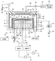
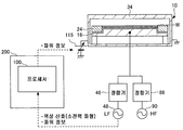
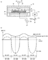
도 1a는 일 실시형태에 따른 플라즈마 처리 장치(1)의 일례를 도시한 도면이다. 본 실시형태에 따른 플라즈마 처리 장치(1)는, 용량 결합형의 평행 평판 플라즈마 처리 장치이고, 예컨대 표면이 양극 산화 처리된 알루미늄이나 용사된 산화이트륨(Y2O3)을 포함하는 원통형의 처리 용기(10)를 갖고 있다. 처리 용기(10)는 접지되어 있다.1A is a diagram showing an example of a
처리 용기(10)의 바닥부에는, 세라믹스 등을 포함하는 절연판(12)을 통해 원기둥형의 지지대(14)가 배치되고, 이 지지대(14) 위에 예컨대 알루미늄을 포함하는 배치대(16)가 설치되어 있다. 배치대(16)는 하부 전극을 구성하고, 그 위에 피처리체의 일례인 웨이퍼(W)가 배치된다.At the bottom of the
배치대(16)의 상면에는, 웨이퍼(W)를 정전력으로 흡착 유지하는 정전 척(20)이 설치되어 있다. 정전 척(20)은, 도전막을 포함하는 전극(20a)을 절연층(20b) 사이에 끼운 구조를 갖고, 전극(20a)에는 직류 전원(22)이 접속되어 있다. 그리고, 직류 전원(22)으로부터의 직류 전압에 의해 발생한 쿨롱력 등의 정전력에 의해 웨이퍼(W)가 정전 척(20)에 흡착 유지된다.On the upper surface of the placing table 16, an
배치대(16) 상이며 웨이퍼(W)의 둘레 가장자리에는, 예컨대 실리콘을 포함하는 도전성의 에지 링(24)이 배치되어 있다. 배치대(16) 및 지지대(14)의 외주 측면에는, 예컨대 석영을 포함하는 원통형의 내벽 부재(26)가 설치되어 있다. 에지 링(24)의 외주 측면에는 인슐레이터 링(25)이 설치되어 있다.A
지지대(14)의 내부에는, 예컨대 원주 상에 냉매실(28)이 형성되어 있다. 냉매실(28)에는, 외부에 설치된 칠러 유닛으로부터 배관(30a, 30b)을 통해 미리 정해진 온도의 냉매, 예컨대 냉각수가 순환 공급되고, 냉매의 온도에 의해 배치대(16) 상의 웨이퍼(W)의 처리 온도가 제어된다. 또한, 전열 가스 공급 기구로부터의 전열 가스, 예컨대 He 가스가 가스 공급 라인(32)을 통해 정전 척(20)의 상면과 웨이퍼(W)의 이면 사이에 공급된다.Inside the
배치대(16)의 상방에는, 배치대(16)와 대향하여 상부 전극(34)이 설치되어 있다. 상부 전극(34)과 하부 전극 사이는 플라즈마 처리 공간이 된다. 상부 전극(34)은, 배치대(16) 상의 웨이퍼(W)와 대향하여 플라즈마 처리 공간과 접하는 면, 즉 대향면을 형성한다.The
상부 전극(34)은, 절연성의 차폐 부재(42)를 통해, 처리 용기(10)의 상부에 지지되어 있다. 상부 전극(34)은, 배치대(16)와의 대향면을 구성하고 또한 다수의 가스 토출 구멍(37)을 갖는 전극판(36)과, 이 전극판(36)을 착탈 가능하게 지지하며, 도전성 재료, 예컨대 표면이 양극 산화 처리된 알루미늄을 포함하는 전극 지지체(38)를 갖는다. 전극판(36)은, 실리콘이나 SiC로 구성되는 것이 바람직하다. 전극 지지체(38)의 내부에는, 가스 확산실(40)이 형성되고, 이 가스 확산실(40)로부터는 가스 토출 구멍(37)에 연통(連通)되는 다수의 가스 통류 구멍(41)이 하방으로 연장되어 있다.The
전극 지지체(38)에는, 가스 확산실(40)로 처리 가스를 유도하는 가스 도입구(62)가 형성되어 있고, 이 가스 도입구(62)에는 가스 공급관(64)이 접속되며, 가스 공급관(64)에는 처리 가스 공급원(66)이 접속되어 있다. 가스 공급관(64)에는, 상류측으로부터 순서대로 매스 플로우 컨트롤러(MFC)(68) 및 개폐 밸브(70)가 설치되어 있다. 그리고, 처리 가스 공급원(66)으로부터, 에칭을 위한 처리 가스가 가스 공급관(64)으로부터 가스 확산실(40)에 이르고, 가스 통류 구멍(41)을 통해 가스 토출 구멍(37)으로부터 샤워형으로 플라즈마 처리 공간에 토출된다. 이와 같이 하여 상부 전극(34)은 처리 가스를 공급하기 위한 샤워 헤드로서 기능한다.The
에지 링(24)에는, 가변 직류 전원(50)이 전기적으로 접속되고, 가변 직류 전원(50)으로부터 직류 전압이 인가된다. 가변 직류 전원(50)으로부터 공급되는 직류 전압 및 직류 전류의 극성 및 전류·전압과, 이들을 온·오프하는 전자 스위치의 제어는, 제어부(200)에 의해 행해진다. 가변 직류 전원(50)에는, LF 및 HF 전류를 커트하고, 가변 직류 전원(50)을 보호하는 로우패스 필터(51)가 접속되어 있다.The variable
디포지션 실드(11)에는, 가변 직류 전원(115)이 전기적으로 접속되고, 가변 직류 전원(115)으로부터 직류 전압이 인가된다. 가변 직류 전원(115)으로부터 공급되는 직류 전압 및 직류 전류의 극성, 및 직류 전압 및 직류 전류와 이들을 온·오프하는 전자 스위치의 제어는, 제어부(200)에 의해 행해진다. 가변 직류 전원(115)에는, LF 및 HF 전류를 커트하고, 가변 직류 전원(115)을 보호하는 로우패스 필터(116)가 접속되어 있다. 본 실시형태에서는, 가변 직류 전원(115)은 디포지션 실드(11)에 접속되어 있으나, 이것에 한정되지 않고, 처리 용기(10) 내의 파트, 예컨대 처리 용기(10)의 천장벽, 인슐레이터 링(25) 및 배플판(83) 중 적어도 어느 하나의 파트에 접속되어도 좋다. 또한, 가변 직류 전원(115)은, 배치대(16)와 대향하는 상부 전극(34)의 하방에 형성된 처리 공간 혹은 가스 공간, 또는 에지 링(24)의 상공 외측에 배치된 전용의 파트에 접속되어도 좋다. 또한, 가변 직류 전원(115)은, 하나에 한정되지 않고, 2개 이상이 디포지션 실드(11)나 천장벽 등의 적어도 어느 하나의 파트에 접속되어도 좋다. 도 1에는, 일례로서, 에지 링(24)의 상방의 외측에 전용의 파트(101)가 배치되어 있다. 파트(101)는 내부에 전극을 갖고, 가변 직류 전원(104)이 전기적으로 접속되며, 가변 직류 전원(104)으로부터 그 전극에 직류 전압이 인가된다. 가변 직류 전원(104)에는, LF 및 HF 전류를 커트하고, 또한, 가변 직류 전원(104)을 보호하는 로우패스 필터(103)가 접속되어 있다. 파트(101)는, 링형이어도 좋고, 원호형이어도 좋으며, 그 외의 형상이어도 좋다. 파트(101)는, 예컨대, 실리콘(Si)이나 실리콘 카바이드(SiC)로 구성된다.The variable
배치대(16)에는, 급전봉(47) 및 정합기(46)를 통해 제1 고주파 전원(48)이 접속되어 있다. 제1 고주파 전원(48)은, 배치대(16)에 LF 전력을 인가한다. 이에 의해, 배치대(16) 상의 웨이퍼(W)에 이온이 인입된다. 제1 고주파 전원(48)은, 200 ㎑∼13.56 ㎒의 범위 내의 주파수의 고주파 전력을 출력한다. 정합기(46)는 제1 고주파 전원(48)의 내부 임피던스와 부하 임피던스를 정합시킨다.The first high-
배치대(16)에는, 급전봉(89) 및 정합기(88)를 통해 제2 고주파 전원(90)이 접속되어 있다. 제2 고주파 전원(90)은, 배치대(16)에 HF 전력을 인가한다. HF의 주파수는, 13.56 ㎒ 이상, 예컨대 100 ㎒여도 좋다. LF의 주파수는 HF의 주파수보다 낮으며, 예컨대 400 ㎑여도 좋다. 정합기(88)는, 제2 고주파 전원(90)의 내부 임피던스와 부하 임피던스를 정합시킨다. 배치대(16)에는, 미리 정해진 고주파를 접지에 통과시키기 위한 필터가 접속되어도 좋다. 한편, 제2 고주파 전원(90)으로부터 공급되는 HF 전력을, 상부 전극(34)에 인가해도 좋다.A second high-
처리 용기(10)의 바닥부에는 배기구(80)가 형성되고, 이 배기구(80)에 배기관(82)을 통해 배기 장치(84)가 접속되어 있다. 배기 장치(84)는, 터보 분자 펌프 등의 진공 펌프를 갖고 있고, 처리 용기(10) 내부를 원하는 진공도까지 감압할 수 있다. 또한, 처리 용기(10)의 측벽에는 웨이퍼(W)의 반입 반출구(85)가 형성되어 있고, 이 반입 반출구(85)는 게이트 밸브(86)에 의해 개폐 가능하다. 또한, 처리 용기(10)의 내벽을 따라 에칭 시에 생성된 부생성물(디포지션)이 부착되는 것을 방지하기 위한 디포지션 실드(11)가 착탈 가능하게 설치되어 있다. 즉, 디포지션 실드(11)가 처리 용기의 벽부를 구성하고 있다. 또한, 디포지션 실드(11)는, 내벽 부재(26)의 외주에도 설치되어 있다. 처리 용기(10)의 바닥부의 처리 용기벽측의 디포지션 실드(11)와 내벽 부재(26)측의 디포지션 실드(11) 사이에는 배플판(83)이 설치되어 있다. 디포지션 실드(11) 및 배플판(83)으로서는, 알루미늄재에 Y2O3 등의 세라믹스를 피복한 것을 이용할 수 있다.An exhaust port 80 is formed at the bottom of the
이러한 구성의 플라즈마 처리 장치에 있어서 에칭 처리를 행할 때에는, 먼저, 게이트 밸브(86)를 개방 상태로 하여, 반입 반출구(85)를 통해 에칭 대상 웨이퍼(W)를 처리 용기(10) 내에 반입하고, 배치대(16) 상에 배치한다. 그리고, 처리 가스 공급원(66)으로부터 에칭을 위한 처리 가스를 미리 정해진 유량으로 가스 확산실(40)에 공급하고, 가스 통류 구멍(41) 및 가스 토출 구멍(37)을 통해 처리 용기(10) 내에 공급한다. 또한, 배기 장치(84)에 의해 처리 용기(10) 내부를 배기하고, 그 안의 압력을 예컨대 0.1 ㎩∼150 ㎩의 범위 내의 설정값으로 한다. 여기서, 처리 가스로서는, 종래 이용되고 있는 여러 가지의 것을 채용할 수 있고, 예컨대 C4F8 가스와 같은 플루오로카본 가스(CxFy)로 대표되는 할로겐 원소를 함유하는 가스를 적합하게 이용할 수 있다. 또한, Ar 가스나 O2 가스 등의 다른 가스가 포함되어 있어도 좋다.When performing an etching process in the plasma processing apparatus having such a configuration, first, the
이와 같이 처리 용기(10) 내에 에칭 가스를 도입한 상태에서, 제2 고주파 전원(90)으로부터 HF 전력을 배치대(16)에 인가한다. 또한, 제1 고주파 전원(48)으로부터 LF 전력을 배치대(16)에 인가한다. 또한, 직류 전원(22)으로부터 직류 전압을 전극(20a)에 인가하여, 웨이퍼(W)를 배치대(16)에 유지한다. 또한, 가변 직류 전원(50)으로부터 직류 전압을 에지 링(24)에 인가한다.As described above, in the state where the etching gas is introduced into the
상부 전극(34)의 가스 토출 구멍(37)으로부터 토출된 처리 가스는, 주로 HF 전력에 의해 해리 및 전리하여 플라즈마가 생성된다. 플라즈마 중의 라디칼이나 이온에 의해 웨이퍼(W)의 피처리면이 에칭된다. 또한, 배치대(16)에 LF 전력을 인가함으로써, 플라즈마 중의 이온을 제어하여, 고애스펙트비의 홀의 에칭을 가능하게 하는 등, 플라즈마의 제어 마진을 넓게 할 수 있다.The processing gas discharged from the
플라즈마 처리 장치(1)에는, 장치 전체의 동작을 제어하는 제어부(200)가 설치되어 있다. 제어부(200)는, ROM(Read Only Memory) 및 RAM(Random Access Memory) 등의 메모리에 저장된 프로세스 레시피에 따라, 에칭 등의 원하는 플라즈마 처리를 실행한다. 프로세스 레시피에는, 프로세스 조건에 대한 장치의 제어 정보인 프로세스 시간, 압력(가스의 배기), 고주파 전력이나 전압, 각종 가스 유량이 설정되어도 좋다. 또한, 프로세스 레시피에는, 처리 용기 내 온도[상부 전극 온도, 처리 용기의 측벽 온도, 웨이퍼(W) 온도, 정전 척 온도 등], 칠러로부터 출력되는 냉매의 온도 등이 설정되어도 좋다. 한편, 이들 프로그램이나 처리 조건을 나타내는 프로세스 레시피는, 하드 디스크나 반도체 메모리에 기억되어도 좋다. 또한, 프로세스 레시피는, CD-ROM, DVD 등의 가반성(可搬性)의 컴퓨터 판독 가능한 기억 매체에 수용된 상태로 미리 정해진 위치에 세팅되어, 판독되도록 해도 좋다.The
예컨대, 제어부(200)는, 가변 직류 전원(115)으로부터 출력되는 직류 전압(직류 전압)을, 바이어스 파워의 전달 경로에서 측정되는, 전압, 전류, 전자계, 발생한 플라즈마의 발광 주기 또는 웨이퍼(W)(하부 전극) 상의 플라즈마의 시스 두께의 변화(이하, 「주기적으로 변동하는 파라미터」라고도 함)의 각 주기 내의 부분 기간에 인가하여, 직류 전압의 온과 오프나 그 전압의 대소를 교대로 반복하도록 제어해도 좋다. 제어부(200)는, 바이어스 파워의 고주파의 주기 혹은 바이어스 파워의 펄스파(이하, 「DC 펄스」라고도 함)의 주기에 동기하는 신호에 의해, 직류 전압의 온과 오프나 그 전압의 대소를 교대로 반복하도록 제어해도 좋다.For example, the
바이어스 파워의 전달 경로란, 제1 고주파 전원(48)→정합기(46)→급전봉(47)→배치대(16)→플라즈마→상부 전극(34)→(접지)를 말한다. 바이어스 파워의 전달 경로에서 측정되는 전압, 전류, 전자계란, 제1 고주파 전원(48)으로부터 정합기(46)의 내부 및 급전봉(47)을 통해 배치대(16)에 이르기까지의 파트와 상부 전극(34)에서 측정되는 전압, 전류, 전자계, 또는 플라즈마에서 측정되는 전자계를 말한다.The transmission path of the bias power refers to the first high-
직류 전압은, 후술하는 제1 상태와 제2 상태를 주기적으로 반복하여, 제1 상태는, 주기적으로 변동하는 파라미터의 각 주기 내의 부분 기간에 제1 전압값을 인가하고, 제2 상태는, 제1 상태와 연속해서 제2 전압값을 인가하도록 제어된다. 직류 전압이, 제1 상태와, 제2 상태와, 2개 이상의 전압값을 갖는 2 이상의 상태를 주기적으로 반복하여, 파라미터의 각 주기 내의 부분 기간에 제1 전압값을 인가하고, 제1 상태와 제2 상태와 2 이상의 상태가 연속되도록 제2 전압값과 2개 이상의 전압값을 순서대로 인가해도 좋다. 「주기적으로 변동하는 파라미터」는, 주기적으로 변동하는 전극 전위의 일례이다.The DC voltage periodically repeats the first state and the second state, which will be described later, and the first state applies a first voltage value to a partial period within each cycle of the parameter that fluctuates periodically, and the second state is It is controlled to apply the second voltage value continuously with the 1 state. The DC voltage periodically repeats the first state, the second state, and two or more states having two or more voltage values to apply a first voltage value to a partial period within each period of the parameter, and the first state and The second voltage value and the two or more voltage values may be sequentially applied so that the second state and the two or more states are continuous. The "periodically variable parameter" is an example of an periodically changing electrode potential.
주기적으로 변동하는 파라미터는, 배치대(16)로부터 급전봉(47)을 통해 접속되는 정합기의 내부까지의 어느 하나의 부재에 있어서 측정되는 전압, 전류 또는 전자계 중 어느 하나인 것이 바람직하다.It is preferable that the parameter that fluctuates periodically is any one of a voltage, current, or electromagnetic field measured in any member from the placing table 16 to the inside of the matcher connected through the feeding
바이어스 파워의 전달 경로에서 주기적으로 변동하는 파라미터를 측정하는 방법으로서는, 바이어스 파워의 전달 경로의 어느 하나의 파트 근방에 전압 센서, 전류 센서 또는 BZ 센서(유도 자기장을 측정하는 센서)를 설치함으로써 각 파트의 전압, 전류 또는 유도 자기장을 계측하는 방법을 일례로서 들 수 있다. 한편, 도 2에는, 전압 센서(300)를 도시하였으나, 이것에 한정되지 않고, 전류 센서 또는 BZ 센서여도 좋다. 또한, 상기 각 센서의 배치는, 급전봉(47)에 접속되는 것이 바람직하지만, 이것에 한정되지 않는다. 전압 센서(300) 등의 센서로부터의 신호는, 예컨대 제어부(200)의 신호 발생 회로(102)에 입력된다.As a method of measuring a parameter that fluctuates periodically in the transmission path of a bias power, each part is provided by installing a voltage sensor, a current sensor, or a BZ sensor (a sensor that measures an inductive magnetic field) near any part of the transmission path of the bias power. A method of measuring the voltage, current, or induced magnetic field of the is exemplified. Meanwhile, although the
또한, 플라즈마의 발광 주기, 웨이퍼(W) 상의 플라즈마의 시스 두께의 변화의 주기를 지표로 해도 좋다. 플라즈마의 발광 주기는, 포토다이오드, 포토마이크로 센서, 포토멀티플라이어 등의 광전 변환 소자로 검출할 수 있다. 시스 두께에 대해서는, ICCD 카메라 등을 이용하여 나노 sec의 간격(예컨대 10 nsec∼250 nsec)으로 셔터를 눌러, 이에 의해, 시스 두께의 변화를 측정할 수 있다. 예컨대, 가변 직류 전원(115)으로부터 출력되는 직류 전압을 LF 전압의 주기에 동기시키도록 제어해도 좋다. 이에 의해, 이온의 충돌 에너지를 제어할 수 있다. 또한, 클리닝 처리의 효율화를 도모할 수 있다.Further, the light emission cycle of the plasma and the change cycle of the sheath thickness of the plasma on the wafer W may be used as indicators. The light emission cycle of the plasma can be detected by photoelectric conversion elements such as photodiodes, photomicro sensors, and photomultipliers. As for the sheath thickness, a change in sheath thickness can be measured by pressing the shutter at an interval of nanoseconds (for example, 10 nsec to 250 nsec) using an ICCD camera or the like. For example, the DC voltage output from the variable
한편, 배치대(16)는, 웨이퍼(W)를 배치하는 전극(제1 전극)의 일례이다. 상부 전극은, 배치대(16)와 대향하는 전극(제2 전극)의 일례이다. 제1 고주파 전원(48)은, 배치대(16)에 LF 전력(바이어스 파워)을 공급하는 바이어스 전원의 일례이다. 제2 고주파 전원(90)은, 배치대(16) 또는 상부 전극(34)에 LF 전력보다 높은 주파수의 소스 파워를 공급하는 소스 전원의 일례이다. 가변 직류 전원(115)은, 처리 용기(10) 내의 플라즈마에 폭로(暴露)되는 파트에 전압을 공급하는 전원의 일례이다. 가변 직류 전원(115)은, 직류 전원이어도 좋다. 제어부(200)는, 바이어스 전원, 소스 전원 및 직류 전원을 제어하는 제어부의 일례이다. 바이어스 파워를 인가하는 하부 전극[배치대(16)]의 전위를, 전극 전위라고도 한다.On the other hand, the placing table 16 is an example of an electrode (first electrode) on which the wafer W is placed. The upper electrode is an example of an electrode (second electrode) facing the placing table 16. The first high
한편, 도 1의 플라즈마 처리 장치(1)에서는, 디포지션 실드(11)에 가변 직류 전원(115)이 전기적으로 접속되고, 가변 직류 전원(115)으로부터 직류 전압이 인가되었으나, 이것에 한정되지 않는다. 가변 직류 전원(115)이, 처리 용기(10) 내의 파트, 예컨대 처리 용기(10)의 천장벽, 인슐레이터 링(25) 및 배플판(83) 중 적어도 어느 하나의 파트에 접속되고, 이들 파트 중 적어도 어느 하나에 직류 전압을 인가해도 좋다. 또한, 가변 직류 전원(115)이, 배치대(16)와 대향하는 상부 전극(34)의 하방에 형성된 처리 공간 혹은 가스 공간, 또는 에지 링(24)의 상공 외측에 배치된 전용의 파트에 접속되고, 이 전용의 파트에 직류 전압을 인가해도 좋다.On the other hand, in the
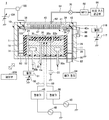
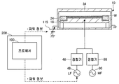
도 1b는 일 실시형태에 따른 플라즈마 처리 장치(1)의 다른 예를 도시한 도면이다. 도 1b에서는, 차폐 부재(42)의 내부에 전극(42a)이 설치되어 있다. 전극(42a)에는, 가변 직류 전원(117)이 전기적으로 접속되고, 가변 직류 전원(117)으로부터 직류 전압이 인가된다. 가변 직류 전원(117)에는, LF 및 HF 전류를 커트하고, 가변 직류 전원(117)을 보호하는 로우패스 필터(118)가 접속되어 있다.1B is a diagram showing another example of the
또한, 가변 직류 전원(115)은, 하나에 한정되지 않고, 2개 이상이 디포지션 실드나 천장벽 등의 적어도 어느 하나의 파트에 접속되어도 좋다. 도 1a에는, 일례로서, 에지 링(24)의 상방의 외측에 전용의 파트(101)가 배치되어 있다. 파트(101)는 내부에 전극을 갖고, 가변 직류 전원(104)이 전기적으로 접속되며, 가변 직류 전원(104)으로부터 그 전극에 직류 전압이 인가된다. 가변 직류 전원(104)에는, LF 및 HF 전류를 커트하고, 또한, 가변 직류 전원(104)을 보호하는 로우패스 필터(103)가 접속되어 있다. 파트(101)는, 링형이어도 좋고, 원호형이어도 좋으며, 그 외의 형상이어도 좋다. 파트(101)는, 예컨대, 실리콘(Si)이나 실리콘 카바이드(SiC)로 구성된다.Further, the variable
[제어부의 구성][Configuration of control part]
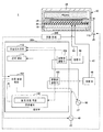
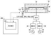
제어부(200)의 구체적 구성에 대해, 도 2를 참조하여 설명한다. 제어부(200)는, 프로세서(100), 신호 발생 회로(102), 방향성 결합기(105, 108), 전력 미터(111), 오실로스코프(112)를 갖는다. 단, 전력 미터(111), 오실로스코프(112), 방향성 결합기(108)는 설치하지 않아도 좋다.The specific configuration of the
제1 고주파 전원(48)의 급전 라인에는, 제1 고주파 전원(48)과 정합기(46) 사이에 방향성 결합기(105)가 접속되어 있다. 제2 고주파 전원(90)의 급전 라인에는, 제2 고주파 전원(90)과 정합기(88) 사이에 방향성 결합기(108)가 접속되어 있다.A
방향성 결합기(105)는, LF의 진행파 파워의 일부를 오실로스코프(112)에 부여한다. 방향성 결합기(108)는, HF의 진행파 파워의 일부를 오실로스코프(112)에 부여한다. 일 실시형태에 있어서, 오실로스코프(112)에 표시되는 LF의 주파수는, 예컨대 400 ㎑이고, HF의 주파수는, 예컨대 100 ㎒이다. 이에 의해, 오실로스코프(112)에서는, LF의 진행파의 파형과 HF의 진행파의 파형을 관찰할 수 있다.The
방향성 결합기(108)는, HF의 진행파의 일부를 전력 미터(111)에 부여한다. 전력 미터(111)는, HF의 진행파의 전력량을 계량한다.The
방향성 결합기(105)는, LF의 진행파의 일부를 프로세서(100)에 부여한다. 프로세서(100)는, LF의 진행파에 동기시키는 DC용(가변 직류 전원용)의 동기 신호를 작성한다. 예컨대, 프로세서(100)는, LF의 진행파의 정(正; positive)의 타이밍에 동기시켜 DC용의 동기 신호를 작성해도 좋다. 한편, 방향성 결합기(105) 대신에, 상기 센서를 이용하여 검출한 LF 전력을 프로세서(100)에 부여해도 좋다.The
프로세서(100)는, 작성한 동기 신호를 신호 발생 회로(102)에 부여한다. 신호 발생 회로(102)는, 부여된 동기 신호로부터 LF의 진행파에 동기하는 제어 신호를 생성해서, 가변 직류 전원(115) 및 제1 고주파 전원(48)에 부여한다.The
제어 신호의 생성 방법에는, 이하의 2가지가 있다. 제1 고주파 전원(48)이 일반적인 전원인 경우, 방향성 결합기(105)가 제1 고주파 전원(48)으로부터 출력되는 LF 전력의 위상에 동기하는 파형을 취출하여, 프로세서(100)에 입력한다. 단, 이것에 한정되지 않고, 프로세서(100)가, 제1 고주파 전원(48)으로부터 직접, LF 전력의 위상에 동기하는 파형을 입력해도 좋다. LF 전력의 위상에 동기하는 파형, LF 전압 또는 LF 전류의 위상에 동기하는 파형, 및 DC 펄스의 전력, 전압 또는 전류의 위상에 동기하는 파형을 이하, 바이어스 파형이라고도 한다. DC 펄스는, LF 전압의 피크에 대응하는 펄스형의 전압을 말한다. 원하는 파형의 바이어스 파워는, 바이어스 파형의 LF 파워에 상당한다.There are two methods for generating a control signal. When the first high-
프로세서(100)는, 입력된 파형의 신호에 동기시켜 또는 상기 신호로부터 임의의 지연과 임의의 폭을 갖는 온 신호를 작성하여, 신호 발생 회로(102)에 송신한다. 프로세서(100)는, 제1 고주파 전원(48)으로부터 LF 전력의 위상에 동기하는 파형을 입력하지 않고, 제1 고주파 전원(48)을 제어하기 위한 LF의 신호를 스스로 생성하고, 그 LF의 신호에 동기시켜 또는 상기 신호로부터 임의의 지연과 임의의 폭을 갖는 온 신호를 작성해도 좋다. 온 신호는, 동기 신호의 일례이다.The
신호 발생 회로(102)는, 온 신호 동안, 직류 전압을 발생시키기 위해서 가변 직류 전원(115)에 지령 신호를 보낸다. 지령 신호에는, 가변 직류 전원(115)의 입력 형태에 따라, 온 신호 동안, 직류 전압을 발생시키는 제어 신호 또는 온 신호 그 자체가 사용된다. 마찬가지로, 신호 발생 회로(102)는, 온 신호 동안, HF 전력을 발생시키기 위해서 지령 신호를 제2 고주파 전원(90)에 송신해도 좋다.The
제1 고주파 전원(48)이 LF 전력, 전압 또는 전류를 증폭하는 증폭기인 경우, 방향성 결합기(105)로부터의 신호는 사용하지 않고, 신호 발생 회로(102)가 제1 고주파 전원(48)으로부터 출력되는 LF 전력의 위상에 동기하는 파형 LF의 일부를 파형으로서 취출하고, 상기 파형의 신호로부터 임의의 지연과 임의의 폭을 갖는 온 신호를 작성해도 좋다. 신호 발생 회로(102)는, 상기 파형의 신호 및 온 신호를 가변 직류 전원(115)에 송신한다.When the first high
예컨대, 가변 직류 전원(115) 대신에 도시하지 않은 교류 전원을 구비하고, 교류 전원을 디포지션 실드 등의 파트에 전기적으로 접속하며, 제어(온) 신호에 기초하여 교류 전원으로부터 고주파 전압을 디포지션 실드 등의 파트에 인가해도 좋다. 가변 직류 전원(115) 및 교류 전원은, 파트에 원하는 파형의 전압을 공급하는 전원의 일례이다. 교류 전원은, 제2 고주파 전원(90)이어도 좋고, 다른 RF 전원이어도 좋다.For example, instead of the variable
또한, 도 3a에 도시된 바와 같이, 제1 고주파 전원(48)으로부터 출력되는 LF 전력의 위상에 동기하는 파형을 제어부(200)에 설치된 위상 시프트 회로(210)에 입력하고, 위상 시프트 회로(210)에서 LF의 위상을 미리 정해진 양만큼 시프트시킨 고주파 전압을 디포지션 실드 등의 파트에 인가해도 좋다.In addition, as shown in FIG. 3A, a waveform synchronized with the phase of the LF power output from the first high
위상 시프트 회로(210)에서 LF의 위상을 미리 정해진 양만큼 시프트하는 대신에, 제1 고주파 전원(48)으로부터 출력되는 LF의 파형으로부터 임의의 지연과 임의의 폭을 갖는 고주파 전압을 생성하고, 생성된 고주파 전압을 디포지션 실드 등의 파트에 인가해도 좋다.Instead of shifting the phase of the LF by a predetermined amount in the
단, 이상의 제어 신호의 생성 방법은 일례이며, 이것에 한정되지 않는다. 부여된 주기적으로 변동하는 파라미터의 각 주기 내의 부분 기간에 직류 전압과 고주파 전압 중 적어도 어느 하나를 인가하도록 제어하는 제어 신호를 생성할 수 있으면, 도 2에 도시된 제어부(200)의 회로에 한정되지 않고, 다른 하드웨어 또는 소프트웨어를 사용할 수 있다. 직류 전압의 경우, 예컨대, 온과 오프를 교대로 반복시키도록 제어하는 제어 신호를 생성해도 좋다.However, the above method of generating a control signal is an example and is not limited to this. If a control signal for controlling to apply at least one of a DC voltage and a high frequency voltage to a partial period within each period of the periodically fluctuating parameter is generated, it is not limited to the circuit of the
제1 고주파 전원(48)의 증폭기는, 400 ㎑의 LF의 변조 신호의 진폭(AM: ampl itude modulation)을 증폭하여, 하부 전극에 공급한다. 제2 고주파 전원(90)의 증폭기는, 100 ㎒의 HF의 변조 신호의 진폭을 증폭하여, 하부 전극에 공급한다.The amplifier of the first high
신호 발생 회로(102)는, 부여된 동기 신호로부터 바이어스 파워의 전달 경로에서 측정되는, 주기적으로 변동하는 파라미터의 각 주기 내의 부분 기간에 직류 전압을 인가하여, 직류 전압의 절대값이 High와 Low가 교대로 반복되도록 제어하는 제어 신호를 생성해서, 가변 직류 전원(115)에 부여해도 좋다. 프로세서(100)는, LF가 인가되어 있지 않은 경우, HF의 진행파의 정의 피크가 되는 타이밍에 동기시켜 DC용의 동기 신호를 작성해도 좋다.The
신호 발생 회로(102)는, 부여된 동기 신호로부터 바이어스 파워의 전달 경로에서 측정되는, 주기적으로 변동하는 파라미터의 각 주기 내의 부분 기간에 고주파 전압을 인가하여, 고주파 전압이 High와 Low가 교대로 반복되도록 제어하는 제어 신호를 생성해서, 가변 직류 전원(115)에 부여한다. 부분 기간은, 전극의 전위가 정의 피크가 되는 타이밍을 포함해도 좋고, 전극의 전위가 부(負; negative)의 피크가 되는 타이밍을 포함해도 좋으며, 그 양방의 타이밍을 포함해도 좋다. 예컨대, 도 3b 및 도 3c는 바이어스 파워의 전송 경로(급전계)에서 측정된 전압, 전류 또는 전자계 중 어느 하나를 「기준 전기 상태」로 하는 경우의 일례이다. 예컨대 도 3b에서는, 프로세서(100)가 전송 경로에 부착된 VI 프로브 등의 센서로부터 HF 전압 또는 전류, LF의 전압 또는 전류, HF의 위상 신호 또는 LF의 위상 신호 중 어느 하나를 입력으로 한다. 프로세서(100)는, 입력된 HF의 전압 또는 전류, LF의 전압 또는 전류, HF의 위상 신호 또는 LF의 위상 신호 중 어느 하나를 나타내는 기준 전기 상태의 1주기 내의 위상과 동기하여 직류 전압을 제1 상태와 제2 상태로 교대로 인가한다.The
프로세서(100)는, 센서로부터의 신호에 기초하지 않고서 제1 고주파 전원(48)으로부터 출력되는 바이어스 파워의 고주파 혹은 펄스파의 주기에 동기하는 신호를 이용하여 생성해도 좋다. 이 경우, 상기 신호의 상태를 기준 전기 상태로 할 수 있다. 또한, 바이어스 파워의 급전계에서 기준 전기 상태를 측정하는 공정을 생략할 수 있다. 예컨대 도 3c에서는, 프로세서(100)가, 제1 고주파 전원(48)으로부터 LF의 위상 신호(소전력 파형) 또는 바이어스 파워의 정보에 관한 신호를 입력으로 하고, 이 입력 신호에 기초하여 바이어스 파워의 고주파 혹은 펄스파의 주기에 동기하는 신호를 생성한다. 프로세서(100)는, 생성된 신호를 가변 직류 전원(115)에 출력한다. 가변 직류 전원(115)은, 이 신호에 기초하여 직류 전압을 제1 상태와 제2 상태로 교대로 인가한다.The
한편, 도 3d에 도시된 바와 같이, 프로세서(100)는, 제1 고주파 전원(48)으로부터의 신호를 이용하지 않고, 제1 고주파 전원(48)을 제어하기 위한 신호를 생성하고, 그 생성된 신호에 동기하는 신호를 생성함으로써, 제1 고주파 전원(48)으로부터 출력된 바이어스 파워의 고주파 혹은 펄스파의 주기에 동기하는 신호를 생성해도 좋다. 이 경우, 프로세서(100)는, 제1 고주파 전원(48)을 제어하는 LF의 신호를 생성하고, 이 생성된 신호에 동기하는 직류 전압의 신호를 생성한다. 프로세서(100)는, 생성된 LF의 신호를 제1 고주파 전원(48)에 송신하고, 생성된 직류 전압의 신호를 가변 직류 전원(115)에 송신한다. 제1 고주파 전원(48)은, LF의 신호에 기초하여 바이어스 파워를 출력한다. 가변 직류 전원(115)은, 직류 전압의 신호에 기초하여 직류 전압을 제1 상태와 제2 상태로 교대로 인가한다. 생성된 LF의 신호 및 직류 전압의 신호에는, 파워 정보가 포함된다.Meanwhile, as illustrated in FIG. 3D, the
[전극 전위와 이온의 충돌 에너지의 관계][Relationship between electrode potential and collision energy of ions]
다음으로, 전극 전위와 이온의 충돌 에너지의 관계에 대해 도 4를 참조하여 설명한다. 제1 고주파 전원(48)으로부터 정현파이며 LF 전력을 인가한 경우, LF 전압이 부일 때에는 LF 전압이 정일 때보다 자기 바이어스(Vdc)에 의해 전압이 부로 깊어진다. 이에 의해, 도 4에 도시된 바와 같이, LF 전력이 인가되는 전극 전위가 정일 때에는, 그 전극 전위가 측벽의 전위(접지)보다 높아진다. 플라즈마 전위는, 처리 용기(10) 내의 가장 높은 전위보다 약간 높은 전위를 취하기 때문에, 전극 전위가 정일 때에는 플라즈마 전위는 전극 전위보다 약간 높아진다. 그때의 플라즈마 전위와 측벽 전위의 전위차(Vb)를 도 4의 테두리(B) 내에 도시한다.Next, the relationship between the electrode potential and the collision energy of ions will be described with reference to FIG. 4. When LF power is applied, which is a sinusoidal wave from the first high
한편, LF 전력이 인가되는 전극 전위가 부일 때에는, 자기 바이어스(Vdc)에 의해 전극 전위가 측벽의 전위(접지)보다 낮아진다. 이때, 플라즈마 전위는 측벽의 전위보다 약간 높아진다. 그때의 플라즈마 전위와 측벽 전위의 전위차(Va)를 도 4의 테두리(A) 내에 도시한다. 이에 의해, 전극 전위가 정일 때의 플라즈마 전위와 측벽 전위의 전위차(Vb)는 전극 전위가 부일 때의 플라즈마 전위와 측벽 전위의 전위차(Va)보다 커진다. 이 때문에, 전극 전위가 정일 때, 측벽으로 향하는 이온의 가속 전압은 커져, 측벽에의 1개당의 이온의 충돌 에너지가 커진다. 이 결과, 측벽에의 스퍼터가 발생하기 쉬워진다. 따라서, 전극 전위에 따라 플라즈마 전위와 측벽 및 천장벽 전위의 전위차를 제어함으로써, 가속 전압을 제어하면 1개의 이온의 충돌 에너지를 제어할 수 있고, 측벽 및 천장벽에의 스퍼터력을 제어할 수 있다. 예컨대, 플라즈마 전위와 측벽 및 천장벽의 전위차를 크게 제어하면, 도 4의 (a)의 화살표로 나타내는 바와 같이, 측벽 및 천장벽에의 스퍼터력을 강하게 할 수 있다. 한편, 그 전위차를 작게 제어하면, 도 4의 (b)의 화살표로 나타내는 바와 같이, 측벽 및 천장벽에의 스퍼터력을 약하게 할 수 있다.On the other hand, when the electrode potential to which LF power is applied is negative, the electrode potential becomes lower than the potential (ground) of the side wall by self-bias (Vdc). At this time, the plasma potential is slightly higher than the potential of the side wall. The potential difference Va between the plasma potential and the sidewall potential at that time is shown in the rim A of FIG. 4. Thereby, the potential difference Vb between the plasma potential and the sidewall potential when the electrode potential is positive becomes larger than the potential difference Va between the plasma potential and the sidewall potential when the electrode potential is negative. For this reason, when the electrode potential is positive, the acceleration voltage of the ions directed to the sidewall increases, and the collision energy of ions per one sidewall increases. As a result, sputtering on the side walls is likely to occur. Therefore, by controlling the potential difference between the plasma potential and the sidewall and ceiling wall potentials according to the electrode potential, the collision energy of one ion can be controlled and the sputtering force to the sidewalls and ceiling walls can be controlled by controlling the acceleration voltage. . For example, if the electric potential difference between the plasma potential and the side wall and ceiling wall is largely controlled, the sputtering force to the side wall and ceiling wall can be strengthened, as indicated by the arrow in Fig. 4A. On the other hand, if the potential difference is controlled small, the sputtering force to the side walls and the ceiling walls can be weakened, as indicated by the arrow in Fig. 4B.
그래서, 일 실시형태에 따른 플라즈마 처리 장치(1)의 제어 방법에서는, 바이어스 파워를 하부 전극에 공급하고, 가변 직류 전원(115)으로부터의 직류 전압을 디포지션 실드(11) 등의 파트에 공급한다. 또한, 본 제어 방법은, 직류 전압이, 제1 전압값을 갖는 제1 상태와, 제1 전압값보다 높은 제2 전압값을 갖는 제2 상태를 주기적으로 반복하는 공정과, 전극의 전위의 각 주기 내의 부분 기간에 제1 전압값을 인가하고, 제1 상태와 제2 상태가 연속되도록 제2 전압값을 인가하는 공정을 갖는다. 직류 전압이, 제1 상태와, 제2 상태와, 2개 이상의 전압값을 갖는 2 이상의 상태를 주기적으로 반복하여, 전극의 전위의 각 주기 내의 부분 기간에 제1 전압값을 인가하고, 제1 상태와 제2 상태와 2 이상의 상태가 연속되도록 제2 전압값, 2개 이상의 전압값을 순서대로 인가하는 공정을 가져도 좋다. So, in the control method of the
제어부(200)는, 전극 전위의 주기와 동기하는 동기 신호를 작성하고, 상기 동기 신호로부터 직류 전압을 출력하는 직류 전원용의 제어 신호를 생성하여, 가변 직류 전원(115)과 위상 시프트 회로(210) 중 적어도 어느 하나에 송신한다. 전극의 전위의 주기란, 바이어스 파형의 주기에 동기한다. 이에 의해, 제어부(200)는, 가변 직류 전원(115)과 위상 시프트 회로(210) 중 적어도 어느 하나로부터 디포지션 실드(11) 등의 파트에 직류 전압을 공급한다. 예컨대, 직류 전압이, 제1 전압값을 갖는 제1 상태와, 상기 제1 전압값보다 높은 제2 전압값을 갖는 제2 상태를 주기적으로 반복하여, 상기 전극의 전위의 각 주기 내의 부분 기간에 상기 제1 전압값을 인가하고, 상기 제1 상태와 상기 제2 상태가 연속되도록 상기 제2 전압값을 인가하는 제1 제어 순서를 포함하는 프로그램을 갖는 기억 매체를 준비한다. 그리고, 제어부(200)는, 기억 매체의 프로그램을 실행한다. 이하에서는, 가변 직류 전원(115)에 직류 전압을 인가하는 경우를 예로 들어 설명한다.The
[DC 전압의 공급 타이밍][Supply timing of DC voltage]
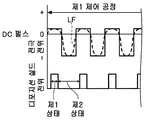
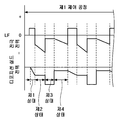
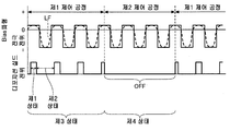
본 실시형태에 있어서의 DC 전압의 공급 타이밍의 효과에 대해, 도 5를 참조하면서 설명한다. 도 5는 일 실시형태에 따른 직류 전압의 인가 방법(스퍼터 제어)과 그 효과의 일례를 도시한 도면이다. 이하에서는, LF 전압 및 DC 전압을 제어했을 때의, LF 전압을 인가한 전극 전위와 플라즈마 전위, 디포지션 실드(11)의 전위에 대해 설명한다.The effect of the timing of supplying the DC voltage in this embodiment will be described with reference to FIG. 5. 5 is a diagram showing an example of a method of applying a DC voltage (sputter control) and its effect according to an embodiment. Hereinafter, the electrode potential, plasma potential, and potential of the
(스퍼터 억제)(Sputter suppression)
도 5의 (b)의 횡축에는 시간이 나타나고, 종축에는 LF 전압을 공급했을 때의 전극 전위, 플라즈마 전위, 디포지션 실드(11)의 전위가 나타나 있다. 전극 전위는, LF 전압과 거의 동일하다. 도 5의 (b)의 C의 테두리 내에 도시된 바와 같이, LF 전압이 정일 때에는 가변 직류 전원(115)으로부터 정의 직류 전압이 디포지션 실드(11)에 인가된다. 이에 의해, 플라즈마 전위와 디포지션 실드(11)의 전위차를 작게 할 수 있고, 도 5의 (a)에 화살표로 나타내는 바와 같이 측벽에의 스퍼터력을 억제할 수 있다.Time is shown in the horizontal axis of Fig. 5B, and the potential of the electrode potential, the plasma potential, and the
도 5의 (b)에 도시된 바와 같이, LF 전압이 부일 때에는 가변 직류 전원(115)으로부터의 직류 전압의 인가는 정지되어, 디포지션 실드(11)에 인가되는 직류 전압은 0이 된다. 직류 전압은, 전극 전위가 정인 타이밍에 일치시킨 구형파(矩形波)뿐만이 아니라, 상승의 슬로우 업 또는 하강의 슬로우 다운 중 적어도 어느 하나를 포함하는 대략 구형파를 인가해도 좋다.As shown in Fig. 5B, when the LF voltage is negative, the application of the DC voltage from the variable
제어부(200)는, 전극 전위의 주기와 동기하는 동기 신호로부터 LF 전압이 정일 때에 정의 직류 전압을 인가하고, LF 전압이 부일 때에 직류 전압의 인가를 정지하는 직류 전원용의 제어 신호를 생성하여, 가변 직류 전원(115)에 송신한다. LF 전압이 정일 때에 정의 직류 전압을 인가하는 상태는 제1 상태의 일례이고, LF 전압이 부일 때에 직류 전압의 인가를 정지하는 상태는 제2 상태의 일례이다. 제어 신호를 수신하면, 가변 직류 전원(115)은, 직류 전압의 제1 상태와 제2 상태를 전극 전위의 주기와 동기하여 교대로 인가한다.The
LF 전력이 인가되는 전극 전위가 부일 때에는 가변 직류 전원(115)으로부터의 직류 전압의 인가는 정지되고, 플라즈마 전위와 디포지션 실드(11)의 전위차(Voff)가, 측벽으로 향하는 이온을 가속하는 가속 전압이 된다. 따라서, 측벽에의 1개당의 이온의 충돌 에너지는 전위차(Voff)에 의해 정해진다.When the electrode potential to which LF power is applied is negative, the application of the DC voltage from the variable
한편, 도 5의 (b)의 테두리(C) 내에 도시된 전극 전위가 정일 때에는, 가변 직류 전원(115)으로부터의 직류 전압은 온되어, 정의 직류 전압이 디포지션 실드(11)에 인가된다. 그러면, 플라즈마 전위와 디포지션 실드(11)의 전위차(Vc)가 가속 전압이 되고, 측벽에의 1개당의 이온의 충돌 에너지는 전위차(Vc)에 의해 정해진다. 플라즈마 전위와 디포지션 실드(11)의 전위차(Vc)는, 가변 직류 전원(115)으로부터의 정의 직류 전압이 디포지션 실드(11)에 인가되지 않는 경우와 비교하여 작아진다. 이 때문에, 측벽에의 1개당의 이온의 충돌 에너지는, 정의 직류 전압이 디포지션 실드(11)에 인가된 경우, 인가되지 않는 경우와 비교하여 낮아진다. 이와 같이, 전극의 전위가 부일 때에는 플라즈마 전위와 디포지션 실드(11)의 전위차(Voff)는 작다. 이에 대해, 가변 직류 전원(115)으로부터의 정의 직류 전압을 온하지 않으면, 전극의 전위가 정일 때에는 전극 전위가 벽의 전위보다 커지기 때문에 플라즈마 전위와 디포지션 실드(11)의 전위차가 크다. 이 때문에, 가변 직류 전원(115)으로부터의 정의 직류 전압을 온하여, 플라즈마 전위와 디포지션 실드(11)의 전위차를 작게 하도록 제어함으로써, 측벽에의 스퍼터력을 억제할 수 있다. 이에 의해, 처리 용기(10) 내의 하부 전극과 비교하여 측벽의 면적을 크게 함으로써, 캐소드/애노드비를 제어하여, 단위 면적당의 1개의 이온의 충돌 에너지를 작게 보이게 하는 제어와 동일한 제어가 가능해진다. 이에 의해, 단위 면적당의 1개의 이온의 충돌 에너지를 작게 함으로써, 측벽에의 스퍼터에 의한 프로세스에의 영향을 작게 할 수 있다. 한편, 제1 상태와 제2 상태는, 가변 직류 전원(115)으로부터의 정의 직류 전압을 온·오프함으로써 설정하는 제어에 한정되지 않는다. 제1 상태와 제2 상태는, 가변 직류 전원(115)으로부터의 정의 직류 전압을 High·Low로 함으로써 설정하도록 제어해도 좋다.On the other hand, when the electrode potential shown in the rim C of FIG. 5B is positive, the DC voltage from the variable
측벽에의 이온의 충돌 에너지를 줄이고 싶은 경우, 전극 전위가 정일 때에 디포지션 실드(11)에 정의 직류 전압을 온으로 제어함으로써, 전극 전위가 정일 때에 이온이 측벽과 충돌하는 효과를 저감할 수 있다. 이와 같이 하여 측벽에의 이온 충돌 에너지를 억제함으로써 챔버의 측면의 수명을 연장시킬 수 있다. 또한, 측벽에의 이온 충돌 에너지를 억제함으로써 파티클을 저감할 수 있다. 또한, 측벽에의 이온 충돌 에너지를 억제함으로써, 클리닝 사이클을 연장시킬 수 있다.When it is desired to reduce the collision energy of ions on the side wall, the positive DC voltage is turned on to the
또한, 전극 전위가 부일 때에 정의 직류 전압을 오프로 제어함으로써, 전극 전위가 부일 때에 이온이 웨이퍼(W)와 충돌하는 에너지를 유지할 수 있다.Further, by controlling the positive direct-current voltage to OFF when the electrode potential is negative, it is possible to maintain energy in which ions collide with the wafer W when the electrode potential is negative.
(클리닝/특정 프로세스)(Cleaning/specific process)
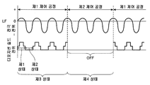
이상으로 설명한 제1 상태의 기간은, 전극 전위가 정의 피크가 되는 타이밍을 포함하고, 정 또는 부의 직류 전압을 상기 파트에 인가해도 좋다. 제1 상태의 기간은, 전극 전위가 부의 피크가 되는 타이밍을 포함하고, 정 또는 부의 직류 전압을 상기 파트에 인가해도 좋다.The period of the first state described above includes the timing at which the electrode potential becomes a positive peak, and a positive or negative DC voltage may be applied to the part. The period in the first state includes the timing at which the electrode potential becomes a negative peak, and a positive or negative DC voltage may be applied to the part.
도 6은 일 실시형태에 따른 전극 전위의 정부와 이온의 충돌 에너지의 일례를 도시한 도면이다. 도 6의 (c)의 테두리(H) 내에 도시된 바와 같이, 예컨대, 전극 전위가 정일 때에 정의 직류 전압을 디포지션 실드(11) 및 천장벽[예컨대, 차폐 부재(42)]에 인가한 경우, 플라즈마 전위와 디포지션 실드(11)의 전위의 전위차가 H1로부터 H2로 작아져, 측벽에의 1개당의 이온의 충돌 에너지가 낮아진다. 그 결과, 측벽 및 천장벽에의 스퍼터력을 약하게 할 수 있다. 한편, 전극 전위가 정일 때에 부의 직류 전압을 디포지션 실드(11) 및 천장벽에 인가한 경우, 플라즈마 전위와 디포지션 실드(11)의 전위의 전위차가 커져, 측벽에의 1개당의 이온의 충돌 에너지가 상승한다. 그 결과, 측벽 및 천장벽에의 스퍼터력을 강하게 할 수 있다. 이와 같이 하여, 도 6의 (a)에 도시된 바와 같이 측벽 및 천장벽에의 1개당의 이온의 충돌 에너지를 제어할 수 있다.6 is a view showing an example of collision energy between positive and negative electrode potentials and ions according to an embodiment. As shown in the rim H of FIG. 6(c), for example, when a positive direct current voltage is applied to the
또한, 도 6의 테두리(G) 내에 도시된 바와 같이, 전극 전위가 부일 때에 직류 전압을 디포지션 실드(11) 및 천장벽에 인가함으로써, 도 6의 (b)에 도시된 바와 같이, 웨이퍼(W)에의 1개당의 이온의 충돌 에너지를 제어할 수 있다. 예컨대, 도 7의 (b)에 도시된 바와 같이, 전극 전위가 부일 때에 정의 직류 전압을 디포지션 실드(11)에 인가하면, 플라즈마 전위와 전극 전위의 전위차가 커져, 도 7의 (a)의 화살표로 나타내는 바와 같이, 웨이퍼(W)에의 1개당의 이온의 충돌 에너지가 상승한다. 이에 의해, 프로세스의 효율화를 도모할 수 있다. 예컨대, MRAM의 제조에서는, 수십층의 금속을 에칭한다. 이와 같이 웨이퍼에 높은 이온 에너지를 가진 이온을 충돌시켜 깊게 구멍을 에칭하고 싶은 프로세스가 있다. 이러한 프로세스에서는, 전극 전위가 정일 때에는 직류 전압의 인가를 정지하고, 전극 전위가 부일 때에 정의 직류 전압을 디포지션 실드(11)에 인가함으로써 높은 이온 에너지를 가진 이온을 웨이퍼(W)에 내리칠 수 있다. 이에 의해, 상기 프로세스에서의 웨이퍼와의 이온의 충돌 에너지를 상승시켜서 프로세스의 처리 효율을 높여, 생산성을 향상시킬 수 있다.Further, as shown in the rim G of FIG. 6, by applying a direct current voltage to the
클리닝 처리 시에는, 전극 전위가 정일 때에 부의 직류 전압을 디포지션 실드(11)에 인가하여, 측벽에의 1개당의 이온의 충돌 에너지를 상승시키고, 전극 전위가 부일 때에 직류 전압의 디포지션 실드(11)에의 인가를 정지한다. 이에 의해, 측벽에의 이온 충돌 에너지를 증가 또는 변경시켜 최적의 이온 에너지로 제어함으로써, 클리닝 사이클을 연장시킬 수 있고, 또한, 클리닝 시간을 단축시킬 수 있다. 한편, 클리닝 처리 시에는, 전극 전위가 정일 때에 부의 직류 전압을 디포지션 실드(11)에 인가하고, 전극 전위가 부일 때에는 직류 전압의 인가를 정지하는 제어에 한정되지 않고, 전극 전위가 부일 때에도 전극 전위가 정일 때와 동일한 부의 직류 전압을 연속해서 인가해도 좋다. 전극의 전위가 부일 때에 부의 DC를 디포지션 실드(11)에 인가하면, 플라즈마 전위와 전극 전위의 전위차가 작아져, 웨이퍼에의 1개당의 이온의 충돌 에너지가 낮아진다. 이에 의해, WLDC의 클리닝에 있어서는, 웨이퍼를 배치하는 배치대의 배치면에의 손상을 경감할 수 있다.During the cleaning process, a negative DC voltage is applied to the
또한, 예컨대 측벽의 부생성물이나 천장벽의 스퍼터물을 웨이퍼에 퇴적시키고 싶은 프로세스의 경우, 전극 전위가 정일 때에 부의 직류 전압을 디포지션 실드(11)에 인가함으로써, 이온을 벽면에 충돌시키기 쉽게 함으로써, 부생성물 등을 웨이퍼에 퇴적시킬 수 있다. 한편, 예컨대 측벽의 부생성물 등을 웨이퍼에 퇴적시키고 싶지 않은 프로세스나, 측벽의 스퍼터를 최대한 행하고 싶지 않은 프로세스의 경우, 전극 전위가 정일 때에 정의 직류 전압을 디포지션 실드(11)에 인가하여, 이온을 웨이퍼에 충돌시키기 어렵게 함으로써, 부생성물 등을 웨이퍼에 퇴적시키지 않도록 할 수 있다.Further, in the case of a process in which, for example, a by-product of the sidewall or a sputtering of the ceiling wall is to be deposited on the wafer, by applying a negative direct current voltage to the
이와 같이 디포지션 실드(11)에의 직류 전압의 정·부 및 크기에 의해 측벽에의 이온의 충돌 에너지를 제어함으로써, 높은 바이어스 파워를 인가하는 제어가 가능해진다. 또한, 상기 직류 전압의 정·부 및 크기의 제어와 함께, 공급하는 바이어스 파워를 더욱 높여 인가해도 좋다.As described above, by controlling the collision energy of ions to the sidewalls by positive and negative voltages and magnitudes of the DC voltage to the
복수의 가변 직류 전원을 이용하여 직류 전압을 복수의 파트에 인가해도 좋다. 예컨대, 도 8의 (a)에 도시된 바와 같이 가변 직류 전원(115)이 처리 용기(10)의 디포지션 실드(11)에 전기적으로 접속되고, 가변 직류 전원(117)이 처리 용기(10)의 천장벽의 파트에 전기적으로 접속되어도 좋다. 가변 직류 전원(115)에는, LF 및 HF 전류를 커트하고, 가변 직류 전원(115)을 보호하는 로우패스 필터(116)가 접속되어 있다. 가변 직류 전원(117)에는, LF 및 HF 전류를 커트하고, 가변 직류 전원(117)을 보호하는 로우패스 필터(118)가 접속되어 있다.The DC voltage may be applied to a plurality of parts using a plurality of variable DC power sources. For example, as shown in Figure 8 (a), the variable
예컨대, 하부 전극에 LF 전력 및 HF 전력이 인가되는 경우, 상부 전극에 부생성물이 부착되기 쉽다. 그래서, 부생성물이 부착되기 쉬운 천장벽에 접속된 가변 직류 전원(117)에는, 도 8의 (b)의 E에 도시된 바와 같이, 전극 전위가 정일 때에 부의 직류 전압을 디포지션 실드(11)에 인가한다. 이에 의해, 플라즈마 전위와 천장벽의 전위의 전위차를 크게 하여, 천장벽에의 이온의 충돌 에너지를 상승시킴으로써 천장벽에의 스퍼터력을 높여, 천장벽에 부착된 부생성물을 제거하기 쉽게 한다. 또한, 부생성물이 천장벽보다 부착되기 어려운 디포지션 실드(11)에 접속된 가변 직류 전원(115)에는, 도 8의 (b)의 D에 도시된 바와 같이, 전극 전위가 정일 때에 정의 직류 전압을 디포지션 실드(11)에 인가한다. 이에 의해, 플라즈마 전위와 디포지션 실드(11)의 전위의 전위차를 작게 하여, 측벽에의 이온의 충돌 에너지를 낮춰, 측벽에의 스퍼터력을 약하게 할 수 있다. 이 결과, 복수의 파트에 따라 부생성물의 부착량이 상이한 경우라도, 복수의 가변 직류 전원(115, 117)을 이용하여 파트마다 적절히 부생성물을 제거하여, 클리닝 시간을 동일하게 할 수 있다.For example, when LF power and HF power are applied to the lower electrode, by-products are easily attached to the upper electrode. Thus, the variable
또한, 상부 전극과 측벽에서는 온도가 상이하며, 상부 전극은 측벽보다 온도가 높아진다. 즉, 상부 전극 근방에는 플라즈마가 생성되기 때문에, 온도가 높고, 또한 이온의 수가 많다. 이에 대해 측벽은, 상부 전극보다 온도가 낮고, 또한 이온의 수도 적다. 이온의 충돌 에너지는, 온도와 가속 전압으로 결정되기 때문에, 이것을 고려하여 복수 계통의 가변 직류 전원으로부터의 복수의 파트에의 직류 전압을 제어하는 것이 바람직하다.In addition, the temperature is different between the upper electrode and the side wall, and the upper electrode has a higher temperature than the side wall. That is, since plasma is generated near the upper electrode, the temperature is high and the number of ions is large. On the other hand, the side wall has a lower temperature than the upper electrode and has fewer ions. Since the collision energy of the ions is determined by the temperature and the acceleration voltage, it is preferable to control the DC voltages from the variable DC power supply of a plurality of systems to a plurality of parts in consideration of this.
[제어 방법][Control method]
이상으로 설명한 바와 같이, 일 실시형태에 따른 평행 평판형의 플라즈마 처리 장치(1)의 제어 방법은, 바이어스 파워를, 웨이퍼(W)를 배치하는 배치대(16)에 공급하는 공정과, 직류 전압을 처리 용기 내의 플라즈마에 폭로되는 파트에 공급하는 직류 전원에 공급하는 공정을 포함한다.As described above, the control method of the parallel plate type
본 제어 방법에서는, 직류 전압은, 제1 전압값을 갖는 제1 상태와, 상기 제1 전압값보다 높은 제2 전압값을 갖는 제2 상태를 주기적으로 반복하여, 전극의 전위의 각 주기 내의 부분 기간에 상기 제1 전압값을 인가하고, 상기 제1 상태와 상기 제2 상태가 연속되도록 상기 제2 전압값을 인가한다. 전극의 전위는, 상기 바이어스 파워의 전달 경로에서 측정되는, 주기적으로 변동하는 파라미터에 의해 정해지고, 상기 주기적으로 변동하는 파라미터는, 전압, 전류, 전자계, 발생한 플라즈마의 발광의 변화 또는 피처리체 상의 플라즈마의 시스 두께의 변화여도 좋다.In the present control method, the DC voltage periodically repeats a first state having a first voltage value and a second state having a second voltage value higher than the first voltage value, and a portion within each period of the potential of the electrode In the period, the first voltage value is applied, and the second voltage value is applied so that the first state and the second state are continuous. The potential of the electrode is determined by a periodically fluctuating parameter measured in the transmission path of the bias power, and the periodically fluctuating parameter is a change in voltage, current, electromagnetic field, light emission of the generated plasma, or plasma on the object to be processed. The sheath thickness may be changed.
예컨대, 도 8의 예에서는, 디포지션 실드(11)의 전위가 제1 상태가 되도록, 전극 전위를 일례로 하는 주기적으로 변동하는 파라미터가 정의 값을 포함하는 부분 기간에 DC 전압을 인가하고, 제2 상태를 제1 상태와 연속해서 인가한다. 도 5, 도 7, 도 8, 디포지션 실드(11), 도 10a에서는, DC 전압의 제1 상태가 정(또는 부)의 전압값이고, 제2 상태가 0이다. 도 10b에서는, DC 전압의 제1 상태가 정의 전압값이고, 제2 상태가 부의 전압값이다.For example, in the example of FIG. 8, a DC voltage is applied in a partial period in which a periodically changing parameter including an electrode potential as an example includes a positive value so that the potential of the
도 5, 도 7 내지 도 10a에 도시된 바와 같이, 파트에 인가하는 직류 전압이 온(DC ON, 즉, DC가 정 또는 부로 인가)되어 있는 상태는, 제1 전압값을 갖는 제1 상태의 일례이다. 파트에 인가하는 직류 전압이 오프(DC OFF, 즉, DC가 0) 또는 제1 상태와는 상이한 전압값으로 되어 있는 상태는, 제1 전압값보다 높은 제2 전압값을 갖는 제2 상태의 일례이다.5 and 7 to 10A, a state in which a DC voltage applied to a part is turned on (DC ON, that is, DC is applied positively or negatively) is a first state having a first voltage value. This is an example. The DC voltage applied to the part is off (DC OFF, that is, DC is 0) or a state in which the voltage is different from the first state is an example of a second state having a second voltage value higher than the first voltage value. to be.
한편, 제1 상태 및 제2 상태는, 파트에 인가하는 직류 전압이 온 및 오프로 제어되는 상태에 한정되지 않고, 전압값의 절대값이 Low 및 High로 제어되는 상태를 포함한다.Meanwhile, the first state and the second state are not limited to the states in which the DC voltage applied to the part is controlled to be on and off, and include states in which the absolute values of the voltage values are controlled to low and high.
제1 상태의 기간은, 제1 전극 또는 제2 전극의 전위가 정의 피크가 되는 타이밍을 포함하고, 정 또는 부의 직류 전압을 상기 파트에 인가해도 좋다. 또한, 제1 상태의 기간은, 제1 전극 또는 제2 전극의 전위가 부의 피크가 되는 타이밍을 포함하고, 정 또는 부의 직류 전압을 상기 파트에 인가해도 좋다.The period of the first state includes a timing at which the potential of the first electrode or the second electrode becomes a positive peak, and a positive or negative DC voltage may be applied to the part. In addition, the period in the first state includes a timing when the potential of the first electrode or the second electrode becomes a negative peak, and a positive or negative DC voltage may be applied to the part.
또한, 직류 전압은, 전극 전위가 정인 타이밍으로부터 임의의 지연과 임의의 폭을 갖는 타이밍에 상기 파트에 인가해도 좋다. 예컨대, 전극 전위가 정인 타이밍으로부터 미리 정해진 시간만큼 뒤로 어긋나게 한 타이밍 또는 미리 정해진 시간만큼 앞으로 어긋나게 한 타이밍 중 적어도 어느 하나에 상기 파트에 인가해도 좋다. 전극 전위의 특히 정측(正側)의 파형은, LF의 주파수나 가스종이나 압력에 의존하여 일그러지는 경우가 있다. 이러한 경우에는, 전극 전위가 정인 타이밍으로부터 미리 정해진 시간만큼 어긋나게 하여, 보다 시스가 얇아 전자가 들어가기 쉬운 위상을 선정하여 직류 전압을 인가하는 것이 바람직하다. 또한, 직류 전압은, 전극 전위가 정인 타이밍에 대해 미리 정해진 시간만큼 길게 또는 짧게 하도록 인가 시간의 폭을 조정해도 좋다.Further, the DC voltage may be applied to the part at a timing having an arbitrary delay and an arbitrary width from a timing at which the electrode potential is positive. For example, the part may be applied to at least one of a timing shifted backward by a predetermined time from a timing at which the electrode potential is positive, or a timing shifted forward by a predetermined time. In particular, the waveform of the positive side of the electrode potential may be distorted depending on the frequency of the LF, the gas type, or the pressure. In this case, it is preferable to apply a DC voltage by shifting the electrode potential by a predetermined time from the timing at which the electrode potential is positive, and selecting a phase with a thinner sheath and easier electrons to enter. In addition, the width of the application time may be adjusted such that the DC voltage is longer or shorter by a predetermined time with respect to the timing at which the electrode potential is positive.
LF 전압의 주기와 동기하여, 직류 전압과 HF 전압의 양방을, 온·오프 또는 High·Low로 제어해도 좋다. 이때, 전극 전위가 정 또는 부 중 어느 한쪽의 타이밍에 HF 전압을 공급하고, 전극 전위가 정 또는 부 중 어느 다른쪽의 타이밍에 HF 전압의 공급을 정지해도 좋다. 직류 전압의 인가 타이밍과 동일한 타이밍에서 HF 전압을 제어해도 좋다.In synchronization with the cycle of the LF voltage, both the DC voltage and the HF voltage may be controlled on/off or high/low. At this time, the HF voltage may be supplied at the timing of either the positive or negative electrode potential, and the supply of the HF voltage at the timing of the positive or negative electrode may be stopped. The HF voltage may be controlled at the same timing as the DC voltage application timing.
또한, 예컨대 WLDC의 클리닝 처리에 있어서 배치대(16)의 손상을 저감하기 위해서 LF 전력을 인가하지 않는 경우가 있다. 이 경우에, 제어부(200)는, 상기 직류 전압의 제1 상태와 제2 상태를 전극 전위와 동기시키기 위해서, 소스 파워의 주기와 동기하여 교대로 인가해도 좋다. 특히, 상부 전극에 HF 전압을 인가함으로써 WLDC 시의 웨이퍼에의 손상을 줄일 수 있다. 이때, 배치대(16)는 벽으로서 간주된다. 배치대(16)에 RF 파워를 인가하는 RF 전원을 별도로 설치하여, 상부 전극의 전위가 높을 때에, 배치대(16)에 RF 전원으로부터 RF 파워를 인가하여, 웨이퍼 전위를 높게 제어해도 좋다. 이에 의해, 상부 전극의 전위와 웨이퍼 전위의 전위차를 작게 제어하여, 배치대(16)에의 손상을 억제할 수 있다. 이 경우, LF의 주파수와 동일하거나 그보다 높은 주파수의 RF 파워를 인가하는 것이 바람직하다.In addition, LF power may not be applied in order to reduce damage to the placing table 16 in the WLDC cleaning process, for example. In this case, the
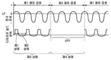
[변형예 1-1∼1-3][Modifications 1-1 to 1-3]
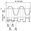
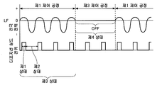
다음으로, 일 실시형태의 변형예 1-1∼1-3에 따른 플라즈마 처리 장치(1)의 제어 방법에 대해 설명한다. 도 9, 도 10a, 도 10b는 일 실시형태의 변형예 1-1∼1-3에 따른 제어 방법을 도시한 타이밍 차트이다. 도 9의 변형예 1-1에서는, DC 펄스의 전압은, 제1 제어 공정에 있어서 제1 상태와 제2 상태를 교대로 1회 이상 반복한다. 제1 제어 공정에서는, LF의 주파수는, 예컨대 0.1 ㎐∼100 ㎐여도 좋다.Next, a control method of the
도 9의 변형예 1-1에서는, LF 전압 대신에 DC 펄스가 배치대(16)에 인가된다. DC 펄스의 전압의 정의 값은, LF 전압의 정의 피크에 일치하고, DC 펄스의 전압의 부의 값 또는 0은, LF 전압의 부의 피크에 일치하며, 디포지션 실드(11)에 인가하는 직류 전압이 제1 상태와 제2 상태가 되도록 DC 펄스의 전압에 동기하여 직류 전압을 교대로 인가한다. 구체적으로는, DC 펄스의 전압이 정인 타이밍에 디포지션 실드(11)의 전위는 제1 상태가 되고, DC 펄스의 전압이 부인 타이밍에 디포지션 실드(11)의 전위가 제2 상태가 되도록 직류 전압을 제어해도 좋다. 이에 의하면, DC 펄스의 전압이 2치화되어 있고, 이에 따라 직류 전압을 2치화하여 제어하기 때문에, 직류 전압의 인가의 제어가 용이해진다. 한편, 직류 전압을 주기적으로 온·오프하는 대신에, 직류 전압을 주기적으로 High·Low가 되도록 제어해도 좋다. In the modified example 1-1 of Fig. 9, a DC pulse is applied to the placing table 16 instead of the LF voltage. The positive value of the voltage of the DC pulse coincides with the positive peak of the LF voltage, and the negative value or 0 of the voltage of the DC pulse coincides with the negative peak of the LF voltage, and the direct current voltage applied to the
도 10a의 변형예 1-2에서는, 직류 전압은, 제1 상태에 있어서 정의 값이고 단계적으로 2개 이상의 전압값을 가지며, 제2 상태에 있어서 0으로 제어된다. 또한, 도 10b의 변형예 1-3에서는, 직류 전압은, 제1 상태에 있어서 정의 값이고 매끄럽게 2개 이상의 전압값을 가지며, 제2 상태에 있어서 매끄럽게 부의 전압값을 갖는다. 변형예 1-2, 1-3에서는, 제1 상태 또는 제2 상태에 있어서의 직류 전압을 복수의 값으로 제어함으로써, 보다 정밀도 좋게 이온 에너지를 제어할 수 있다.In the modified example 1-2 of Fig. 10A, the DC voltage is a positive value in the first state and has two or more voltage values in stages, and is controlled to zero in the second state. In addition, in the modified example 1-3 of Fig. 10B, the direct current voltage is a positive value in the first state, has two or more voltage values smoothly, and has a negative voltage value smoothly in the second state. In the modified examples 1-2 and 1-3, the ion energy can be more accurately controlled by controlling the DC voltage in the first state or the second state to a plurality of values.
상기한 실시형태 및 각 변형예에서는, 전극 전위의 전압의 주기와 동기하여 직류 전압을 인가하는 제어 방법의 일례로서, 바이어스 파워의 전압의 주기와 동기하여 직류 전압을 인가하는 제어 방법에 대해 설명하였다. 그러나, 소스 파워의 전압의 주기와 동기하여 직류 전압을 인가해도 좋다. 바이어스 파워 또는 소스 파워의 전압의 주기와 동기하여 직류 전압 및 소스 파워의 전압 중 적어도 어느 하나를 인가해도 좋다.In the above-described embodiment and each modification, as an example of a control method for applying a DC voltage in synchronization with the period of the voltage of the electrode potential, a control method for applying a DC voltage in synchronization with the period of the voltage of the bias power has been described. . However, a DC voltage may be applied in synchronization with the period of the voltage of the source power. At least one of a DC voltage and a voltage of the source power may be applied in synchronization with the period of the voltage of the bias power or the source power.
이상에서는, 가변 직류 전원(115) 또는 가변 직류 전원(117)으로부터 처리 용기(10)의 디포지션 실드(11)에 인가하는 직류 전압에 대한 제어 방법을 설명하였으나, 이것에 한정되지 않는다. 예컨대, 고주파 전원[제1 고주파 전원(48)]으로부터 처리 용기(10)의 디포지션 실드(11)에 인가하는 고주파 전압에 대해서도 직류 전압에 대한 제어 방법과 동일하게 제어할 수 있다.In the above, the control method for the DC voltage applied from the variable
즉, 본 실시형태에 따른 플라즈마 처리 장치는, 처리 용기와, 처리 용기 내에서 피처리체를 배치하는 전극과, 처리 용기 내에 플라즈마를 공급하는 플라즈마 생성원과, 전극에 바이어스 파워를 공급하는 바이어스 전원과, 처리 용기 내의 플라즈마에 폭로되는 파트와, 바이어스 파워의 전압의 주파수와 동일한 주파수를 갖는 고주파 전압을 파트에 공급하는 고주파 전원과, 전극의 전위의 위상에 대해 미리 정해진 위상차를 발생시키도록 고주파 전압을 인가하는 제1 제어 순서를 포함하는 프로그램을 갖는 기억 매체와, 상기 기억 매체의 프로그램을 실행하는 제어부를 가져도 좋다. 미리 정해진 위상차는, 90°∼270°여도 좋다.That is, the plasma processing apparatus according to the present embodiment includes a processing container, an electrode for placing an object in the processing container, a plasma generation source for supplying plasma in the processing container, and a bias power supply for supplying bias power to the electrode. , A part exposed to the plasma in the processing vessel, a high frequency power supply supplying a high frequency voltage having a frequency equal to the frequency of the voltage of the bias power, and a high frequency voltage to generate a predetermined phase difference with respect to the phase of the potential of the electrode. A storage medium having a program including a first control procedure to be applied, and a control unit for executing the program of the storage medium may be provided. The predetermined phase difference may be 90° to 270°.
또한, 바이어스 전원으로부터 출력되는 고주파 전압용의 제어 신호를 생성하고, 생성된 상기 제어 신호를 위상 시프트 회로에 송신하며, 위상 시프트 회로로부터 상기 에지 링에 고주파 전압을 공급해도 좋다.Further, a control signal for a high-frequency voltage output from a bias power supply may be generated, the generated control signal may be transmitted to a phase shift circuit, and a high-frequency voltage may be supplied to the edge ring from the phase shift circuit.
또한, 예컨대, 직류 전압에 삼각파로 출력되는 전압을 합성하는 등, 직류 전압에 다른 전압을 합성한 전압을 가해도 좋다.Further, a voltage obtained by synthesizing other voltages may be applied to the DC voltage, for example, by synthesizing a voltage output by a triangular wave to the DC voltage.
상기 프로그램은, CD-ROM, DVD 등의 가반성의 컴퓨터 판독 가능한 기억 매체에 수용된 상태로 미리 정해진 위치에 세팅되고, 제어부에 의해 판독되도록 해도 좋다.The program may be set in a predetermined position in a state accommodated in a portable computer-readable storage medium such as a CD-ROM or DVD, and may be read by a control unit.
[변형예 1-4∼1-6][Modifications 1-4 to 1-6]
다음으로, 일 실시형태의 변형예 1-4∼1-6에 따른 플라즈마 처리 장치(1)의 제어 방법에 대해, 도 11 내지 도 13을 참조하여 설명한다. 도 11은 일 실시형태의 변형예 1-4에 따른 제어 방법을 도시한 타이밍 차트이다. 도 12는 일 실시형태의 변형예 1-5에 따른 제어 방법을 도시한 타이밍 차트이다. 도 13은 일 실시형태의 변형예 1-6에 따른 제어 방법을 도시한 타이밍 차트이다.Next, a control method of the
도 11에 도시된 변형예 1-4에서는, 직류 전압은, LF 전압 또는 바이어스 파워의 1주기를 4존으로 나누고, 각 존에 따라 미리 정해진 값의 직류 전압으로 제어되어, 디포지션 실드(11)에 인가된다. 즉, 제1 제어 공정에 있어서 제1 존의 제1 상태와, 제2 존의 제2 상태와, 제3 존의 제3 상태와, 제4 존의 제4 상태를 이 순서로 1회 이상 반복한다. 이에 의해, 디포지션 실드(11)의 전위는, 4개의 상태(고정값)로 제어된다. 변형예 1-4에서는, 인접하는 존에 인가되는 전압은 상이한 값이며 일정한 값이다. 한편, 제1 제어 공정에서는, LF의 주파수는, 예컨대 0.1 ㎐∼100 ㎐여도 좋다.In the modified example 1-4 shown in FIG. 11, the DC voltage is divided into four zones of one period of the LF voltage or bias power, and controlled by a DC voltage of a predetermined value according to each zone, to thereby set the
도 12에 도시된 변형예 1-5에서는, 원하는 파형의 바이어스 파워를 사용한다. 바이어스 파워는, 이러한 바이어스 파워의 파형은, 원하는 파형(바이어스 파형)의 일례이다. 원하는 바이어스 파형은, 도 12에 도시된 바와 같이 임의의 파형이며, 그 1주기를 4존으로 나누고, 각 존에 따라 미리 정해진 값의 직류 전압이 디포지션 실드(11)에 인가된다. 즉, 제1 제어 공정에 있어서 제1 존의 제1 상태와, 제2 존의 제2 상태와, 제3 존의 제3 상태와, 제4 존의 제4 상태를 이 순서로 1회 이상 LF의 주기에 맞춰 반복한다. 이에 의해, 디포지션 실드(11)의 전위는, 4개의 상태(고정값)로 제어된다. 변형예 1-5에서는, 인접하는 존에 인가되는 전압은 상이한 값이며 일정한 값이다.In the modified example 1-5 shown in Fig. 12, bias power of a desired waveform is used. The bias power is an example of a desired waveform (bias waveform). The desired bias waveform is an arbitrary waveform as shown in FIG. 12, and one period is divided into four zones, and a DC voltage of a predetermined value is applied to the
도 13에 도시된 변형예 1-6도, 변형예 1-5와 동일한 바이어스 파형의 1주기를 4존으로 나누고, 각 존에 따라 미리 정해진 값의 직류 전압이 디포지션 실드(11)에 인가된다. 제1 제어 공정에 있어서 제1 존의 제1 상태와, 제2 존의 제2 상태와, 제3 존의 제3 상태와, 제4 존의 제4 상태를 이 순서로 1회 이상 LF의 주기에 맞춰 반복한다. 이에 의해, 디포지션 실드(11)의 전위는, 4개의 상태(가변값을 포함함)로 제어된다. 도 13의 예에서는, 제1 존에서 인가되는 전압은, 시점으로부터 종점까지 전위가 경사지게 변화하는 가변값이다. 제2 존∼제4 존에서 인가되는 전압은, 고정값이다. 제1 존에 나타내는 파형을 테일러드 파형이라고도 한다.In Fig. 13, 1-6 cycles of the same bias waveform as those of Variation 1-6 and Variation 1-5 are divided into four zones, and a DC voltage of a predetermined value is applied to the
이상으로 설명한 바와 같이, 바이어스 파워를 전극에 공급하는 바이어스 전원으로서 LF 전력을 공급하는 제1 고주파 전원(48) 대신에, 원하는 바이어스 파형의 바이어스 파워를 전극에 공급하는 전원을 가져도 좋다. 이 경우, 바이어스 파형의 바이어스 파워의 1주기를 복수의 존으로 분할하여 각 존에 따라, 직류 전압이, 제1 전압값을 갖는 제1 상태와, 제1 전압값과는 상이한 제2 전압값을 갖는 제2 상태와, 제2 전압값과는 상이한 제3 전압값을 갖는 제3 상태와, 제3 전압값과는 상이한 제4 전압값을 갖는 제4 상태를 주기적으로 반복하여, 전극의 전위의 각 주기 내의 부분 기간에 제1 전압값을 인가하고, 제1 상태와 제2 상태가 연속되도록 제2 전압값을 인가하며, 제2 상태와 제3 상태가 연속되도록 제3 전압값을 인가하고, 제3 상태와 제4 상태가 연속되도록 제2 전압값을 인가하는 제1 제어 순서를 포함하는 프로그램을 갖는 기억 매체를 가져도 좋다. 그리고, 제어부(200)는, 그 기억 매체의 프로그램을 실행해도 좋다. 이에 의해, 바이어스 파형의 1주기를 복수의 존으로 나누고, 존마다 고정 또는 가변의 전압을 인가하도록 제어함으로써, 이온의 충돌 에너지를 제어할 수 있다. 바이어스 파형의 1주기를 나누는 존수는 2 이상이면 된다. 이에 의해, 바이어스 파형의 1주기에 2 이상의 상태의 전압을 디포지션 실드(11) 등의 파트에 인가할 수 있다.As described above, instead of the first high
원하는 바이어스 파형은, LF(RF), DC 펄스에 한하지 않는다. 원하는 바이어스 파형은, 도 12 및 도 13에 도시된 테일러드 파형을 포함하는 파형이어도 좋다. 바이어스 파형의 신호는, 발신기[도 3c의 프로세서(100) 참조]에서 생성하고, 생성된 신호를 증폭기로 증폭하여 임의의 파형의 파워를 공급하는 전원에 출력함으로써 생성할 수 있다. 전술한 바이어스 파워는, 원하는 바이어스 파형의 파워의 일례이다. 가변 직류 전원(115)은, 파트에 원하는 바이어스 파형의 전압을 공급하는 전원의 일례이다. 가변 직류 전원(115)을 대신하여 배치될 수 있는 교류 전원으로부터 파트에 원하는 바이어스 파형의 전압을 공급해도 좋다. 또한, 제1 고주파 전원(48)도 마찬가지로, 전극에 원하는 바이어스 파형의 파워를 공급하는 바이어스 전원의 일례이다. 배치대(16)에 제2 고주파 전원(90)과는 다른 RF 파워를 인가하는 RF 전원을 별도로 설치해도 좋다. 이 경우, 제2 고주파 전원(90) 및 RF 전원은, 원하는 바이어스 파형의 파워의 전압의 주파수와 동일 또는 상이한 주파수를 갖는 고주파 전압을 디포지션 실드(11) 등의 파트에 공급하는 전원의 일례이다.The desired bias waveform is not limited to LF (RF) and DC pulses. The desired bias waveform may be a waveform including the tailored waveforms shown in FIGS. 12 and 13. The signal of the bias waveform can be generated by generating the signal from the transmitter (see
디포지션 실드(11)에 인가하는 전압은, 직류 전압을 온·오프할 뿐만이 아니라, 고주파 RF의 파워를 변경해도 좋고, 도 13의 디포지션 실드(11)의 전위에 나타내는 바와 같이 임의로 형성된 바이어스 파형을 인가해도 좋다. 직류 전압 및 고주파 RF의 파워를 제어하고, 또한 고주파 RF의 주파수를 변경해도 좋다. 디포지션 실드(11) 등의 파트에 인가하는 전압은, 프로세스 레시피에 대응하여 제어부(200)에 의해 제어해도 좋다.The voltage applied to the
[변형예 2-1∼2-4][Modifications 2-1 to 2-4]
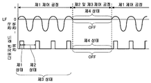
다음으로, 일 실시형태의 변형예 2-1∼2-4에 따른 플라즈마 처리 장치(1)의 제어 방법에 대해 설명한다. 변형예 2-1∼2-4에서는, 바이어스 파워와 직류 전압 중 어느 하나 또는 양방을 간헐적으로 정지하는 제어를 행한다. 도 14a 내지 도 14d는 일 실시형태의 변형예 2-1∼2-4에 따른 제어 방법을 도시한 타이밍 차트이다.Next, a control method of the
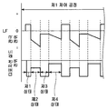
도 14a의 변형예 2-1에서는, 제1 제어 공정에 더하여, 직류 전압을, LF 전압에 의해 일례를 나타내는 주기적으로 변동하는 파라미터의 주기와 독립된 주기로 간헐적으로 정지하는 제2 제어 공정을 포함한다. 제1 제어 공정과 제2 제어 공정은 반복해서 실행된다.In the modified example 2-1 of Fig. 14A, in addition to the first control process, the second control process includes intermittently stopping the DC voltage in a cycle independent of the period of the periodically varying parameter representing an example by the LF voltage. The first control process and the second control process are repeatedly executed.
변형예 2-1에서는, LF 전압은, 제1 제어 공정 및 제2 제어 공정에 있어서 동일한 주기로 인가된다. 한편, DC 전압은, 제1 제어 공정에 있어서 제1 상태와 제2 상태를 교대로 1회 이상 반복하고, 제2 제어 공정에 있어서 제1 제어 공정 사이에서 간헐적으로 정지된다.In modification 2-1, the LF voltage is applied in the same cycle in the first control process and the second control process. On the other hand, the DC voltage repeats the first state and the second state one or more times alternately in the first control process, and is intermittently stopped between the first control process in the second control process.
제1 제어 공정 및 제2 제어 공정에서는, LF의 주파수는, 예컨대 0.1 ㎐∼100 ㎑여도 좋다. 도 14a의 변형예 2-1 내지 도 14d의 변형예 2-4에서는, 처리 용기의 디포지션 실드(11)의 전위가 제1 상태가 되도록, 전극 전위를 일례로 하는 주기적으로 변동하는 파라미터가 정의 값을 포함하는 부분 기간에 직류 전압을 인가하고, 제2 상태를 제1 상태와 연속해서 인가한다. 직류 전압의 경우, 정의 값이며, 제1 상태의 제1 전압값이 제2 상태의 제2 전압값보다 높다.In the first control step and the second control step, the frequency of LF may be, for example, 0.1 kHz to 100 kHz. In the modified examples 2-1 to 14D of Fig. 14A to the modified example 2-4 of Fig. 14D, a parameter that periodically fluctuates using the electrode potential as an example is defined so that the potential of the
도 14a의 변형예 2-1 내지 도 14d의 변형예 2-4에서는, DC 전압의 제1 상태가 정의 전압값을 갖고, 제2 상태가 0이다. 한편, 직류 전압의 Duty비[=제4 상태/(제3 상태+제4 상태)]는, 1%∼99%의 범위 내이면 된다.In the modified examples 2-1 to 14D of Fig. 14A, the first state of the DC voltage has a positive voltage value, and the second state is 0. On the other hand, the duty ratio [= fourth state/(third state+fourth state)] of the DC voltage may be within a range of 1% to 99%.
미리 정해진 고주파 전압(이하, 「RF 전압」이라고도 함)을 처리 용기의 디포지션 실드(11)에 공급해도 좋다. 이 경우, 제2 고주파 전원(90)으로부터, RF 전압을 처리 용기의 디포지션 실드(11)에 공급해도 좋고, 배치대(16)에 RF 전압을 인가하는 RF 전원을 별도로 설치해도 좋다. RF 전압은, 제1 상태의 제1 전압값이 제2 상태의 제2 전압값보다 높다.A predetermined high-frequency voltage (hereinafter also referred to as "RF voltage") may be supplied to the
도 14a의 변형예 2-1에 있어서, 제1 제어 공정에 있어서의 LF 전압이 정인 타이밍에서 동기한 DC 전압이 제1 상태를 취하고, 0의 제2 상태와 반복되는 것이, 제3 상태의 일례이다. 제2 제어 공정에 있어서의 LF 전압의 주기와 독립된 DC 전압의 상태는, 제3 상태와는 상이한 제4 상태의 일례이다.In the modified example 2-1 of Fig. 14A, an example of the third state is that the DC voltage synchronized at the timing at which the LF voltage in the first control process is positive takes the first state and repeats with the second state of zero. to be. The state of the DC voltage independent of the period of the LF voltage in the second control process is an example of a fourth state different from the third state.
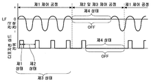
도 14b의 변형예 2-2에 따른 제어 방법은, 변형예 2-1과 동일한 제1 제어 공정에 더하여, 바이어스 파워를 DC 전압의 주기와는 독립된 주기로 간헐적으로 정지하는 제3 제어 공정을 포함한다. 제3 제어 공정에 있어서의 바이어스 파워의 상태는, 제4 상태의 일례이다.The control method according to Modification 2-2 of FIG. 14B includes, in addition to the same first control process as Variation 2-1, a third control process for intermittently stopping the bias power at a period independent of the period of the DC voltage. . The state of the bias power in the third control process is an example of the fourth state.
변형예 2-2에서는, 제1 제어 공정과 제3 제어 공정이 반복해서 실행된다. 변형예 2-2에서는, 제3 제어 공정에 있어서의 DC 전압은, 제1 제어 공정과 동일한 주기로 제1 상태와 제2 상태가 반복된다.In the modification 2-2, the 1st control process and the 3rd control process are performed repeatedly. In the modification 2-2, the DC voltage in the third control process is repeated in the first state and the second state in the same cycle as the first control process.
한편, 제1 제어 공정에 있어서 LF의 주파수는, 예컨대 0.1 ㎐∼100 ㎐여도 좋고, LF 전압의 Duty비[=제4 상태/(제3 상태+제4 상태)]는, 1%∼90%의 범위 내이면 된다.On the other hand, in the first control step, the frequency of LF may be, for example, 0.1 kHz to 100 kHz, and the duty ratio of the LF voltage [=4th state/(3rd state+4th state)] is 1% to 90%. It should just be within the range of.
도 14c의 변형예 2-3에 따른 제어 방법은, 변형예 2-1과 동일한 제1 제어 공정에 더하여, 변형예 2-1의 제2 제어 공정의 DC의 제어와 변형예 2-2의 제3 제어 공정의 LF의 제어가 행해진다. 즉, 변형예 2-3에 있어서의 DC 전압 및 바이어스 파워의 양방을 간헐적으로 정지한 상태는, 제4 상태의 일례이다.The control method according to modified example 2-3 of FIG. 14C is a control of DC of the second control process of modified example 2-1 and the second control process of modified example 2-2, in addition to the same first control process as of modified example 2-1. 3 LF control of the control process is performed. That is, the state in which both the DC voltage and the bias power in the modified examples 2-3 are intermittently stopped is an example of the fourth state.
바이어스 파워를 간헐적으로 정지하는 주기와 DC 전압을 간헐적으로 정지하는 주기는 동기시켜도 좋다. 이 경우, DC 및 바이어스 파워를 간헐적으로 정지하는 주기는, 도 14c에 도시된 바와 같이 일치해도 좋고, 도 14d에 도시된 바와 같이, DC가 바이어스 파워보다 뒤로 어긋나 있어도 좋으며, DC가 바이어스 파워보다 앞으로 어긋나 있어도 좋다.The period for stopping the bias power intermittently and the period for stopping the DC voltage intermittently may be synchronized. In this case, the periods for intermittently stopping the DC and bias powers may coincide as shown in Fig. 14C, or as shown in Fig. 14D, the DCs may deviate from the bias powers backward, and the DCs may be forwarded from the bias powers. It may be shifted.
한편, 도 14a 내지 도 14d에서는, 제3 상태에 있어서, 바이어스 파워가 정인 일부의 타이밍에, DC 전압을 온하고 있으나, 이것에 한정되지 않는다. 또한, DC 전압을 주기적으로 온·오프하는 대신에, DC 전압을 정의 값이며 주기적으로 절대값이 High·Low가 되도록 제어해도 좋다.On the other hand, in Figs. 14A to 14D, in the third state, the DC voltage is turned on at a part of the timing at which the bias power is positive, but is not limited to this. Further, instead of periodically turning the DC voltage on and off, the DC voltage may be controlled to be a positive value and the absolute value to be periodically high and low.
[변형예 3][Modification 3]
다음으로, 일 실시형태의 변형예 3에 따른 제어 방법에 대해, 도 15를 참조하여 설명한다. 도 11은 일 실시형태의 변형예 3에 따른 제어 방법을 도시한 타이밍 차트이다.Next, a control method according to Modification Example 3 of one embodiment will be described with reference to FIG. 15. 11 is a timing chart showing a control method according to Modification Example 3 of an embodiment.
예컨대, 변형예 3에 따른 제어 방법에서는, 도 15에 도시된 바와 같이 DC 펄스가 배치대(16)에 인가된다. DC 펄스의 정의 값은, LF 전압의 정의 피크에 일치하고, DC 펄스의 부의 값은, LF 전압의 부의 피크에 일치한다.For example, in the control method according to Modification 3, a DC pulse is applied to the placing table 16 as shown in FIG. The positive value of the DC pulse coincides with the positive peak of the LF voltage, and the negative value of the DC pulse coincides with the negative peak of the LF voltage.
이 경우, 변형예 3에 따른 제어 방법에서는, 정의 직류 전압 또는 고주파 전압은 제1 상태와 제2 상태를 주기적으로 반복하여, 제1 상태를, DC 펄스의 각 주기 내의 부분 기간에 인가하고, 제2 상태를 제1 상태와 연속해서 인가한다. 이에 의해서도, 웨이퍼(W)의 에지부의 홀의 타원 형상이나 틸팅의 발생을 방지할 수 있다.In this case, in the control method according to Variation 3, the positive DC voltage or the high frequency voltage periodically repeats the first state and the second state, and applies the first state to a partial period within each cycle of the DC pulse. 2 states are continuously applied to the first state. Also by this, it is possible to prevent the elliptical shape of the hole in the edge portion of the wafer W and the occurrence of tilting.
예컨대, DC 펄스가 0 또는 정인 동안의 일부 또는 전부에 있어서 직류 전압은, 제1 상태의 제1 전압값으로 제어되고, DC 펄스가 부인 동안의 일부 또는 전부에 있어서 제2 상태의 제2 전압값은, 제1 상태의 제1 전압값보다 낮아지도록 제어해도 좋다. 이에 의하면, DC 펄스가 2치화되어 있고, 이에 따라 DC 전압을 2치화하여 제어하기 때문에, 제어가 용이해진다.For example, the DC voltage in part or all while the DC pulse is 0 or positive is controlled by the first voltage value in the first state, and the second voltage value in the second state in part or all while the DC pulse is negated. May be controlled to be lower than the first voltage value in the first state. According to this, since the DC pulse is binarized and, accordingly, the DC voltage is binarized and controlled, control becomes easy.
[변형예 4-1, 4-2][Modifications 4-1, 4-2]
도 16a는 일 실시형태의 변형예 4-1에 따른 제어 방법을 도시한 타이밍 차트이다. 도 16b는 일 실시형태의 변형예 4-2에 따른 제어 방법을 도시한 타이밍 차트이다. 예컨대, 도 16a 및 도 16b에 도시된 변형예 4-1, 4-2에 따른 제어 방법에서는, 처리 용기의 디포지션 실드(11)의 전위가 제1 상태가 되도록, 전극 전위를 일례로 하는 주기적으로 변동하는 파라미터가 정의 값을 포함하는 부분 기간에 고주파 전압을 인가하고, 제2 상태를 제1 상태와 연속해서 인가한다. 도 16a에 도시된 변형예 4-1에서는, DC 전압의 제1 상태가, 정의 값이고 단계적으로 2개 이상의 제1 전압값을 갖는다. 이 경우에도 정의 전압은, 제1 상태의 제1 전압값이 제2 상태의 제2 전압값보다 높다.16A is a timing chart showing a control method according to Modification Example 4-1 of an embodiment. 16B is a timing chart showing a control method according to Modification Example 4-2 of an embodiment. For example, in the control method according to the modified examples 4-1 and 4-2 shown in Figs. 16A and 16B, the periodicity of the electrode potential as an example is such that the potential of the
고주파 전압을 인가하는 경우에는, 제1 상태의 제1 전압값이 제2 상태의 제2 전압값의 절대값보다 크다. 고주파 전압은, 제2 고주파 전원(90)으로부터 처리 용기의 디포지션 실드(11)에 공급해도 좋고, 고주파 전압을 인가하는 RF 전원을 별도로 설치해도 좋다.When a high frequency voltage is applied, the first voltage value in the first state is greater than the absolute value of the second voltage value in the second state. The high frequency voltage may be supplied from the second high
도 16b에 도시된 변형예 4-2에서는, 고주파 전압의 제1 상태가, 매끄럽게 2개 이상의 제1 전압값을 갖는다. 도 16a 및 도 16b의 어느 경우에도, 제1 상태와 제2 상태는 주기적으로 반복된다.In the modification 4-2 shown in Fig. 16B, the first state of the high-frequency voltage has two or more first voltage values smoothly. In either case of FIGS. 16A and 16B, the first state and the second state are periodically repeated.
예컨대, 도 16a에 도시된 변형예 4-1에서는, 직류 전압의 제1 상태가, 정의 값이고 단계적으로 2개 이상의 제1 전압값을 갖는다. 이 경우에도, 제1 상태의 제1 전압값이 제2 상태의 제2 전압값보다 높다.For example, in the modified example 4-1 shown in Fig. 16A, the first state of the DC voltage is a positive value and has two or more first voltage values in steps. Also in this case, the first voltage value in the first state is higher than the second voltage value in the second state.
(그 외)(etc)
제어부(200)의 제어에 대해 부기한다.The control of the
(부기 1)(Annex 1)
제어부(200)는, 상기 제1 상태의 기간에 소스 파워를 공급해도 좋다.The
(부기 2)(Bookkeeping 2)
제1 상태의 기간은, 하부 전극 또는 상부 전극이 정의 피크가 되는 타이밍을 포함해도 좋다.The period in the first state may include a timing at which the lower electrode or the upper electrode becomes a positive peak.
(부기 3)(Annex 3)
제어부(200)는, 상기 전극 전위가 정의 타이밍인 시간에 소스 파워 및 직류 전압 중 적어도 어느 하나를 공급해도 좋다.The
(부기 4)(Annex 4)
제어부(200)는, 상기 전극 전위가 정인 타이밍으로부터 미리 정해진 시간 시프트시킨 시간에 소스 파워 및 직류 전압 중 적어도 어느 하나를 공급해도 좋다.The
(부기 5)(Bookkeeping 5)
제어부(200)는, 상기 전극 전위가 정인 타이밍으로부터 미리 정해진 시간의 마진을 부가한 시간에 소스 파워 및 직류 전압 중 적어도 어느 하나를 공급해도 좋다.The
이상, 제어 방법 및 플라즈마 처리 장치를 상기 실시형태에 의해 설명하였으나, 본 개시에 따른 제어 방법 및 플라즈마 처리 장치는 상기 실시형태에 한정되는 것은 아니며, 본 개시의 범위 내에서 여러 가지 변형 및 개량이 가능하다. 상기 복수의 실시형태에 기재된 사항은, 모순되지 않는 범위에서 조합할 수 있다. 또한, 일 실시형태 및 복수의 변형예는, 모순되지 않는 범위에서 조합할 수 있다.In the above, the control method and the plasma processing apparatus have been described by the above embodiments, but the control method and the plasma processing apparatus according to the present disclosure are not limited to the above embodiments, and various modifications and improvements are possible within the scope of the present disclosure. Do. The items described in the plurality of embodiments can be combined within a range that does not contradict. In addition, one embodiment and a plurality of modified examples can be combined within a range that does not contradict.
본 개시에 따른 플라즈마 처리 장치는, CCP(Capacitively Coupled Plasma), ICP(Inductively Coupled Plasma), RLSA(Radial Line Slot Antenna), ECR(Electron Cyclotron Resonance Plasma), HWP(Helicon Wave Plasma)의 어느 타입에도 적용 가능하다.The plasma processing apparatus according to the present disclosure is applied to any type of capacitively coupled plasma (CCP), inductively coupled plasma (ICP), radial line slot antenna (RLSA), electron cyclotron resonance plasma (ECR), or Helical wave plasma (HWP) It is possible.
상기 바이어스 파워보다 높은 주파수를 갖는 소스 파워를 플라즈마 처리 공간에 공급하는 공정은, 플라즈마를 생성하기 위한 플라즈마 생성원이, 마이크로파원, 고주파 전원 등의 소스 파워를 플라즈마 처리 공간에 공급함으로써 실행되어도 좋다.The step of supplying a source power having a frequency higher than the bias power to the plasma processing space may be performed by supplying a source power such as a microwave source or a high-frequency power source to the plasma processing space.
본 명세서에서는, 피처리체의 일례로서 반도체 웨이퍼(W)를 들어 설명하였다. 그러나, 피처리체는, 이것에 한하지 않고, LCD(Liquid Crystal Display), FPD(Flat Panel Display)에 이용되는 각종 기판, CD 기판, 프린트 기판 등이어도 좋다.In this specification, the semiconductor wafer W is described as an example of the object to be processed. However, the object to be processed is not limited to this, and various substrates, CD substrates, and printed substrates used for LCD (Liquid Crystal Display) and FPD (Flat Panel Display) may be used.
Claims (18)
상기 처리 용기 내에서 피처리체를 배치하는 전극과,
상기 처리 용기 내에 플라즈마를 공급하는 플라즈마 생성원과,
상기 전극에 원하는 파형의 바이어스 파워를 공급하는 바이어스 전원과,
상기 처리 용기 내의 플라즈마에 폭로(暴露)되는 파트와,
상기 파트에 원하는 파형의 전압을 공급하는 전원과,
상기 전압이, 제1 전압값을 갖는 제1 상태와, 상기 제1 전압값보다 높은 제2 전압값을 갖는 제2 상태를 주기적으로 반복하여, 상기 전극의 전위의 각 주기 내의 부분 기간에 상기 제1 전압값을 인가하고, 상기 제1 상태와 상기 제2 상태가 연속되도록 상기 제2 전압값을 인가하는 제1 제어 순서를 포함하는 프로그램을 갖는 기억 매체와,
상기 기억 매체의 프로그램을 실행하는 제어부
를 갖는, 플라즈마 처리 장치.A processing container,
An electrode for disposing the object to be processed in the processing container,
A plasma generation source that supplies plasma into the processing vessel,
A bias power supply for supplying a bias power having a desired waveform to the electrode;
A part exposed to plasma in the processing container,
Power supply for supplying the voltage of the desired waveform to the part,
The voltage is periodically repeated in a first state having a first voltage value and a second state having a second voltage value higher than the first voltage value, so that the first time is a partial period within each period of the potential of the electrode. A storage medium having a program including a first control procedure for applying one voltage value and applying the second voltage value so that the first state and the second state are continuous;
A control unit for executing the program of the storage medium
Having a plasma processing apparatus.
상기 주기적으로 변동하는 파라미터는, 전압, 전류, 전자계, 발생한 플라즈마의 발광의 변화 또는 피처리체 상의 플라즈마의 시스 두께의 변화인, 플라즈마 처리 장치.The method according to claim 1, wherein the potential of the electrode is determined by a periodically synchronous parameter measured in a transmission path of the bias power, or a signal synchronized with a period of a high frequency or pulse wave of the bias power,
The periodically fluctuating parameter is a change in voltage, current, electromagnetic field, light emission of the generated plasma, or a change in the sheath thickness of the plasma on the object to be processed.
상기 제어부는, 상기 기억 매체의 프로그램을 실행하는, 플라즈마 처리 장치.9. The storage medium according to any one of claims 1 to 8, wherein the storage medium periodically repeats the voltage, the first state, the second state, and two or more states having two or more voltage values. , The first voltage value is applied to a partial period within each period of the potential of the electrode, and the second voltage value, the two or more voltage values such that the first state, the second state, and the two or more states are continuous. It includes the above program to authorize in order,
The control unit executes a program of the storage medium, a plasma processing apparatus.
상기 제어부는, 상기 기억 매체의 프로그램을 실행하는, 플라즈마 처리 장치.The memory medium according to any one of claims 1 to 9, wherein the storage medium has a program including a second control sequence in which the voltage intermittently stops at a period independent of the period of the first control sequence,
The control unit executes a program of the storage medium, a plasma processing apparatus.
상기 처리 용기 내에서 피처리체를 배치하는 전극과,
상기 처리 용기 내에 플라즈마를 공급하는 플라즈마 생성원과,
상기 전극에 원하는 파형의 바이어스 파워를 공급하는 바이어스 전원과,
상기 처리 용기 내의 플라즈마에 폭로되는 파트와,
상기 원하는 파형의 바이어스 파워의 전압의 주파수와 동일 또는 상기 주파수보다 높은 주파수를 갖는 고주파 전압을 상기 파트에 공급하는 고주파 전원과,
상기 전극의 전위의 위상에 대해 미리 정해진 위상차를 발생시키도록 상기 고주파 전압을 인가하는 제1 제어 순서를 포함하는 프로그램을 갖는 기억 매체와,
상기 기억 매체의 프로그램을 실행하는 제어부
를 갖는, 플라즈마 처리 장치.A processing container,
An electrode for disposing the object to be processed in the processing container,
A plasma generation source that supplies plasma into the processing vessel,
A bias power supply for supplying a bias power having a desired waveform to the electrode;
A part exposed to plasma in the processing container,
A high frequency power supply for supplying a high frequency voltage to the part having a frequency equal to or higher than the frequency of the voltage of the bias power of the desired waveform;
A storage medium having a program including a first control procedure for applying the high frequency voltage to generate a predetermined phase difference with respect to the phase of the potential of the electrode;
A control unit for executing the program of the storage medium
Having a plasma processing apparatus.
상기 처리 용기 내에서 피처리체를 배치하는 전극과,
상기 처리 용기 내에 플라즈마를 공급하는 플라즈마 생성원과,
상기 전극에 원하는 파형의 바이어스 파워를 공급하는 바이어스 전원과,
상기 처리 용기 내의 플라즈마에 폭로되는 파트와,
상기 파트에 원하는 파형의 전압을 공급하는 전원
을 갖는 플라즈마 처리 장치의 제어 방법에 있어서,
상기 전압이, 제1 전압값을 갖는 제1 상태와, 상기 제1 전압값보다 높은 제2 전압값을 갖는 제2 상태를 주기적으로 반복하는 공정과,
상기 전극의 전위의 각 주기 내의 부분 기간에 상기 제1 전압값을 인가하고, 상기 제1 상태와 상기 제2 상태가 연속되도록 상기 제2 전압값을 인가하는 공정
을 갖는, 플라즈마 처리 장치의 제어 방법.A processing container,
An electrode for disposing the object to be processed in the processing container,
A plasma generation source that supplies plasma into the processing vessel,
A bias power supply for supplying a bias power having a desired waveform to the electrode;
A part exposed to plasma in the processing container,
Power supply that supplies the desired waveform voltage to the part
In the control method of the plasma processing apparatus having a,
A step of periodically repeating a first state in which the voltage has a first voltage value and a second state in which a second voltage value is higher than the first voltage value,
A step of applying the first voltage value to a partial period within each period of the potential of the electrode, and applying the second voltage value such that the first state and the second state are continuous;
It has a, the control method of the plasma processing apparatus.
상기 전원과 상기 위상 시프트 회로 중 적어도 어느 하나로부터 상기 파트에 전압을 공급하는, 플라즈마 처리 장치의 제어 방법.15. The method of claim 14, Creating a synchronization signal synchronized with the potential of the electrode, generating a control signal for the power supply output from the synchronization signal, the generated control signal at least one of the power supply and the phase shift circuit Send to one,
A control method of a plasma processing apparatus that supplies a voltage to the part from at least one of the power supply and the phase shift circuit.
상기 처리 용기 내에서 피처리체를 배치하는 전극과,
상기 처리 용기 내에 플라즈마를 공급하는 플라즈마 생성원과,
상기 전극에 원하는 파형의 바이어스 파워를 공급하는 바이어스 전원과,
상기 처리 용기 내의 플라즈마에 폭로되는 파트와,
상기 원하는 파형의 바이어스 파워의 전압의 주파수와 동일한 주파수를 갖는 고주파 전압을 상기 파트에 공급하는 전원
을 갖는 플라즈마 처리 장치의 제어 방법에 있어서,
상기 전극의 전위의 위상에 대해 미리 정해진 위상차를 발생시키도록 상기 고주파 전압을 인가하는, 플라즈마 처리 장치의 제어 방법.A processing container,
An electrode for disposing the object to be processed in the processing container,
A plasma generation source that supplies plasma into the processing vessel,
A bias power supply for supplying a bias power having a desired waveform to the electrode;
A part exposed to plasma in the processing container,
A power supply supplying a high frequency voltage having the same frequency as the voltage of the bias power of the desired waveform to the part
In the control method of the plasma processing apparatus having a,
And applying the high frequency voltage to generate a predetermined phase difference with respect to the phase of the potential of the electrode.
상기 위상 시프트 회로로부터 상기 파트에 고주파 전압을 공급하는, 플라즈마 처리 장치의 제어 방법. 18. The method of claim 17, Generating a control signal for a high-frequency voltage output from the bias power supply, and transmits the generated control signal to a phase shift circuit,
The control method of the plasma processing apparatus which supplies a high frequency voltage to the said part from the said phase shift circuit.
Applications Claiming Priority (4)
| Application Number | Priority Date | Filing Date | Title |
|---|---|---|---|
| JPJP-P-2018-248260 | 2018-12-28 | ||
| JP2018248260 | 2018-12-28 | ||
| JP2019224853A JP7345382B2 (en) | 2018-12-28 | 2019-12-12 | Plasma processing equipment and control method |
| JPJP-P-2019-224853 | 2019-12-12 |
Publications (2)
| Publication Number | Publication Date |
|---|---|
| KR20200083330A true KR20200083330A (en) | 2020-07-08 |
| KR102919563B1 KR102919563B1 (en) | 2026-01-28 |
Family
ID=71570125
Family Applications (1)
| Application Number | Title | Priority Date | Filing Date |
|---|---|---|---|
| KR1020190176574A Active KR102919563B1 (en) | 2018-12-28 | 2019-12-27 | Plasma processing apparatus and control method |
Country Status (4)
| Country | Link |
|---|---|
| US (2) | US11201034B2 (en) |
| JP (1) | JP7345382B2 (en) |
| KR (1) | KR102919563B1 (en) |
| TW (1) | TWI901575B (en) |
Cited By (3)
| Publication number | Priority date | Publication date | Assignee | Title |
|---|---|---|---|---|
| KR20220105541A (en) | 2021-01-20 | 2022-07-27 | 박훈 | Horizontal tyhpe album |
| KR20230056228A (en) * | 2021-10-20 | 2023-04-27 | (주)아이씨디 | Capacitively Coupled Plasma Substrate Processing Apparatus |
| US12249491B2 (en) | 2020-08-07 | 2025-03-11 | Semes Co., Ltd. | Substrate treating apparatus and substrate support unit |
Families Citing this family (13)
| Publication number | Priority date | Publication date | Assignee | Title |
|---|---|---|---|---|
| JP7306886B2 (en) * | 2018-07-30 | 2023-07-11 | 東京エレクトロン株式会社 | Control method and plasma processing apparatus |
| JP7345382B2 (en) * | 2018-12-28 | 2023-09-15 | 東京エレクトロン株式会社 | Plasma processing equipment and control method |
| US11361947B2 (en) * | 2019-01-09 | 2022-06-14 | Tokyo Electron Limited | Apparatus for plasma processing and method of etching |
| JP7278896B2 (en) * | 2019-07-16 | 2023-05-22 | 東京エレクトロン株式会社 | Plasma processing method and plasma processing apparatus |
| CN117293008A (en) | 2019-08-05 | 2023-12-26 | 株式会社日立高新技术 | Plasma treatment equipment |
| JP7597464B2 (en) | 2021-02-10 | 2024-12-10 | 東京エレクトロン株式会社 | Plasma Processing Equipment |
| JP7572126B2 (en) | 2021-04-21 | 2024-10-23 | 東京エレクトロン株式会社 | Electrode for plasma processing apparatus and plasma processing apparatus |
| US12525433B2 (en) | 2021-06-09 | 2026-01-13 | Applied Materials, Inc. | Method and apparatus to reduce feature charging in plasma processing chamber |
| KR102936883B1 (en) * | 2021-08-23 | 2026-03-11 | 주식회사 히타치하이테크 | Plasma treatment device and plasma treatment method |
| TW202331780A (en) * | 2021-09-15 | 2023-08-01 | 日商東京威力科創股份有限公司 | Plasma processing apparatus and plasma processing method |
| JP7607539B2 (en) * | 2021-09-24 | 2024-12-27 | 東京エレクトロン株式会社 | Plasma processing apparatus and processing method |
| US11898236B2 (en) * | 2021-10-20 | 2024-02-13 | Applied Materials, Inc. | Methods and apparatus for processing a substrate |
| JP2024042803A (en) * | 2022-09-16 | 2024-03-29 | キオクシア株式会社 | Plasma processing apparatus, plasma processing method, and semiconductor device manufacturing method |
Citations (1)
| Publication number | Priority date | Publication date | Assignee | Title |
|---|---|---|---|---|
| JP2006286813A (en) | 2005-03-31 | 2006-10-19 | Tokyo Electron Ltd | Plasma processing apparatus and plasma processing method |
Family Cites Families (49)
| Publication number | Priority date | Publication date | Assignee | Title |
|---|---|---|---|---|
| US20050041355A1 (en) * | 1999-01-06 | 2005-02-24 | Page J. Dennis | Monitoring and response system |
| JP3585217B2 (en) * | 2000-07-03 | 2004-11-04 | 東京エレクトロン株式会社 | Substrate processing equipment |
| AUPS057102A0 (en) * | 2002-02-15 | 2002-03-07 | Vri Biomedical Ltd | Compositions and methods for treatment of skin disorders |
| JP4753276B2 (en) * | 2002-11-26 | 2011-08-24 | 東京エレクトロン株式会社 | Plasma processing method and plasma processing apparatus |
| JP4482308B2 (en) * | 2002-11-26 | 2010-06-16 | 東京エレクトロン株式会社 | Plasma processing apparatus and plasma processing method |
| JP4584565B2 (en) * | 2002-11-26 | 2010-11-24 | 東京エレクトロン株式会社 | Plasma processing apparatus and plasma processing method |
| US7215751B2 (en) * | 2004-01-22 | 2007-05-08 | International Business Machines Corporation | System and method for processing caller information across heterogeneous networks |
| JP4523352B2 (en) * | 2004-07-20 | 2010-08-11 | 株式会社日立ハイテクノロジーズ | Plasma processing equipment |
| US20060042754A1 (en) * | 2004-07-30 | 2006-03-02 | Tokyo Electron Limited | Plasma etching apparatus |
| JP5192209B2 (en) * | 2006-10-06 | 2013-05-08 | 東京エレクトロン株式会社 | Plasma etching apparatus, plasma etching method, and computer-readable storage medium |
| US7758764B2 (en) * | 2007-06-28 | 2010-07-20 | Lam Research Corporation | Methods and apparatus for substrate processing |
| JP5432629B2 (en) * | 2009-08-07 | 2014-03-05 | 東京エレクトロン株式会社 | Baffle plate and plasma processing apparatus |
| JP5571996B2 (en) * | 2010-03-31 | 2014-08-13 | 東京エレクトロン株式会社 | Plasma processing method and plasma processing apparatus |
| JP2012104382A (en) * | 2010-11-10 | 2012-05-31 | Tokyo Electron Ltd | Plasma treatment apparatus, plasma treatment method, and plasma treatment bias voltage determination method |
| JP5893864B2 (en) * | 2011-08-02 | 2016-03-23 | 東京エレクトロン株式会社 | Plasma etching method |
| US20130084707A1 (en) * | 2011-09-30 | 2013-04-04 | Tokyo Electron Limited | Dry cleaning method for recovering etch process condition |
| US9922802B2 (en) * | 2012-02-20 | 2018-03-20 | Tokyo Electron Limited | Power supply system, plasma etching apparatus, and plasma etching method |
| JP2013229373A (en) * | 2012-04-24 | 2013-11-07 | Tokyo Electron Ltd | Substrate processing apparatus and maintenance method of the same |
| JP6068849B2 (en) * | 2012-07-17 | 2017-01-25 | 東京エレクトロン株式会社 | Upper electrode and plasma processing apparatus |
| JP6207880B2 (en) * | 2012-09-26 | 2017-10-04 | 東芝メモリ株式会社 | Plasma processing apparatus and plasma processing method |
| US9593421B2 (en) * | 2013-11-06 | 2017-03-14 | Applied Materials, Inc. | Particle generation suppressor by DC bias modulation |
| JP2015095551A (en) * | 2013-11-12 | 2015-05-18 | 東京エレクトロン株式会社 | Shower head assembly and plasma processing apparatus |
| JP6173889B2 (en) * | 2013-11-28 | 2017-08-02 | ソニーセミコンダクタソリューションズ株式会社 | Simulation method, simulation program, machining control system, simulator, process design method and mask design method |
| JP2015115564A (en) * | 2013-12-16 | 2015-06-22 | 株式会社日立ハイテクノロジーズ | Plasma processing apparatus and plasma processing method |
| JP6169040B2 (en) * | 2014-05-12 | 2017-07-26 | 東京エレクトロン株式会社 | Upper electrode structure of plasma processing apparatus, plasma processing apparatus, and method of operating plasma processing apparatus |
| KR101745686B1 (en) * | 2014-07-10 | 2017-06-12 | 도쿄엘렉트론가부시키가이샤 | Methods for high precision etching of substrates |
| KR20160009760A (en) * | 2014-07-16 | 2016-01-27 | 피에스케이 주식회사 | Plasma generating device, plasma characteristic controlling method, and substrate treating apparatus using the same |
| US9779919B2 (en) * | 2015-01-09 | 2017-10-03 | Hitachi High-Technologies Corporation | Plasma processing apparatus and plasma processing method |
| JP6449091B2 (en) * | 2015-04-20 | 2019-01-09 | 東京エレクトロン株式会社 | Slip ring, support mechanism and plasma processing apparatus |
| JP6462477B2 (en) * | 2015-04-27 | 2019-01-30 | 東京エレクトロン株式会社 | Method for processing an object |
| CN108140550B (en) * | 2015-10-08 | 2022-10-14 | 应用材料公司 | Showerhead with reduced backside plasma ignition |
| US9779955B2 (en) * | 2016-02-25 | 2017-10-03 | Lam Research Corporation | Ion beam etching utilizing cryogenic wafer temperatures |
| KR102513443B1 (en) * | 2016-03-15 | 2023-03-24 | 삼성전자주식회사 | electrostatic chuck and substrate processing apparatus including the same |
| US20170278730A1 (en) * | 2016-03-28 | 2017-09-28 | Hitachi High-Technologies Corporation | Plasma processing apparatus and plasma processing method |
| JP2018022830A (en) * | 2016-08-05 | 2018-02-08 | 東京エレクトロン株式会社 | Method for processing an object |
| CN108206143B (en) * | 2016-12-16 | 2020-09-25 | 中微半导体设备(上海)股份有限公司 | A plasma processor, etching uniformity adjustment system and method |
| KR20180134182A (en) * | 2017-06-08 | 2018-12-18 | 삼성전자주식회사 | plasma processing apparatus |
| KR102435263B1 (en) * | 2017-07-25 | 2022-08-23 | 삼성전자주식회사 | Plasma processing apparatus and method, and method of manufacturing semiconductor device using the same |
| US10763083B2 (en) * | 2017-10-06 | 2020-09-01 | Lam Research Corporation | High energy atomic layer etching |
| JP7073098B2 (en) * | 2017-12-27 | 2022-05-23 | 株式会社日立ハイテク | Wafer processing method and wafer processing equipment |
| US10672589B2 (en) * | 2018-10-10 | 2020-06-02 | Tokyo Electron Limited | Plasma processing apparatus and control method |
| JP7345382B2 (en) * | 2018-12-28 | 2023-09-15 | 東京エレクトロン株式会社 | Plasma processing equipment and control method |
| JP2020170749A (en) * | 2019-04-01 | 2020-10-15 | 東京エレクトロン株式会社 | Substrate processing equipment and substrate processing method |
| JP7467062B2 (en) * | 2019-10-15 | 2024-04-15 | 東京エレクトロン株式会社 | Method and apparatus for manufacturing silicon parts |
| JP7401284B2 (en) * | 2019-12-12 | 2023-12-19 | 東京エレクトロン株式会社 | Substrate processing equipment |
| US11462389B2 (en) * | 2020-07-31 | 2022-10-04 | Applied Materials, Inc. | Pulsed-voltage hardware assembly for use in a plasma processing system |
| US20220084800A1 (en) * | 2020-09-14 | 2022-03-17 | Tokyo Electron Limited | Stage, substrate processing apparatus and substrate attraction method |
| US11776835B2 (en) * | 2020-09-29 | 2023-10-03 | Applied Materials, Inc. | Power supply signal conditioning for an electrostatic chuck |
| US11476090B1 (en) * | 2021-08-24 | 2022-10-18 | Applied Materials, Inc. | Voltage pulse time-domain multiplexing |
-
2019
- 2019-12-12 JP JP2019224853A patent/JP7345382B2/en active Active
- 2019-12-18 TW TW108146314A patent/TWI901575B/en active
- 2019-12-27 US US16/728,203 patent/US11201034B2/en active Active
- 2019-12-27 KR KR1020190176574A patent/KR102919563B1/en active Active
-
2021
- 2021-11-19 US US17/531,348 patent/US11742183B2/en active Active
Patent Citations (1)
| Publication number | Priority date | Publication date | Assignee | Title |
|---|---|---|---|---|
| JP2006286813A (en) | 2005-03-31 | 2006-10-19 | Tokyo Electron Ltd | Plasma processing apparatus and plasma processing method |
Cited By (5)
| Publication number | Priority date | Publication date | Assignee | Title |
|---|---|---|---|---|
| US12249491B2 (en) | 2020-08-07 | 2025-03-11 | Semes Co., Ltd. | Substrate treating apparatus and substrate support unit |
| KR20220105541A (en) | 2021-01-20 | 2022-07-27 | 박훈 | Horizontal tyhpe album |
| KR20230056228A (en) * | 2021-10-20 | 2023-04-27 | (주)아이씨디 | Capacitively Coupled Plasma Substrate Processing Apparatus |
| WO2023068698A1 (en) * | 2021-10-20 | 2023-04-27 | (주)아이씨디 | Capacitively coupled plasma substrate processing apparatus |
| KR20230148136A (en) * | 2021-10-20 | 2023-10-24 | (주)아이씨디 | Capacitively Coupled Plasma Substrate Processing Apparatus |
Also Published As
| Publication number | Publication date |
|---|---|
| US11201034B2 (en) | 2021-12-14 |
| US20200211823A1 (en) | 2020-07-02 |
| KR102919563B1 (en) | 2026-01-28 |
| US20220076921A1 (en) | 2022-03-10 |
| JP2020109838A (en) | 2020-07-16 |
| TWI901575B (en) | 2025-10-21 |
| JP7345382B2 (en) | 2023-09-15 |
| US11742183B2 (en) | 2023-08-29 |
| TW202040682A (en) | 2020-11-01 |
Similar Documents
| Publication | Publication Date | Title |
|---|---|---|
| KR102919563B1 (en) | Plasma processing apparatus and control method | |
| JP7155354B2 (en) | Plasma processing apparatus, processor, control method, non-transitory computer-readable recording medium and program | |
| KR102311566B1 (en) | Plasma processing apparatus and control method | |
| KR20210035072A (en) | Control method and plasma processing device | |
| WO2020026802A1 (en) | Control method and plasma processing device | |
| CN111383898B (en) | Plasma processing device and control method |
Legal Events
| Date | Code | Title | Description |
|---|---|---|---|
| PA0109 | Patent application |
St.27 status event code: A-0-1-A10-A12-nap-PA0109 |
|
| PG1501 | Laying open of application |
St.27 status event code: A-1-1-Q10-Q12-nap-PG1501 |
|
| A201 | Request for examination | ||
| PA0201 | Request for examination |
St.27 status event code: A-1-2-D10-D11-exm-PA0201 |
|
| E902 | Notification of reason for refusal | ||
| PE0902 | Notice of grounds for rejection |
St.27 status event code: A-1-2-D10-D21-exm-PE0902 |
|
| E13-X000 | Pre-grant limitation requested |
St.27 status event code: A-2-3-E10-E13-lim-X000 |
|
| P11-X000 | Amendment of application requested |
St.27 status event code: A-2-2-P10-P11-nap-X000 |
|
| D22 | Grant of ip right intended |
Free format text: ST27 STATUS EVENT CODE: A-1-2-D10-D22-EXM-PE0701 (AS PROVIDED BY THE NATIONAL OFFICE) |
|
| PE0701 | Decision of registration |
St.27 status event code: A-1-2-D10-D22-exm-PE0701 |
|
| F11 | Ip right granted following substantive examination |
Free format text: ST27 STATUS EVENT CODE: A-2-4-F10-F11-EXM-PR0701 (AS PROVIDED BY THE NATIONAL OFFICE) |
|
| PR0701 | Registration of establishment |
St.27 status event code: A-2-4-F10-F11-exm-PR0701 |
|
| PR1002 | Payment of registration fee |
St.27 status event code: A-2-2-U10-U11-oth-PR1002 Fee payment year number: 1 |
|
| U11 | Full renewal or maintenance fee paid |
Free format text: ST27 STATUS EVENT CODE: A-2-2-U10-U11-OTH-PR1002 (AS PROVIDED BY THE NATIONAL OFFICE) Year of fee payment: 1 |
|
| PG1601 | Publication of registration |
St.27 status event code: A-4-4-Q10-Q13-nap-PG1601 |
|
| Q13 | Ip right document published |
Free format text: ST27 STATUS EVENT CODE: A-4-4-Q10-Q13-NAP-PG1601 (AS PROVIDED BY THE NATIONAL OFFICE) |