KR20200084666A - 무선 주파수 신호를 처리하는 모듈을 조절하기 위한 전자 장치 - Google Patents
무선 주파수 신호를 처리하는 모듈을 조절하기 위한 전자 장치 Download PDFInfo
- Publication number
- KR20200084666A KR20200084666A KR1020190000812A KR20190000812A KR20200084666A KR 20200084666 A KR20200084666 A KR 20200084666A KR 1020190000812 A KR1020190000812 A KR 1020190000812A KR 20190000812 A KR20190000812 A KR 20190000812A KR 20200084666 A KR20200084666 A KR 20200084666A
- Authority
- KR
- South Korea
- Prior art keywords
- state
- electronic device
- matching circuit
- network
- signal
- Prior art date
- Legal status (The legal status is an assumption and is not a legal conclusion. Google has not performed a legal analysis and makes no representation as to the accuracy of the status listed.)
- Granted
Links
Images










Classifications
-
- H—ELECTRICITY
- H04—ELECTRIC COMMUNICATION TECHNIQUE
- H04B—TRANSMISSION
- H04B1/00—Details of transmission systems, not covered by a single one of groups H04B3/00 - H04B13/00; Details of transmission systems not characterised by the medium used for transmission
- H04B1/38—Transceivers, i.e. devices in which transmitter and receiver form a structural unit and in which at least one part is used for functions of transmitting and receiving
- H04B1/40—Circuits
- H04B1/403—Circuits using the same oscillator for generating both the transmitter frequency and the receiver local oscillator frequency
- H04B1/406—Circuits using the same oscillator for generating both the transmitter frequency and the receiver local oscillator frequency with more than one transmission mode, e.g. analog and digital modes
-
- H—ELECTRICITY
- H04—ELECTRIC COMMUNICATION TECHNIQUE
- H04B—TRANSMISSION
- H04B1/00—Details of transmission systems, not covered by a single one of groups H04B3/00 - H04B13/00; Details of transmission systems not characterised by the medium used for transmission
- H04B1/02—Transmitters
- H04B1/04—Circuits
- H04B1/0458—Arrangements for matching and coupling between power amplifier and antenna or between amplifying stages
-
- H—ELECTRICITY
- H03—ELECTRONIC CIRCUITRY
- H03F—AMPLIFIERS
- H03F3/00—Amplifiers with only discharge tubes or only semiconductor devices as amplifying elements
- H03F3/20—Power amplifiers, e.g. Class B amplifiers, Class C amplifiers
- H03F3/24—Power amplifiers, e.g. Class B amplifiers, Class C amplifiers of transmitter output stages
-
- H—ELECTRICITY
- H03—ELECTRONIC CIRCUITRY
- H03F—AMPLIFIERS
- H03F1/00—Details of amplifiers with only discharge tubes, only semiconductor devices or only unspecified devices as amplifying elements
- H03F1/02—Modifications of amplifiers to raise the efficiency, e.g. gliding Class A stages, use of an auxiliary oscillation
- H03F1/0205—Modifications of amplifiers to raise the efficiency, e.g. gliding Class A stages, use of an auxiliary oscillation in transistor amplifiers
- H03F1/0211—Modifications of amplifiers to raise the efficiency, e.g. gliding Class A stages, use of an auxiliary oscillation in transistor amplifiers with control of the supply voltage or current
-
- H—ELECTRICITY
- H03—ELECTRONIC CIRCUITRY
- H03F—AMPLIFIERS
- H03F1/00—Details of amplifiers with only discharge tubes, only semiconductor devices or only unspecified devices as amplifying elements
- H03F1/32—Modifications of amplifiers to reduce non-linear distortion
-
- H—ELECTRICITY
- H03—ELECTRONIC CIRCUITRY
- H03F—AMPLIFIERS
- H03F1/00—Details of amplifiers with only discharge tubes, only semiconductor devices or only unspecified devices as amplifying elements
- H03F1/56—Modifications of input or output impedances, not otherwise provided for
-
- H—ELECTRICITY
- H03—ELECTRONIC CIRCUITRY
- H03F—AMPLIFIERS
- H03F3/00—Amplifiers with only discharge tubes or only semiconductor devices as amplifying elements
- H03F3/20—Power amplifiers, e.g. Class B amplifiers, Class C amplifiers
- H03F3/24—Power amplifiers, e.g. Class B amplifiers, Class C amplifiers of transmitter output stages
- H03F3/245—Power amplifiers, e.g. Class B amplifiers, Class C amplifiers of transmitter output stages with semiconductor devices only
-
- H—ELECTRICITY
- H04—ELECTRIC COMMUNICATION TECHNIQUE
- H04B—TRANSMISSION
- H04B1/00—Details of transmission systems, not covered by a single one of groups H04B3/00 - H04B13/00; Details of transmission systems not characterised by the medium used for transmission
- H04B1/005—Details of transmission systems, not covered by a single one of groups H04B3/00 - H04B13/00; Details of transmission systems not characterised by the medium used for transmission adapting radio receivers, transmitters andtransceivers for operation on two or more bands, i.e. frequency ranges
-
- H—ELECTRICITY
- H04—ELECTRIC COMMUNICATION TECHNIQUE
- H04B—TRANSMISSION
- H04B1/00—Details of transmission systems, not covered by a single one of groups H04B3/00 - H04B13/00; Details of transmission systems not characterised by the medium used for transmission
- H04B1/38—Transceivers, i.e. devices in which transmitter and receiver form a structural unit and in which at least one part is used for functions of transmitting and receiving
- H04B1/40—Circuits
- H04B1/401—Circuits for selecting or indicating operating mode
-
- H—ELECTRICITY
- H03—ELECTRONIC CIRCUITRY
- H03F—AMPLIFIERS
- H03F2200/00—Indexing scheme relating to amplifiers
- H03F2200/111—Indexing scheme relating to amplifiers the amplifier being a dual or triple band amplifier, e.g. 900 and 1800 MHz, e.g. switched or not switched, simultaneously or not
-
- H—ELECTRICITY
- H03—ELECTRONIC CIRCUITRY
- H03F—AMPLIFIERS
- H03F2200/00—Indexing scheme relating to amplifiers
- H03F2200/171—A filter circuit coupled to the output of an amplifier
-
- H—ELECTRICITY
- H03—ELECTRONIC CIRCUITRY
- H03F—AMPLIFIERS
- H03F2200/00—Indexing scheme relating to amplifiers
- H03F2200/387—A circuit being added at the output of an amplifier to adapt the output impedance of the amplifier
-
- H—ELECTRICITY
- H03—ELECTRONIC CIRCUITRY
- H03F—AMPLIFIERS
- H03F2200/00—Indexing scheme relating to amplifiers
- H03F2200/396—Indexing scheme relating to amplifiers the output of an amplifier can be switched on or off by a switch to couple the output signal to a load
-
- H—ELECTRICITY
- H03—ELECTRONIC CIRCUITRY
- H03F—AMPLIFIERS
- H03F2200/00—Indexing scheme relating to amplifiers
- H03F2200/451—Indexing scheme relating to amplifiers the amplifier being a radio frequency amplifier
-
- H—ELECTRICITY
- H04—ELECTRIC COMMUNICATION TECHNIQUE
- H04B—TRANSMISSION
- H04B1/00—Details of transmission systems, not covered by a single one of groups H04B3/00 - H04B13/00; Details of transmission systems not characterised by the medium used for transmission
- H04B1/38—Transceivers, i.e. devices in which transmitter and receiver form a structural unit and in which at least one part is used for functions of transmitting and receiving
- H04B1/40—Circuits
- H04B1/44—Transmit/receive switching
-
- H—ELECTRICITY
- H04—ELECTRIC COMMUNICATION TECHNIQUE
- H04B—TRANSMISSION
- H04B1/00—Details of transmission systems, not covered by a single one of groups H04B3/00 - H04B13/00; Details of transmission systems not characterised by the medium used for transmission
- H04B1/02—Transmitters
- H04B1/04—Circuits
- H04B2001/0408—Circuits with power amplifiers
Landscapes
- Engineering & Computer Science (AREA)
- Power Engineering (AREA)
- Computer Networks & Wireless Communication (AREA)
- Signal Processing (AREA)
- Physics & Mathematics (AREA)
- Nonlinear Science (AREA)
- Transmitters (AREA)
- Amplifiers (AREA)
Abstract
Description
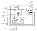
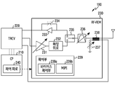
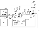
도 2a 내지 도 2d는 본 발명의 다양한 실시 예들에 따른 전자 장치에서 통신 모듈의 구성 예들이다.
도 3a는 본 발명의 다양한 실시 예들에 따른 전자 장치에서 매칭 회로의 예이다.
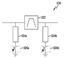
도 3b는 본 발명의 다양한 실시 예들에 따른 전자 장치에서 필터의 예이다.
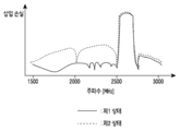
도 4는 본 발명의 다양한 실시 예들에 따른 전자 장치에서 필터의 조절에 의한 특성 변화의 예이다.
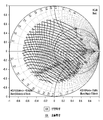
도 5는 본 발명의 다양한 실시 예들에 따른 전자 장치에서 매칭 회로의 임피던스 값의 조절에 의한 특성 변화의 예이다.
도 6은 본 발명의 다양한 실시 예들에 따른 전자 장치에서 매칭 회로의 임피던스 값의 조절에 의한 특성 변화의 다른 예이다.
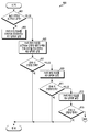
도 7은 본 발명의 다양한 실시 예들에 따른 전자 장치에서 네트워크에 따른 임피던스 조절을 위한 흐름도이다.
도 8은 본 발명의 다양한 실시 예들에 따른 전자 장치에서 네트워크에 따른 임피던스 조절을 위한 다른 흐름도이다.
도 9는 본 발명의 다양한 실시 예들에 따른 전자 장치에서 전력 증폭기의 예이다.
도 10은 본 발명의 다양한 실시 예들에 따른 전자 장치에서 전력 모드에 따른 전력 증폭기 및 임피던스 조절을 위한 흐름도이다.
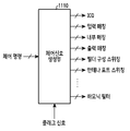
도 11은 본 발명의 다양한 실시 예들에 따른 전자 장치에서 신호를 처리하는 구성요소들의 상태 제어를 위한 제어 신호들을 생성하는 모듈의 예이다.
도 12는 본 발명의 다양한 실시 예들에 따른 전자 장치에서 전력 증폭기의 소손 방지를 위한 제어의 예이다.
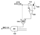
도 13a는 본 발명의 다양한 실시 예들에 따른 전자 장치에서 플래그 신호를 생성하는 회로의 구현 예이다.
도 13b 및 도 13c는 다양한 실시 예들에 따른 전자 장치에서 플래그 신호를 생성하는 회로에서 버퍼 및 비교기의 출력의 예들이다.
도 14는 본 발명의 다양한 실시 예들에 따른 전자 장치에서 신호를 처리하는 구성요소들의 상태를 제어하기 위한 흐름도이다.
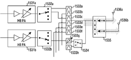
도 15는 본 발명의 다양한 실시 예들에 따른 전자 장치에서 복수의 안테나 구성들을 지원하기 위한 통신 모듈의 구성 예이다.
도 16은 본 발명의 다양한 실시 예들에 따른 전자 장치에서 CA(carrier aggregation) 동작의 활성 여부에 따라 안테나를 제어하기 위한 흐름도이다.
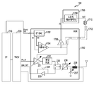
도 17은 본 발명의 다양한 실시 예들에 따른 전자 장치에서 ET(envelop tracking) 증폭 방식을 채택한 통신 모듈의 구성 예이다.
Claims (18)
- 전자 장치에 있어서,
송신 신호를 증폭하는 PA(power amplifier);
상기 PA와 연결되며, 부하 임피던스(load impedance)를 형성하는 매칭 회로;
상기 매칭 회로와 연결되는 필터; 및
상기 PA의 바이어스(bias), 상기 매칭 회로 또는 상기 필터 중 적어도 하나의 상태를 제어하는 제어 회로를 포함하며,
상기 제어 회로는, 제1 네트워크 및 제2 네트워크 중 상기 전자 장치가 접속된 네트워크를 식별하고, 상기 식별된 네트워크에 기반하여 상기 매칭 회로를 제1 상태, 제2 상태 또는 제3 상태 중 하나의 상태로 동작시키며,
상기 제1 상태는, 모듈 레벨에서 상기 제1 네트워크의 요구사항에 부합하는 선형성을 가지도록 정의된 상태이고,
상기 제2 상태는, 상기 모듈 레벨에서 상기 제2 네트워크의 요구사항에 부합하는 선형성을 가지도록 정의된 상태이고,
상기 제3 상태는, 상기 제1 상태보다 낮고 상기 제2 상태보다 높은 선형성을 제공하고, 상기 제1 상태보다 높고 상기 제2 상태보다 낮은 효율을 제공하는 상태인 전자 장치.
- 제1항에 있어서,
상기 제1 네트워크는, 상기 제2 네트워크보다 높은 선형성을 요구하는 네트워크이고,
상기 제어 회로는,
상기 식별된 네트워크가 상기 제1 네트워크인 경우, 상기 매칭 회로가 상기 제1 상태로 동작하도록 제어하고,
상기 식별된 네트워크가 상기 제2 네트워크인 경우, 상기 매칭 회로가 상기 제2 상태로 동작하도록 제어하는 전자 장치.
- 제1항에 있어서,
상기 제어 회로는, 상기 매칭 회로가 상기 제2 상태로 동작하도록 제어한 후, 상기 제2 상태로 동작하는 상황에서 측정된 선형성이 상기 제2 네트워크의 요구사항을 만족하지 못하면, 상기 매칭 회로를 상기 제3 상태로 동작하도록 제어하는 전자 장치.
- 제3항에 있어서,
상기 제어 회로는, 상기 매칭 회로가 상기 제3 상태로 동작하도록 제어한 후, 상기 제3 상태로 동작하는 상황에서 측정된 선형성이 상기 제2 네트워크의 요구사항을 만족하지 못하면, 상기 매칭 회로를 상기 제1 상태로 동작하도록 제어하는 전자 장치.
- 제3항에 있어서,
상기 제어 회로는, 상기 매칭 회로가 상기 제3 상태로 동작하도록 제어한 후, 상기 제3 상태로 동작하는 상황에서 측정된 선형성이 상기 제2 네트워크의 요구사항을 만족하지 못하면, 상기 매칭 회로를 제4 상태로 동작하도록 제어하며,
상기 제4 상태는, 상기 제1 상태보다 낮고 상기 제3 상태보다 높은 선형성을 제공하고, 상기 제1 상태보다 높고 상기 제3 상태보다 낮은 효율을 제공하는 상태인 전자 장치.
- 제1항에 있어서,
상기 필터를 통과한 송신 신호를 커플링하는 커플러를 더 포함하며,
상기 제어 회로는, 상기 커플러에 의해 커플링된 신호를 이용하여 운용 중 선형성을 측정하는 전자 장치.
- 제1항에 있어서,
디지털 포락선 신호를 아날로그 포락선 신호로 변환하는 DAC(digital to analog convertor);
상기 아날로그 포락선 신호에 기반하여 상기 PA에 인가되는 바이어스 신호의 일부를 생성하는 선형 레귤레이터;
상기 바이어스 신호의 나머지 일부를 생성하는 스위칭 레귤레이터; 및
상기 선형 레귤레이터의 출력 및 상기 스위칭 레귤레이터의 출력에 기반하여 상기 스위칭 레귤레이터의 스위칭 동작을 제어하는 신호를 생성하는 비교기를 더 포함하며,
상기 DAC, 상기 선형 레귤레이터, 상기 비교기는, 상기 PA와 동일한 모듈에 포함되는 전자 장치.
- 전자 장치에 있어서,
병렬로 연결된 복수의 증폭기들을 이용하여 송신 신호를 증폭하는 PA(power amplifier);
상기 PA와 연결되며, 부하 임피던스(load impedance)를 형성하는 매칭 회로; 및
상기 PA의 바이어스(bias) 또는 상기 매칭 회로의 상태를 제어하는 제어 회로를 포함하며,
상기 제어 회로는, 제1 전력 모드 및 제2 전력 모드 중 사용될 전력 모드를 식별하고, 상기 식별된 전력 모드에 기반하여 상기 PA에 포함된 증폭기들 중 온(on)되는 증폭기들의 개수를 조절하고, 상기 매칭 회로를 제1 상태, 제2 상태 또는 제3 상태 중 하나의 상태로 동작시키며,
상기 제1 상태는, 모듈 레벨에서 네트워크의 요구사항에 부합하는 선형성을 가지면서, 상기 매칭 회로가 제1 임피던스를 형성하도록 정의된 상태이고,
상기 제2 상태는, 상기 모듈 레벨에서 상기 네트워크의 요구사항에 부합하는 선형성을 가지면서, 상기 매칭 회로가 상기 제1 임피던스 보다 높은 제2 임피던스를 형성하도록 정의된 상태이고,
상기 제3 상태는, 상기 모듈 레벨에서 상기 네트워크의 요구사항에 부합하는 선형성을 가지면서, 상기 매칭 회로가 상기 제1 임피던스 보다 높고, 상기 제2 임피던스 보다 낮은 제3 임피던스를 형성하도록 정의된 상태인 전자 장치.
- 제8항에 있어서,
상기 제1 전력 모드는, 상기 제2 전력 모드보다 높은 송신 전력을 사용하는 모드이고,
상기 제어 회로는,
상기 식별된 전력 모드가 상기 제1 전력 모드인 경우, 상기 PA에 포함되는 증폭기들 전부가 온(on)되고, 상기 매칭 회로가 상기 제1 상태로 동작하도록 제어하고,
상기 식별된 전력 모드가 상기 제2 전력 모드인 경우, 상기 PA에 포함되는 증폭기들 중 제1 부분집합이 온(on)되고, 상기 매칭 회로가 상기 제2 상태로 동작하도록 제어하는 전자 장치.
- 제8항에 있어서,
상기 제어 회로는, 상기 매칭 회로가 상기 제2 상태로 동작하도록 제어한 후, 상기 제2 상태로 동작하는 상황에서 측정된 선형성이 네트워크의 요구사항을 만족하지 못하면, 상기 PA에 포함되는 증폭기들 중 제1 부분집합 보다 많은 개수의 증폭기들을 포함하는 제2 부분집합이 온(on)되고, 상기 매칭 회로를 상기 제3 상태로 동작하도록 제어하는 전자 장치.
- 제10항에 있어서,
상기 제어 회로는, 상기 매칭 회로가 상기 제3 상태로 동작하도록 제어한 후, 상기 제3 상태로 동작하는 상황에서 측정된 선형성이 네트워크의 요구사항을 만족하지 못하면, 상기 PA에 포함되는 증폭기들 중 모두가 온(on)되고, 상기 매칭 회로를 상기 제1 상태로 동작하도록 제어하는 전자 장치.
- 제10항에 있어서,
상기 제어 회로는, 상기 매칭 회로가 상기 제3 상태로 동작하도록 제어한 후, 상기 제3 상태로 동작하는 상황에서 측정된 선형성이 네트워크의 요구사항을 만족하지 못하면, 상기 PA에 포함되는 증폭기들 중 제2 부분집합 보다 많은 개수의 증폭기들을 포함하는 제3 부분집합이 온(on)되고, 상기 매칭 회로를 제4 상태로 동작하도록 제어하며,
상기 제4 상태는, 상기 제1 상태보다 높고 상기 제3 상태보다 낮은 임피던스를 형성하는 상태인 전자 장치.
- 제8항에 있어서,
디지털 포락선 신호를 아날로그 포락선 신호로 변환하는 DAC(digital to analog convertor);
상기 아날로그 포락선 신호에 기반하여 상기 PA에 인가되는 바이어스 신호의 일부를 생성하는 선형 레귤레이터;
상기 바이어스 신호의 나머지 일부를 생성하는 스위칭 레귤레이터; 및
상기 선형 레귤레이터의 출력 및 상기 스위칭 레귤레이터의 출력에 기반하여 상기 스위칭 레귤레이터의 스위칭 동작을 제어하는 신호를 생성하는 비교기를 더 포함하며,
상기 DAC, 상기 선형 레귤레이터, 상기 비교기는, 상기 PA와 동일한 모듈에 포함되는 전자 장치.
- 전자 장치에 있어서,
송신 신호를 증폭하는 PA(power amplifier);
상기 PA와 연결되며, 부하 임피던스(load impedance)를 형성하는 매칭 회로;
상기 매칭 회로와 연결되는 필터;
상기 필터와 연결되는 안테나 스위치; 및
상기 PA의 바이어스(bias), 상기 매칭 회로, 상기 필터, 상기 안테나 스위치의 상태를 제어하는 제어 회로를 포함하며,
상기 제어 회로는, 동작하고자 하는 모드로 천이하기 위해 상기 PA의 소손을 유발할 가능성이 있는 상태 조절이 필요한 경우, 상기 상태 조절 전 상기 PA의 바이어스를 미리 정의된 값으로 조절하고, 상기 상태 조절을 수행한 후, 상기 PA의 바이어스를 상기 모드에 따른 값으로 조절하는 전자 장치.
- 제14항에 있어서,
상기 PA의 소손을 유발할 가능성이 있는 상태 조절은, 상기 안테나 스위치의 조절, 또는 상기 필터에 포함된 스위치의 조절 중 적어도 하나를 포함하는 전자 장치.
- 제14항에 있어서,
상기 제어 회로는, 상기 상태 조절을 위한 제1 신호의 값 및 상기 상태 조절의 대상이 되는 구성요소에 인가되는 제2 신호의 값이 일치하게 된 후, 상기 PA의 바이어스를 상기 모드에 따른 값으로 조절하는 전자 장치.
- 제16항에 있어서,
상기 제어 회로는,
상기 상태 조절을 위한 상기 제1 신호를 출력하는 제어 신호 생성부;
상기 제1 신호에 기반하여 상기 상태 조절의 대상이 되는 구성요소에 인가되는 상기 제2 신호를 생성하는 버퍼;
상기 제2 신호를 기준 값과 비교하는 비교기;
상기 비교기의 출력 및 상기 제2 신호의 일치 시 긍정의 값을 가지는 신호를 출력하는 XNOR(exclusive non-or) 게이트를 포함하는 전자 장치.
- 제14항에 있어서,
디지털 포락선 신호를 아날로그 포락선 신호로 변환하는 DAC(digital to analog convertor);
상기 아날로그 포락선 신호에 기반하여 상기 PA에 인가되는 바이어스 신호의 일부를 생성하는 선형 레귤레이터;
상기 바이어스 신호의 나머지 일부를 생성하는 스위칭 레귤레이터; 및
상기 선형 레귤레이터의 출력 및 상기 스위칭 레귤레이터의 출력에 기반하여 상기 스위칭 레귤레이터의 스위칭 동작을 제어하는 신호를 생성하는 비교기를 더 포함하며,
상기 DAC, 상기 선형 레귤레이터, 상기 비교기는, 상기 PA와 동일한 모듈에 포함되는 전자 장치.
Priority Applications (5)
| Application Number | Priority Date | Filing Date | Title |
|---|---|---|---|
| KR1020190000812A KR102582479B1 (ko) | 2019-01-03 | 2019-01-03 | 무선 주파수 신호를 처리하는 모듈을 조절하기 위한 전자 장치 |
| PCT/KR2020/000129 WO2020141939A1 (en) | 2019-01-03 | 2020-01-03 | Electronic device for tuning module for processing radio frequency signal |
| CN202010007962.5A CN111404500B (zh) | 2019-01-03 | 2020-01-03 | 电子装置 |
| EP20150175.6A EP3678298B1 (en) | 2019-01-03 | 2020-01-03 | Electronic device for tuning module for processing radio frequency signal |
| US16/733,996 US11223332B2 (en) | 2019-01-03 | 2020-01-03 | Electronic device for tuning module for processing radio frequency signal |
Applications Claiming Priority (1)
| Application Number | Priority Date | Filing Date | Title |
|---|---|---|---|
| KR1020190000812A KR102582479B1 (ko) | 2019-01-03 | 2019-01-03 | 무선 주파수 신호를 처리하는 모듈을 조절하기 위한 전자 장치 |
Publications (2)
| Publication Number | Publication Date |
|---|---|
| KR20200084666A true KR20200084666A (ko) | 2020-07-13 |
| KR102582479B1 KR102582479B1 (ko) | 2023-09-25 |
Family
ID=69105743
Family Applications (1)
| Application Number | Title | Priority Date | Filing Date |
|---|---|---|---|
| KR1020190000812A Active KR102582479B1 (ko) | 2019-01-03 | 2019-01-03 | 무선 주파수 신호를 처리하는 모듈을 조절하기 위한 전자 장치 |
Country Status (5)
| Country | Link |
|---|---|
| US (1) | US11223332B2 (ko) |
| EP (1) | EP3678298B1 (ko) |
| KR (1) | KR102582479B1 (ko) |
| CN (1) | CN111404500B (ko) |
| WO (1) | WO2020141939A1 (ko) |
Families Citing this family (5)
| Publication number | Priority date | Publication date | Assignee | Title |
|---|---|---|---|---|
| US11539393B2 (en) | 2020-08-07 | 2022-12-27 | Apple Inc. | Radio-frequency front end modules with leakage management engines |
| CN112994736B (zh) * | 2021-02-07 | 2022-05-06 | 锐石创芯(深圳)科技股份有限公司 | 一种射频前端模块及天线装置 |
| US11956108B2 (en) * | 2021-06-14 | 2024-04-09 | Skyworks Solutions, Inc. | Antenna swapping without blanking symbols |
| US12519499B2 (en) | 2022-10-26 | 2026-01-06 | Hewlett Packard Enterprise Development Lp | Short detection and protection circuit for access point |
| KR20240078796A (ko) * | 2022-11-28 | 2024-06-04 | 삼성전자주식회사 | 무선 주파수 프런트 엔드의 손상을 방지할 수 있는 전자 장치와 이를 포함하는 전자 시스템 |
Citations (4)
| Publication number | Priority date | Publication date | Assignee | Title |
|---|---|---|---|---|
| US7202734B1 (en) * | 1999-07-06 | 2007-04-10 | Frederick Herbert Raab | Electronically tuned power amplifier |
| US20120169565A1 (en) * | 2010-08-26 | 2012-07-05 | Morris Iii Arthur S | Tunable radio front end and methods |
| KR20130066558A (ko) * | 2010-11-11 | 2013-06-20 | 리서치 인 모션 알에프, 인크. | 통신 장치의 동작을 관리하는 방법 및 장치 |
| US20140167856A1 (en) * | 2011-09-15 | 2014-06-19 | Murata Manufacturing Co., Ltd. | Power amplifier and operation method therefor |
Family Cites Families (24)
| Publication number | Priority date | Publication date | Assignee | Title |
|---|---|---|---|---|
| US6281748B1 (en) | 2000-01-14 | 2001-08-28 | Motorola, Inc. | Method of and apparatus for modulation dependent signal amplification |
| US6680652B2 (en) * | 2001-08-06 | 2004-01-20 | Rf Micro Devices, Inc. | Load switching for transmissions with different peak-to-average power ratios |
| US6614309B1 (en) | 2002-02-21 | 2003-09-02 | Ericsson Inc. | Dynamic bias controller for power amplifier circuits |
| US7355470B2 (en) | 2006-04-24 | 2008-04-08 | Parkervision, Inc. | Systems and methods of RF power transmission, modulation, and amplification, including embodiments for amplifier class transitioning |
| US8588727B2 (en) * | 2008-03-21 | 2013-11-19 | Qualcomm Incorporated | Adaptive linearity communication device |
| US9026062B2 (en) * | 2009-10-10 | 2015-05-05 | Blackberry Limited | Method and apparatus for managing operations of a communication device |
| US8738066B2 (en) * | 2010-10-07 | 2014-05-27 | Apple Inc. | Wireless transceiver with amplifier bias adjusted based on modulation scheme and transmit power feedback |
| US8611834B2 (en) * | 2010-11-01 | 2013-12-17 | Cree, Inc. | Matching network for transmission circuitry |
| US8908751B2 (en) | 2011-02-28 | 2014-12-09 | Intel Mobile Communications GmbH | Joint adaptive bias point adjustment and digital pre-distortion for power amplifier |
| US8767871B2 (en) * | 2011-06-08 | 2014-07-01 | Broadcom Corporation | Antenna tuning using the ratio of complex forward and reflected signals |
| CN102752007B (zh) | 2012-06-28 | 2015-02-11 | 惠州Tcl移动通信有限公司 | 一种用于自动调节天线匹配的移动终端及其控制方法 |
| US20140028521A1 (en) * | 2012-07-27 | 2014-01-30 | Rf Micro Devices, Inc. | Tuner topology for wide bandwidth |
| US8897730B2 (en) * | 2012-12-31 | 2014-11-25 | Triquint Semiconductor, Inc. | Radio frequency switch circuit |
| US9049664B2 (en) * | 2013-06-24 | 2015-06-02 | Mediatek Inc. | Wireless communications circuit for improving current consumption and RF performance |
| CN103532503A (zh) * | 2013-09-18 | 2014-01-22 | 清华大学 | 功率放大器 |
| US9661440B2 (en) | 2014-07-25 | 2017-05-23 | Qualcomm Incorporated | Methods and systems for triggering efficient application synchronization |
| WO2016195859A1 (en) * | 2015-05-29 | 2016-12-08 | Rf Micro Devices, Inc. | Linear power amplifier |
| US9806676B2 (en) | 2015-07-28 | 2017-10-31 | Skyworks Solutions, Inc. | Power amplification system with programmable load line |
| US10128872B2 (en) | 2015-08-26 | 2018-11-13 | Intel IP Corporation | Enabling radio frequency multiplexing in a wireless system |
| US10050591B2 (en) * | 2016-03-23 | 2018-08-14 | Cree, Inc. | LC network for a power amplifier with selectable impedance |
| KR102496907B1 (ko) | 2016-06-16 | 2023-02-08 | 삼성전자주식회사 | 안테나 및 안테나를 포함하는 전자 장치 |
| US10164587B2 (en) | 2016-11-03 | 2018-12-25 | Qorvo Us, Inc. | Electronically reconfigurable matching network |
| US10122326B2 (en) | 2016-11-04 | 2018-11-06 | Qualcomm Incorporated | Systems and methods providing loadline modulation of a power amplifier |
| WO2018162746A1 (en) * | 2017-03-10 | 2018-09-13 | Acco | Power amplifier with stepwise envelope tracking and adaptive load |
-
2019
- 2019-01-03 KR KR1020190000812A patent/KR102582479B1/ko active Active
-
2020
- 2020-01-03 US US16/733,996 patent/US11223332B2/en active Active
- 2020-01-03 CN CN202010007962.5A patent/CN111404500B/zh not_active Expired - Fee Related
- 2020-01-03 EP EP20150175.6A patent/EP3678298B1/en active Active
- 2020-01-03 WO PCT/KR2020/000129 patent/WO2020141939A1/en not_active Ceased
Patent Citations (4)
| Publication number | Priority date | Publication date | Assignee | Title |
|---|---|---|---|---|
| US7202734B1 (en) * | 1999-07-06 | 2007-04-10 | Frederick Herbert Raab | Electronically tuned power amplifier |
| US20120169565A1 (en) * | 2010-08-26 | 2012-07-05 | Morris Iii Arthur S | Tunable radio front end and methods |
| KR20130066558A (ko) * | 2010-11-11 | 2013-06-20 | 리서치 인 모션 알에프, 인크. | 통신 장치의 동작을 관리하는 방법 및 장치 |
| US20140167856A1 (en) * | 2011-09-15 | 2014-06-19 | Murata Manufacturing Co., Ltd. | Power amplifier and operation method therefor |
Also Published As
| Publication number | Publication date |
|---|---|
| CN111404500A (zh) | 2020-07-10 |
| KR102582479B1 (ko) | 2023-09-25 |
| CN111404500B (zh) | 2023-10-20 |
| EP3678298B1 (en) | 2022-06-29 |
| WO2020141939A1 (en) | 2020-07-09 |
| US11223332B2 (en) | 2022-01-11 |
| EP3678298A1 (en) | 2020-07-08 |
| US20200220506A1 (en) | 2020-07-09 |
Similar Documents
| Publication | Publication Date | Title |
|---|---|---|
| KR102773503B1 (ko) | 전력증폭기 소손 방지를 위한 전압 보호 회로 및 이를 포함하는 전자 장치 | |
| CN113169715B (zh) | 电子装置中的保护电路及其方法 | |
| US11223332B2 (en) | Electronic device for tuning module for processing radio frequency signal | |
| US10958219B2 (en) | Method and device for selectively supplying voltage to multiple amplifiers by using switching regulators | |
| KR102556360B1 (ko) | 제어 정보 에 기반하여 송신 전력을 제어하기 위한 전자 장치 및 방법 | |
| KR102538889B1 (ko) | 통신 열화를 방지하기 위한 전자 장치 및 그 제어 방법 | |
| KR20200108546A (ko) | 통신을 위한 주파수 대역을 제어하기 위한 방법 및 그 전자 장치 | |
| US12580600B2 (en) | Transmission device and electronic device including same | |
| US11183972B2 (en) | Method for adjusting output of amplifier by using sensing circuit configured to sense power supplied to amplifier and electronic device therefor | |
| KR102904531B1 (ko) | 송신 신호 증폭을 위한 인가 전압 조절 방법 및 그 전자 장치 | |
| KR20220142287A (ko) | 보호 회로를 포함하는 전력 증폭 회로, 및 전력 증폭 회로를 포함하는 전자 장치 | |
| KR102573284B1 (ko) | 신호의 대역폭에 따라 안테나 설정을 변경하는 전자 장치 및 제어 방법 | |
| KR20200093938A (ko) | 안테나의 임피던스 운용 방법 및 그 전자 장치 | |
| US12424984B2 (en) | Power amplification circuit including protection circuit and electronic device including power amplification circuit | |
| US20250007542A1 (en) | Electronic device adaptively changing power supply circuit connected to power amplifier for transmit power of signal | |
| KR20260013860A (ko) | 반사 계수에 기반하여 안테나 상태를 확인하는 전자 장치, 방법, 및 비 일시적 컴퓨터 판독가능 저장 매체 | |
| KR20260018648A (ko) | Rf 신호를 송신하기 위한 전자 장치 및 그 동작 방법과 저장 매체 | |
| KR20260002090A (ko) | 전원 공급 회로 및 이를 포함하는 전자 장치 | |
| KR20210126981A (ko) | 스위치 및 스위치를 포함하는 전자 장치 |
Legal Events
| Date | Code | Title | Description |
|---|---|---|---|
| PA0109 | Patent application |
Patent event code: PA01091R01D Comment text: Patent Application Patent event date: 20190103 |
|
| PG1501 | Laying open of application | ||
| A201 | Request for examination | ||
| PA0201 | Request for examination |
Patent event code: PA02012R01D Patent event date: 20220103 Comment text: Request for Examination of Application Patent event code: PA02011R01I Patent event date: 20190103 Comment text: Patent Application |
|
| E902 | Notification of reason for refusal | ||
| PE0902 | Notice of grounds for rejection |
Comment text: Notification of reason for refusal Patent event date: 20221208 Patent event code: PE09021S01D |
|
| E701 | Decision to grant or registration of patent right | ||
| PE0701 | Decision of registration |
Patent event code: PE07011S01D Comment text: Decision to Grant Registration Patent event date: 20230622 |
|
| GRNT | Written decision to grant | ||
| PR0701 | Registration of establishment |
Comment text: Registration of Establishment Patent event date: 20230920 Patent event code: PR07011E01D |
|
| PR1002 | Payment of registration fee |
Payment date: 20230921 End annual number: 3 Start annual number: 1 |
|
| PG1601 | Publication of registration |