KR20200087384A - 표시 장치 - Google Patents
표시 장치 Download PDFInfo
- Publication number
- KR20200087384A KR20200087384A KR1020190003450A KR20190003450A KR20200087384A KR 20200087384 A KR20200087384 A KR 20200087384A KR 1020190003450 A KR1020190003450 A KR 1020190003450A KR 20190003450 A KR20190003450 A KR 20190003450A KR 20200087384 A KR20200087384 A KR 20200087384A
- Authority
- KR
- South Korea
- Prior art keywords
- pixel
- area
- display device
- display area
- electrode
- Prior art date
- Legal status (The legal status is an assumption and is not a legal conclusion. Google has not performed a legal analysis and makes no representation as to the accuracy of the status listed.)
- Granted
Links
Images










Classifications
-
- G—PHYSICS
- G09—EDUCATION; CRYPTOGRAPHY; DISPLAY; ADVERTISING; SEALS
- G09G—ARRANGEMENTS OR CIRCUITS FOR CONTROL OF INDICATING DEVICES USING STATIC MEANS TO PRESENT VARIABLE INFORMATION
- G09G3/00—Control arrangements or circuits, of interest only in connection with visual indicators other than cathode-ray tubes
- G09G3/20—Control arrangements or circuits, of interest only in connection with visual indicators other than cathode-ray tubes for presentation of an assembly of a number of characters, e.g. a page, by composing the assembly by combination of individual elements arranged in a matrix no fixed position being assigned to or needed to be assigned to the individual characters or partial characters
- G09G3/22—Control arrangements or circuits, of interest only in connection with visual indicators other than cathode-ray tubes for presentation of an assembly of a number of characters, e.g. a page, by composing the assembly by combination of individual elements arranged in a matrix no fixed position being assigned to or needed to be assigned to the individual characters or partial characters using controlled light sources
- G09G3/30—Control arrangements or circuits, of interest only in connection with visual indicators other than cathode-ray tubes for presentation of an assembly of a number of characters, e.g. a page, by composing the assembly by combination of individual elements arranged in a matrix no fixed position being assigned to or needed to be assigned to the individual characters or partial characters using controlled light sources using electroluminescent panels
- G09G3/32—Control arrangements or circuits, of interest only in connection with visual indicators other than cathode-ray tubes for presentation of an assembly of a number of characters, e.g. a page, by composing the assembly by combination of individual elements arranged in a matrix no fixed position being assigned to or needed to be assigned to the individual characters or partial characters using controlled light sources using electroluminescent panels semiconductive, e.g. using light-emitting diodes [LED]
- G09G3/3208—Control arrangements or circuits, of interest only in connection with visual indicators other than cathode-ray tubes for presentation of an assembly of a number of characters, e.g. a page, by composing the assembly by combination of individual elements arranged in a matrix no fixed position being assigned to or needed to be assigned to the individual characters or partial characters using controlled light sources using electroluminescent panels semiconductive, e.g. using light-emitting diodes [LED] organic, e.g. using organic light-emitting diodes [OLED]
-
- H01L27/3276—
-
- G—PHYSICS
- G09—EDUCATION; CRYPTOGRAPHY; DISPLAY; ADVERTISING; SEALS
- G09G—ARRANGEMENTS OR CIRCUITS FOR CONTROL OF INDICATING DEVICES USING STATIC MEANS TO PRESENT VARIABLE INFORMATION
- G09G3/00—Control arrangements or circuits, of interest only in connection with visual indicators other than cathode-ray tubes
- G09G3/20—Control arrangements or circuits, of interest only in connection with visual indicators other than cathode-ray tubes for presentation of an assembly of a number of characters, e.g. a page, by composing the assembly by combination of individual elements arranged in a matrix no fixed position being assigned to or needed to be assigned to the individual characters or partial characters
- G09G3/22—Control arrangements or circuits, of interest only in connection with visual indicators other than cathode-ray tubes for presentation of an assembly of a number of characters, e.g. a page, by composing the assembly by combination of individual elements arranged in a matrix no fixed position being assigned to or needed to be assigned to the individual characters or partial characters using controlled light sources
- G09G3/30—Control arrangements or circuits, of interest only in connection with visual indicators other than cathode-ray tubes for presentation of an assembly of a number of characters, e.g. a page, by composing the assembly by combination of individual elements arranged in a matrix no fixed position being assigned to or needed to be assigned to the individual characters or partial characters using controlled light sources using electroluminescent panels
- G09G3/32—Control arrangements or circuits, of interest only in connection with visual indicators other than cathode-ray tubes for presentation of an assembly of a number of characters, e.g. a page, by composing the assembly by combination of individual elements arranged in a matrix no fixed position being assigned to or needed to be assigned to the individual characters or partial characters using controlled light sources using electroluminescent panels semiconductive, e.g. using light-emitting diodes [LED]
- G09G3/3208—Control arrangements or circuits, of interest only in connection with visual indicators other than cathode-ray tubes for presentation of an assembly of a number of characters, e.g. a page, by composing the assembly by combination of individual elements arranged in a matrix no fixed position being assigned to or needed to be assigned to the individual characters or partial characters using controlled light sources using electroluminescent panels semiconductive, e.g. using light-emitting diodes [LED] organic, e.g. using organic light-emitting diodes [OLED]
- G09G3/3225—Control arrangements or circuits, of interest only in connection with visual indicators other than cathode-ray tubes for presentation of an assembly of a number of characters, e.g. a page, by composing the assembly by combination of individual elements arranged in a matrix no fixed position being assigned to or needed to be assigned to the individual characters or partial characters using controlled light sources using electroluminescent panels semiconductive, e.g. using light-emitting diodes [LED] organic, e.g. using organic light-emitting diodes [OLED] using an active matrix
- G09G3/3233—Control arrangements or circuits, of interest only in connection with visual indicators other than cathode-ray tubes for presentation of an assembly of a number of characters, e.g. a page, by composing the assembly by combination of individual elements arranged in a matrix no fixed position being assigned to or needed to be assigned to the individual characters or partial characters using controlled light sources using electroluminescent panels semiconductive, e.g. using light-emitting diodes [LED] organic, e.g. using organic light-emitting diodes [OLED] using an active matrix with pixel circuitry controlling the current through the light-emitting element
-
- G—PHYSICS
- G09—EDUCATION; CRYPTOGRAPHY; DISPLAY; ADVERTISING; SEALS
- G09G—ARRANGEMENTS OR CIRCUITS FOR CONTROL OF INDICATING DEVICES USING STATIC MEANS TO PRESENT VARIABLE INFORMATION
- G09G3/00—Control arrangements or circuits, of interest only in connection with visual indicators other than cathode-ray tubes
- G09G3/20—Control arrangements or circuits, of interest only in connection with visual indicators other than cathode-ray tubes for presentation of an assembly of a number of characters, e.g. a page, by composing the assembly by combination of individual elements arranged in a matrix no fixed position being assigned to or needed to be assigned to the individual characters or partial characters
- G09G3/34—Control arrangements or circuits, of interest only in connection with visual indicators other than cathode-ray tubes for presentation of an assembly of a number of characters, e.g. a page, by composing the assembly by combination of individual elements arranged in a matrix no fixed position being assigned to or needed to be assigned to the individual characters or partial characters by control of light from an independent source
- G09G3/36—Control arrangements or circuits, of interest only in connection with visual indicators other than cathode-ray tubes for presentation of an assembly of a number of characters, e.g. a page, by composing the assembly by combination of individual elements arranged in a matrix no fixed position being assigned to or needed to be assigned to the individual characters or partial characters by control of light from an independent source using liquid crystals
- G09G3/3607—Control arrangements or circuits, of interest only in connection with visual indicators other than cathode-ray tubes for presentation of an assembly of a number of characters, e.g. a page, by composing the assembly by combination of individual elements arranged in a matrix no fixed position being assigned to or needed to be assigned to the individual characters or partial characters by control of light from an independent source using liquid crystals for displaying colours or for displaying grey scales with a specific pixel layout, e.g. using sub-pixels
-
- G—PHYSICS
- G09—EDUCATION; CRYPTOGRAPHY; DISPLAY; ADVERTISING; SEALS
- G09G—ARRANGEMENTS OR CIRCUITS FOR CONTROL OF INDICATING DEVICES USING STATIC MEANS TO PRESENT VARIABLE INFORMATION
- G09G3/00—Control arrangements or circuits, of interest only in connection with visual indicators other than cathode-ray tubes
- G09G3/20—Control arrangements or circuits, of interest only in connection with visual indicators other than cathode-ray tubes for presentation of an assembly of a number of characters, e.g. a page, by composing the assembly by combination of individual elements arranged in a matrix no fixed position being assigned to or needed to be assigned to the individual characters or partial characters
- G09G3/34—Control arrangements or circuits, of interest only in connection with visual indicators other than cathode-ray tubes for presentation of an assembly of a number of characters, e.g. a page, by composing the assembly by combination of individual elements arranged in a matrix no fixed position being assigned to or needed to be assigned to the individual characters or partial characters by control of light from an independent source
- G09G3/36—Control arrangements or circuits, of interest only in connection with visual indicators other than cathode-ray tubes for presentation of an assembly of a number of characters, e.g. a page, by composing the assembly by combination of individual elements arranged in a matrix no fixed position being assigned to or needed to be assigned to the individual characters or partial characters by control of light from an independent source using liquid crystals
- G09G3/3611—Control of matrices with row and column drivers
- G09G3/3674—Details of drivers for scan electrodes
- G09G3/3677—Details of drivers for scan electrodes suitable for active matrices only
-
- H01L27/3216—
-
- H01L51/52—
-
- H—ELECTRICITY
- H10—SEMICONDUCTOR DEVICES; ELECTRIC SOLID-STATE DEVICES NOT OTHERWISE PROVIDED FOR
- H10K—ORGANIC ELECTRIC SOLID-STATE DEVICES
- H10K59/00—Integrated devices, or assemblies of multiple devices, comprising at least one organic light-emitting element covered by group H10K50/00
- H10K59/10—OLED displays
- H10K59/12—Active-matrix OLED [AMOLED] displays
- H10K59/121—Active-matrix OLED [AMOLED] displays characterised by the geometry or disposition of pixel elements
-
- H—ELECTRICITY
- H10—SEMICONDUCTOR DEVICES; ELECTRIC SOLID-STATE DEVICES NOT OTHERWISE PROVIDED FOR
- H10K—ORGANIC ELECTRIC SOLID-STATE DEVICES
- H10K59/00—Integrated devices, or assemblies of multiple devices, comprising at least one organic light-emitting element covered by group H10K50/00
- H10K59/10—OLED displays
- H10K59/12—Active-matrix OLED [AMOLED] displays
- H10K59/131—Interconnections, e.g. wiring lines or terminals
-
- H—ELECTRICITY
- H10—SEMICONDUCTOR DEVICES; ELECTRIC SOLID-STATE DEVICES NOT OTHERWISE PROVIDED FOR
- H10K—ORGANIC ELECTRIC SOLID-STATE DEVICES
- H10K59/00—Integrated devices, or assemblies of multiple devices, comprising at least one organic light-emitting element covered by group H10K50/00
- H10K59/30—Devices specially adapted for multicolour light emission
- H10K59/35—Devices specially adapted for multicolour light emission comprising red-green-blue [RGB] subpixels
- H10K59/352—Devices specially adapted for multicolour light emission comprising red-green-blue [RGB] subpixels the areas of the RGB subpixels being different
-
- G—PHYSICS
- G09—EDUCATION; CRYPTOGRAPHY; DISPLAY; ADVERTISING; SEALS
- G09G—ARRANGEMENTS OR CIRCUITS FOR CONTROL OF INDICATING DEVICES USING STATIC MEANS TO PRESENT VARIABLE INFORMATION
- G09G2300/00—Aspects of the constitution of display devices
- G09G2300/04—Structural and physical details of display devices
- G09G2300/0421—Structural details of the set of electrodes
- G09G2300/0426—Layout of electrodes and connections
-
- G—PHYSICS
- G09—EDUCATION; CRYPTOGRAPHY; DISPLAY; ADVERTISING; SEALS
- G09G—ARRANGEMENTS OR CIRCUITS FOR CONTROL OF INDICATING DEVICES USING STATIC MEANS TO PRESENT VARIABLE INFORMATION
- G09G2320/00—Control of display operating conditions
- G09G2320/06—Adjustment of display parameters
- G09G2320/0686—Adjustment of display parameters with two or more screen areas displaying information with different brightness or colours
-
- G—PHYSICS
- G09—EDUCATION; CRYPTOGRAPHY; DISPLAY; ADVERTISING; SEALS
- G09G—ARRANGEMENTS OR CIRCUITS FOR CONTROL OF INDICATING DEVICES USING STATIC MEANS TO PRESENT VARIABLE INFORMATION
- G09G2340/00—Aspects of display data processing
- G09G2340/04—Changes in size, position or resolution of an image
- G09G2340/0407—Resolution change, inclusive of the use of different resolutions for different screen areas
-
- H—ELECTRICITY
- H10—SEMICONDUCTOR DEVICES; ELECTRIC SOLID-STATE DEVICES NOT OTHERWISE PROVIDED FOR
- H10K—ORGANIC ELECTRIC SOLID-STATE DEVICES
- H10K59/00—Integrated devices, or assemblies of multiple devices, comprising at least one organic light-emitting element covered by group H10K50/00
- H10K59/60—OLEDs integrated with inorganic light-sensitive elements, e.g. with inorganic solar cells or inorganic photodiodes
- H10K59/65—OLEDs integrated with inorganic image sensors
-
- H—ELECTRICITY
- H10—SEMICONDUCTOR DEVICES; ELECTRIC SOLID-STATE DEVICES NOT OTHERWISE PROVIDED FOR
- H10K—ORGANIC ELECTRIC SOLID-STATE DEVICES
- H10K59/00—Integrated devices, or assemblies of multiple devices, comprising at least one organic light-emitting element covered by group H10K50/00
- H10K59/80—Constructional details
Landscapes
- Engineering & Computer Science (AREA)
- Physics & Mathematics (AREA)
- Computer Hardware Design (AREA)
- General Physics & Mathematics (AREA)
- Theoretical Computer Science (AREA)
- Microelectronics & Electronic Packaging (AREA)
- Chemical & Material Sciences (AREA)
- Inorganic Chemistry (AREA)
- Crystallography & Structural Chemistry (AREA)
- Life Sciences & Earth Sciences (AREA)
- Sustainable Development (AREA)
- Geometry (AREA)
- Devices For Indicating Variable Information By Combining Individual Elements (AREA)
- Electroluminescent Light Sources (AREA)
- Optics & Photonics (AREA)
- Liquid Crystal (AREA)
Abstract
Description
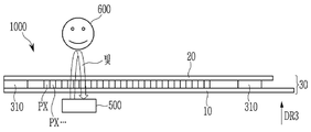
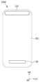
도 4는 한 실시예에 따른 표시 장치의 개략적인 단면도이다.
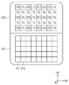
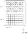
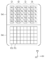
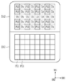
도 5 내지 도 12는 각각 한 실시예에 따른 표시 장치의 제1 표시 영역과 제2 표시 영역의 배치도이다.
도 13은 한 실시예에 따른 표시 장치의 표시 영역의 배치도이다.
도 14는 도 13에 도시한 표시 장치를 XIV-XIV'선을 따라 잘라 도시한 단면도이다.
도 15는 제2 표시 영역의 화소 영역 및 광투과 영역을 도시한 것이다.
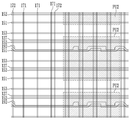
도 16은 본 발명의 일 실시예에 따른 표시 장치의 제2 표시 영역을 도시한 것이다.
도 17은 제어선만 제거된 실시예를 도시한 것이다.
도 18은 제1 스캔선만 제거된 실시예를 도시한 것이다.
도 19는 다른 일 실시예에 따른 표시 장치에 대하여 제2 표시 영역을 도시한 것이다.
도 20, 도 21 및 도 22는 다른 실시예에 따른 표시 장치를 도시한 것이다
도 23은 도 19 내지 도 22의 실시예에 따른 표시 장치에서 구동부와 제2 표시 영역을 도시한 것이다
도 24는 본 발명의 일 실시예에 따른 표시 장치를 도시한 것이다.
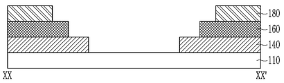
도 25는 도 24의 XX-XX'선을 따라 자른 단면도를 도시한 것이다.
도 26은 본 발명의 다른 일 실시예에 대하여 도 25와 동일한 단면을 도시한 것이다.
도 27은 다른 일 실시예에 따른 표시 장치의 제2 표시 영역을 도시한 것이다.
도 28은 일 실시예에 따른 표시 장치의 제2 표시 영역을 도시한 것이다.
도 29는 도 28의 화소 영역을 보다 자세하게 도시한 것이다.
Claims (25)
- 복수의 제1 화소 영역을 포함하는 제1 표시 영역, 그리고
복수의 제2 화소 영역 및 복수의 광투과 영역을 포함하는 제2 표시 영역을 포함하고,
상기 제2 표시 영역은 복수의 스캔선을 포함하고,
상기 제2 화소 영역은 복수의 화소 전극 및 상기 화소 전극과 동일 층에 위치하는 전압선을 포함하고,
상기 광투과 영역에서 상기 전압선은 상기 스캔선과 중첩하여 나란하게 위치하는 표시 장치. - 제1항에서,
상기 광투과 영역에는 화소 전극이 위치하지 않는 표시 장치. - 제1항에서,
상기 제2 표시 영역은 제어선을 더 포함하고,
상기 광투과 영역에서 상기 복수의 스캔선 및 제어선 중 일부가 제거되어 있는 표시 장치. - 제3항에서,
상기 복수의 스캔선은 제1 스캔선 및 제2 스캔선을 포함하고,
상기 제1 스캔선 중 일부는 이웃하는 화소 열의 제2 스캔선과 연결되어 있는 표시 장치. - 제3항에서,
상기 제어선 중 일부는 이웃하는 화소 열의 제어선과 연결되어 있는 표시 장치. - 제1항에서,
상기 제2 표시 영역은 복수의 데이터선 및 구동 전압선을 포함하고,
상기 광투과 영역에서 상기 구동 전압선의 일부가 제거되어 있는 표시 장치. - 제6항에서,
상기 광투과 영역에서 상기 데이터선 일부가 제거되어 있는 표시 장치. - 제6항에서,
상기 표시 장치는 구동부를 더 포함하고,
상기 구동부와 상기 제2 표시 영역 사이에 상기 제1 표시 영역이 위치하는 표시 장치. - 제1항에서,
상기 제2 표시 영역은 복수의 배선을 포함하고,
상기 배선은 제1 방향으로 위치하는 복수의 스캔선 및 제어선, 제2 방향으로 위치하는 복수의 데이터선 및 구동 전압선을 포함하고,
상기 광투과 영역에서 상기 배선의 일부는 구부러져 서로 가까이 위치하는 표시 장치. - 제9항에서,
상기 광투과 영역에서의 일부 배선 사이의 간격이 상기 제2 화소 영역에서의 배선 사이의 간격보다 좁은 표시 장치. - 제9항에서,
상기 광투과 영역 중 상기 배선이 위치하지 않는 영역은, 무기막 및 유기막이 일부 제거된 개구부를 갖는 표시 장치. - 복수의 제1 화소 영역을 포함하는 제1 표시 영역, 그리고
복수의 제2 화소 영역 및 복수의 광투과 영역을 포함하는 제2 표시 영역을 포함하고,
상기 제2 표시 영역은 복수의 배선을 포함하고,
상기 배선은 제1 방향으로 위치하는 복수의 스캔선 및 제어선, 제2 방향으로 위치하는 복수의 데이터선 및 구동 전압선을 포함하고
상기 광투과 영역에서 상기 복수의 배선 중 하나 이상이 제거된 표시 장치. - 제12항에서,
상기 광투과 영역에서 상기 배선의 일부는 구부러져 서로 가까이 위치하는 표시 장치. - 제13항에서,
상기 광투과 영역에서의 상기 일부 배선 사이의 간격이 상기 제2 화소 영역에서의 배선 사이의 간격보다 좁은 표시 장치. - 제14항에서,
상기 광투과 영역 중 상기 배선이 위치하지 않는 영역은, 무기막 및 유기막이 일부 제거된 개구부를 갖는 표시 장치. - 제12항에서,
상기 제2 화소 영역은 복수의 화소 전극을 포함하고,
상기 제2 화소 영역은 상기 화소 전극과 동일 층에 위치하는 전압선을 포함하지 않고,
각각의 화소 전극은 광투과 영역과 중첩하지 않는 표시 장치. - 제12항에서,
상기 표시 장치는 구동부를 더 포함하고,
상기 구동부와 상기 제2 표시 영역 사이에 상기 제1 표시 영역이 위치하는 표시 장치. - 복수의 제1 화소 영역을 포함하는 제1 표시 영역, 그리고
복수의 제2 화소 영역 및 복수의 광투과 영역을 포함하는 제2 표시 영역을 포함하고,
상기 제2 표시 영역은 복수의 배선을 포함하고,
상기 배선은 제1 방향으로 위치하는 복수의 스캔선 및 제어선, 제2 방향으로 위치하는 복수의 데이터선 및 구동 전압선을 포함하고
상기 광투과 영역에서 상기 배선의 일부는 구부러져 있으며,
상기 광투과 영역에서의 일부 배선 사이의 간격이 상기 제2 화소 영역에서의 배선 사이의 간격보다 좁은 표시 장치. - 제18항에서,
상기 광투과 영역 중 상기 배선이 위치하지 않는 영역은, 무기막 및 유기막이 일부 제거된 개구부를 갖는 표시 장치. - 제18항에서,
상기 제2 화소 영역은 복수의 화소 전극을 포함하고,
상기 제2 화소 영역은 상기 화소 전극과 동일 층에 위치하는 전압선을 포함하지 않고,
각각의 화소 전극은 광투과 영역과 중첩하지 않는 표시 장치. - 제18항에서,
상기 광투과 영역에는 화소 전극이 위치하지 않는 표시 장치. - 복수의 제1 화소 영역을 포함하는 제1 표시 영역, 그리고
복수의 제2 화소 영역 및 복수의 광투과 영역을 포함하는 제2 표시 영역을 포함하고,
상기 광투과 영역에는 화소 전극이 위치하지 않으며,
상기 제2 화소 영역은 복수의 트랜지스터 및 복수의 화소 전극을 포함하고,
상기 복수의 트랜지스터는
스위칭 트랜지스터;
구동 트랜지스터, 및
상기 구동 트랜지스터의 출력측 전극과 연결되어 있는 제1 전극 및 상기 구동 트랜지스터의 게이트 전극과 연결되어 있는 제2 전극을 포함하는 제3 트랜지스터를 포함하며,
각각의 화소 전극은 상기 제3 트랜지스터와 중첩하여 위치하는 표시 장치. - 제22항에서,
상기 각각의 화소 전극은 광투과 영역과 중첩하지 않는 표시 장치. - 제22항에서,
상기 표시 장치는 상기 화소 전극과 동일 층에 위치하는 전압선을 포함하지 않는 표시 장치. - 제22항에서,
상기 복수의 화소 전극은 제1 화소 전극, 제2 화소 전극 및 제3 화소 전극을 포함하고,
상기 제2 화소 영역은 제1 방향으로 나란하게 위치하는 제1 스캔선, 제2 스캔선 및 제어선을 포함하고,
상기 제1 화소 전극 및 상기 제3 화소 전극은 상기 제1 스캔선과 상기 제어선 사이에서 제1 방향으로의 폭이 가장 넓은 평면 형상을 가지고,
상기 제2 화소 전극은 상기 제2 스캔선과 중첩하는 영역에서 제1 방향으로의 폭이 가장 넓은 평면 형상을 갖는 표시 장치.
Priority Applications (5)
| Application Number | Priority Date | Filing Date | Title |
|---|---|---|---|
| KR1020190003450A KR102792464B1 (ko) | 2019-01-10 | 2019-01-10 | 표시 장치 |
| EP20150855.3A EP3680888A1 (en) | 2019-01-10 | 2020-01-09 | Display device having light transmissive regions |
| US16/739,714 US11411062B2 (en) | 2019-01-10 | 2020-01-10 | Display device having light transmissive regions |
| CN202010024375.7A CN111429838B (zh) | 2019-01-10 | 2020-01-10 | 具有透光区域的显示装置 |
| US17/813,592 US20220359641A1 (en) | 2019-01-10 | 2022-07-19 | Display device having light transmissive regions |
Applications Claiming Priority (1)
| Application Number | Priority Date | Filing Date | Title |
|---|---|---|---|
| KR1020190003450A KR102792464B1 (ko) | 2019-01-10 | 2019-01-10 | 표시 장치 |
Publications (2)
| Publication Number | Publication Date |
|---|---|
| KR20200087384A true KR20200087384A (ko) | 2020-07-21 |
| KR102792464B1 KR102792464B1 (ko) | 2025-04-07 |
Family
ID=69156267
Family Applications (1)
| Application Number | Title | Priority Date | Filing Date |
|---|---|---|---|
| KR1020190003450A Active KR102792464B1 (ko) | 2019-01-10 | 2019-01-10 | 표시 장치 |
Country Status (4)
| Country | Link |
|---|---|
| US (2) | US11411062B2 (ko) |
| EP (1) | EP3680888A1 (ko) |
| KR (1) | KR102792464B1 (ko) |
| CN (1) | CN111429838B (ko) |
Cited By (5)
| Publication number | Priority date | Publication date | Assignee | Title |
|---|---|---|---|---|
| KR20220032399A (ko) * | 2020-09-07 | 2022-03-15 | 엘지디스플레이 주식회사 | 표시장치 및 그의 제조방법 |
| KR20230121155A (ko) * | 2021-10-22 | 2023-08-17 | 허페이 비젼녹스 테크놀로지 컴퍼니 리미티드 | 표시 패널 및 표시 장치 |
| US11818918B2 (en) | 2020-12-09 | 2023-11-14 | Samsung Display Co., Ltd. | Display apparatus |
| US12349541B2 (en) | 2021-03-02 | 2025-07-01 | Samsung Display Co., Ltd. | Display device |
| US12507543B2 (en) | 2021-07-08 | 2025-12-23 | Samsung Display Co., Ltd. | Display device |
Families Citing this family (10)
| Publication number | Priority date | Publication date | Assignee | Title |
|---|---|---|---|---|
| CN109119451B (zh) * | 2018-09-04 | 2020-08-25 | 京东方科技集团股份有限公司 | 显示基板及其制造方法、显示装置 |
| KR102932280B1 (ko) * | 2019-07-25 | 2026-02-27 | 삼성디스플레이 주식회사 | 표시 장치, 표시 장치의 제조장치 및 표시 장치의 제조방법 |
| US20220352481A1 (en) * | 2019-10-08 | 2022-11-03 | Sharp Kabushiki Kaisha | Light-emitting device |
| KR20210052656A (ko) | 2019-10-29 | 2021-05-11 | 삼성디스플레이 주식회사 | 표시 패널 및 표시 장치 |
| KR102736812B1 (ko) * | 2020-03-25 | 2024-12-04 | 삼성디스플레이 주식회사 | 표시 장치 |
| CN111816118B (zh) * | 2020-08-28 | 2020-12-15 | 京东方科技集团股份有限公司 | 显示面板及显示装置 |
| KR20250090385A (ko) * | 2020-09-30 | 2025-06-19 | 보에 테크놀로지 그룹 컴퍼니 리미티드 | 디스플레이 패널 및 디스플레이 장치 |
| WO2022174385A1 (zh) | 2021-02-19 | 2022-08-25 | 京东方科技集团股份有限公司 | 显示面板、显示装置 |
| KR20240009562A (ko) * | 2022-07-13 | 2024-01-23 | 삼성디스플레이 주식회사 | 표시 장치 및 이를 포함하는 전자 기기 |
| KR20240030618A (ko) * | 2022-08-31 | 2024-03-07 | 엘지디스플레이 주식회사 | 표시장치 |
Citations (4)
| Publication number | Priority date | Publication date | Assignee | Title |
|---|---|---|---|---|
| KR20170006335A (ko) * | 2015-07-07 | 2017-01-18 | 삼성디스플레이 주식회사 | 유기 발광 표시 장치 |
| KR20170049705A (ko) * | 2015-10-27 | 2017-05-11 | 삼성디스플레이 주식회사 | 유기 발광 표시 장치 |
| KR20170088457A (ko) * | 2016-01-22 | 2017-08-02 | 삼성디스플레이 주식회사 | 표시 장치 |
| KR20170113066A (ko) * | 2016-03-24 | 2017-10-12 | 삼성전자주식회사 | 디스플레이를 가진 전자 장치 및 그의 이미지 표시 방법 |
Family Cites Families (23)
| Publication number | Priority date | Publication date | Assignee | Title |
|---|---|---|---|---|
| JP4963145B2 (ja) | 2000-05-18 | 2012-06-27 | 株式会社半導体エネルギー研究所 | 電子装置及び電子機器 |
| KR100442257B1 (ko) * | 2002-01-09 | 2004-07-30 | 엘지전자 주식회사 | 전류기입형 amoel 패널의 데이터 구동회로 |
| US7495638B2 (en) * | 2003-05-13 | 2009-02-24 | Research Triangle Institute | Visual display with increased field of view |
| JP2010230797A (ja) | 2009-03-26 | 2010-10-14 | Seiko Epson Corp | 表示装置、および電子機器 |
| KR101873448B1 (ko) | 2011-07-15 | 2018-07-03 | 삼성디스플레이 주식회사 | 유기발광표시장치 및 이의 제조방법 |
| KR101923173B1 (ko) * | 2012-02-14 | 2018-11-29 | 삼성디스플레이 주식회사 | 유기 발광 표시 장치 |
| KR101391100B1 (ko) | 2013-01-18 | 2014-04-30 | 호서대학교 산학협력단 | 유기발광 다이오드 구동 화소회로 |
| KR102018284B1 (ko) | 2013-02-28 | 2019-09-05 | 삼성디스플레이 주식회사 | 박막 트랜지스터 어레이 기판 및 이를 포함하는 유기 발광 표시 장치 |
| KR102215092B1 (ko) | 2014-06-05 | 2021-02-15 | 삼성디스플레이 주식회사 | 유기 발광 표시 장치 |
| JP6432222B2 (ja) * | 2014-09-03 | 2018-12-05 | セイコーエプソン株式会社 | 有機エレクトロルミネッセンス装置および電子機器 |
| KR102388484B1 (ko) | 2014-09-12 | 2022-04-21 | 삼성전자주식회사 | 무선 통신 시스템에서 자원 운용 방법 및 장치 |
| KR102327085B1 (ko) * | 2014-10-20 | 2021-11-17 | 삼성디스플레이 주식회사 | 유기 발광 표시 장치 |
| KR102465379B1 (ko) | 2015-12-02 | 2022-11-10 | 삼성디스플레이 주식회사 | 디스플레이 장치 |
| US10573667B2 (en) | 2015-12-11 | 2020-02-25 | Semiconductor Energy Laboratory Co., Ltd. | Display device |
| KR102636147B1 (ko) | 2015-12-31 | 2024-02-08 | 엘지디스플레이 주식회사 | 투명표시장치 |
| KR102515963B1 (ko) | 2016-03-04 | 2023-03-30 | 삼성디스플레이 주식회사 | 유기 발광 표시 장치 |
| KR102464900B1 (ko) | 2016-05-11 | 2022-11-09 | 삼성디스플레이 주식회사 | 디스플레이 장치 |
| KR20180084351A (ko) | 2017-01-17 | 2018-07-25 | 한국과학기술원 | 고분자 기반 광대역 전자파 차폐 필름 |
| KR102532307B1 (ko) * | 2017-11-02 | 2023-05-15 | 삼성디스플레이 주식회사 | 표시장치 |
| CN108766990A (zh) * | 2018-06-05 | 2018-11-06 | 武汉华星光电半导体显示技术有限公司 | 显示面板 |
| KR102733114B1 (ko) * | 2018-10-31 | 2024-11-21 | 삼성디스플레이 주식회사 | 표시 장치 |
| KR20200044245A (ko) * | 2018-10-18 | 2020-04-29 | 삼성디스플레이 주식회사 | 표시 장치 |
| KR102759954B1 (ko) * | 2018-11-21 | 2025-01-24 | 삼성디스플레이 주식회사 | 표시 장치 |
-
2019
- 2019-01-10 KR KR1020190003450A patent/KR102792464B1/ko active Active
-
2020
- 2020-01-09 EP EP20150855.3A patent/EP3680888A1/en active Pending
- 2020-01-10 US US16/739,714 patent/US11411062B2/en active Active
- 2020-01-10 CN CN202010024375.7A patent/CN111429838B/zh active Active
-
2022
- 2022-07-19 US US17/813,592 patent/US20220359641A1/en active Pending
Patent Citations (4)
| Publication number | Priority date | Publication date | Assignee | Title |
|---|---|---|---|---|
| KR20170006335A (ko) * | 2015-07-07 | 2017-01-18 | 삼성디스플레이 주식회사 | 유기 발광 표시 장치 |
| KR20170049705A (ko) * | 2015-10-27 | 2017-05-11 | 삼성디스플레이 주식회사 | 유기 발광 표시 장치 |
| KR20170088457A (ko) * | 2016-01-22 | 2017-08-02 | 삼성디스플레이 주식회사 | 표시 장치 |
| KR20170113066A (ko) * | 2016-03-24 | 2017-10-12 | 삼성전자주식회사 | 디스플레이를 가진 전자 장치 및 그의 이미지 표시 방법 |
Cited By (6)
| Publication number | Priority date | Publication date | Assignee | Title |
|---|---|---|---|---|
| KR20220032399A (ko) * | 2020-09-07 | 2022-03-15 | 엘지디스플레이 주식회사 | 표시장치 및 그의 제조방법 |
| US11818918B2 (en) | 2020-12-09 | 2023-11-14 | Samsung Display Co., Ltd. | Display apparatus |
| US12349541B2 (en) | 2021-03-02 | 2025-07-01 | Samsung Display Co., Ltd. | Display device |
| US12507543B2 (en) | 2021-07-08 | 2025-12-23 | Samsung Display Co., Ltd. | Display device |
| KR20230121155A (ko) * | 2021-10-22 | 2023-08-17 | 허페이 비젼녹스 테크놀로지 컴퍼니 리미티드 | 표시 패널 및 표시 장치 |
| US12400580B2 (en) | 2021-10-22 | 2025-08-26 | Hefei Visionox Technology Co., Ltd. | Display panel and display apparatus |
Also Published As
| Publication number | Publication date |
|---|---|
| CN111429838B (zh) | 2024-11-08 |
| US20220359641A1 (en) | 2022-11-10 |
| US20200227508A1 (en) | 2020-07-16 |
| US11411062B2 (en) | 2022-08-09 |
| EP3680888A1 (en) | 2020-07-15 |
| KR102792464B1 (ko) | 2025-04-07 |
| CN111429838A (zh) | 2020-07-17 |
Similar Documents
| Publication | Publication Date | Title |
|---|---|---|
| KR102792464B1 (ko) | 표시 장치 | |
| US12135487B2 (en) | Display device | |
| US11487142B2 (en) | Display device with patterned common electrode | |
| US8253323B2 (en) | Organic light emitting device, method of manufacturing the same, and shadow mask therefor | |
| KR102914150B1 (ko) | 표시 장치 | |
| KR102528294B1 (ko) | 유기 발광 표시 장치 및 그 제조 방법 | |
| US8022900B2 (en) | OLED display | |
| US20180090551A1 (en) | Display device | |
| JP7005714B2 (ja) | 表示装置 | |
| JP7046627B2 (ja) | 表示装置 | |
| KR102857566B1 (ko) | 표시 장치 | |
| KR20210149958A (ko) | 표시 장치 | |
| US12087883B2 (en) | Display device | |
| US20200219939A1 (en) | Display device | |
| KR102871406B1 (ko) | 표시 장치 및 표시 장치의 제조 방법 | |
| CN119546105B (zh) | 显示面板及显示设备 | |
| KR20250089646A (ko) | 표시 장치 | |
| KR102938984B1 (ko) | 투명 전계발광 표시장치 | |
| JP2007188853A (ja) | 表示装置 | |
| KR20100065687A (ko) | 듀얼플레이트 방식의 유기전계 발광소자 및 그 제조방법 |
Legal Events
| Date | Code | Title | Description |
|---|---|---|---|
| PA0109 | Patent application |
St.27 status event code: A-0-1-A10-A12-nap-PA0109 |
|
| R18-X000 | Changes to party contact information recorded |
St.27 status event code: A-3-3-R10-R18-oth-X000 |
|
| PG1501 | Laying open of application |
St.27 status event code: A-1-1-Q10-Q12-nap-PG1501 |
|
| A201 | Request for examination | ||
| P11-X000 | Amendment of application requested |
St.27 status event code: A-2-2-P10-P11-nap-X000 |
|
| P13-X000 | Application amended |
St.27 status event code: A-2-2-P10-P13-nap-X000 |
|
| PA0201 | Request for examination |
St.27 status event code: A-1-2-D10-D11-exm-PA0201 |
|
| P22-X000 | Classification modified |
St.27 status event code: A-2-2-P10-P22-nap-X000 |
|
| P22-X000 | Classification modified |
St.27 status event code: A-2-2-P10-P22-nap-X000 |
|
| E902 | Notification of reason for refusal | ||
| PE0902 | Notice of grounds for rejection |
St.27 status event code: A-1-2-D10-D21-exm-PE0902 |
|
| E13-X000 | Pre-grant limitation requested |
St.27 status event code: A-2-3-E10-E13-lim-X000 |
|
| P11-X000 | Amendment of application requested |
St.27 status event code: A-2-2-P10-P11-nap-X000 |
|
| P13-X000 | Application amended |
St.27 status event code: A-2-2-P10-P13-nap-X000 |
|
| E701 | Decision to grant or registration of patent right | ||
| PE0701 | Decision of registration |
St.27 status event code: A-1-2-D10-D22-exm-PE0701 |
|
| GRNT | Written decision to grant | ||
| PR0701 | Registration of establishment |
St.27 status event code: A-2-4-F10-F11-exm-PR0701 |
|
| PR1002 | Payment of registration fee |
St.27 status event code: A-2-2-U10-U11-oth-PR1002 Fee payment year number: 1 |
|
| PG1601 | Publication of registration |
St.27 status event code: A-4-4-Q10-Q13-nap-PG1601 |
|
| P22-X000 | Classification modified |
St.27 status event code: A-4-4-P10-P22-nap-X000 |