KR20200089547A - 저장 장치 및 그 동작 방법 - Google Patents
저장 장치 및 그 동작 방법 Download PDFInfo
- Publication number
- KR20200089547A KR20200089547A KR1020190006417A KR20190006417A KR20200089547A KR 20200089547 A KR20200089547 A KR 20200089547A KR 1020190006417 A KR1020190006417 A KR 1020190006417A KR 20190006417 A KR20190006417 A KR 20190006417A KR 20200089547 A KR20200089547 A KR 20200089547A
- Authority
- KR
- South Korea
- Prior art keywords
- data
- memory
- stored
- page
- memory device
- Prior art date
- Legal status (The legal status is an assumption and is not a legal conclusion. Google has not performed a legal analysis and makes no representation as to the accuracy of the status listed.)
- Ceased
Links
Images







Classifications
-
- G—PHYSICS
- G11—INFORMATION STORAGE
- G11C—STATIC STORES
- G11C16/00—Erasable programmable read-only memories
- G11C16/02—Erasable programmable read-only memories electrically programmable
- G11C16/06—Auxiliary circuits, e.g. for writing into memory
- G11C16/10—Programming or data input circuits
-
- G—PHYSICS
- G06—COMPUTING OR CALCULATING; COUNTING
- G06F—ELECTRIC DIGITAL DATA PROCESSING
- G06F12/00—Accessing, addressing or allocating within memory systems or architectures
- G06F12/02—Addressing or allocation; Relocation
- G06F12/08—Addressing or allocation; Relocation in hierarchically structured memory systems, e.g. virtual memory systems
- G06F12/10—Address translation
- G06F12/1009—Address translation using page tables, e.g. page table structures
-
- G—PHYSICS
- G06—COMPUTING OR CALCULATING; COUNTING
- G06F—ELECTRIC DIGITAL DATA PROCESSING
- G06F3/00—Input arrangements for transferring data to be processed into a form capable of being handled by the computer; Output arrangements for transferring data from processing unit to output unit, e.g. interface arrangements
- G06F3/06—Digital input from, or digital output to, record carriers, e.g. RAID, emulated record carriers or networked record carriers
- G06F3/0601—Interfaces specially adapted for storage systems
- G06F3/0602—Interfaces specially adapted for storage systems specifically adapted to achieve a particular effect
- G06F3/0614—Improving the reliability of storage systems
-
- G—PHYSICS
- G06—COMPUTING OR CALCULATING; COUNTING
- G06F—ELECTRIC DIGITAL DATA PROCESSING
- G06F12/00—Accessing, addressing or allocating within memory systems or architectures
- G06F12/02—Addressing or allocation; Relocation
- G06F12/0223—User address space allocation, e.g. contiguous or non contiguous base addressing
- G06F12/023—Free address space management
- G06F12/0238—Memory management in non-volatile memory, e.g. resistive RAM or ferroelectric memory
- G06F12/0246—Memory management in non-volatile memory, e.g. resistive RAM or ferroelectric memory in block erasable memory, e.g. flash memory
-
- G—PHYSICS
- G06—COMPUTING OR CALCULATING; COUNTING
- G06F—ELECTRIC DIGITAL DATA PROCESSING
- G06F3/00—Input arrangements for transferring data to be processed into a form capable of being handled by the computer; Output arrangements for transferring data from processing unit to output unit, e.g. interface arrangements
- G06F3/06—Digital input from, or digital output to, record carriers, e.g. RAID, emulated record carriers or networked record carriers
- G06F3/0601—Interfaces specially adapted for storage systems
- G06F3/0602—Interfaces specially adapted for storage systems specifically adapted to achieve a particular effect
- G06F3/0604—Improving or facilitating administration, e.g. storage management
-
- G—PHYSICS
- G06—COMPUTING OR CALCULATING; COUNTING
- G06F—ELECTRIC DIGITAL DATA PROCESSING
- G06F3/00—Input arrangements for transferring data to be processed into a form capable of being handled by the computer; Output arrangements for transferring data from processing unit to output unit, e.g. interface arrangements
- G06F3/06—Digital input from, or digital output to, record carriers, e.g. RAID, emulated record carriers or networked record carriers
- G06F3/0601—Interfaces specially adapted for storage systems
- G06F3/0628—Interfaces specially adapted for storage systems making use of a particular technique
- G06F3/0638—Organizing or formatting or addressing of data
- G06F3/0644—Management of space entities, e.g. partitions, extents, pools
-
- G—PHYSICS
- G06—COMPUTING OR CALCULATING; COUNTING
- G06F—ELECTRIC DIGITAL DATA PROCESSING
- G06F3/00—Input arrangements for transferring data to be processed into a form capable of being handled by the computer; Output arrangements for transferring data from processing unit to output unit, e.g. interface arrangements
- G06F3/06—Digital input from, or digital output to, record carriers, e.g. RAID, emulated record carriers or networked record carriers
- G06F3/0601—Interfaces specially adapted for storage systems
- G06F3/0628—Interfaces specially adapted for storage systems making use of a particular technique
- G06F3/0646—Horizontal data movement in storage systems, i.e. moving data in between storage devices or systems
- G06F3/0647—Migration mechanisms
-
- G—PHYSICS
- G06—COMPUTING OR CALCULATING; COUNTING
- G06F—ELECTRIC DIGITAL DATA PROCESSING
- G06F3/00—Input arrangements for transferring data to be processed into a form capable of being handled by the computer; Output arrangements for transferring data from processing unit to output unit, e.g. interface arrangements
- G06F3/06—Digital input from, or digital output to, record carriers, e.g. RAID, emulated record carriers or networked record carriers
- G06F3/0601—Interfaces specially adapted for storage systems
- G06F3/0628—Interfaces specially adapted for storage systems making use of a particular technique
- G06F3/0653—Monitoring storage devices or systems
-
- G—PHYSICS
- G06—COMPUTING OR CALCULATING; COUNTING
- G06F—ELECTRIC DIGITAL DATA PROCESSING
- G06F3/00—Input arrangements for transferring data to be processed into a form capable of being handled by the computer; Output arrangements for transferring data from processing unit to output unit, e.g. interface arrangements
- G06F3/06—Digital input from, or digital output to, record carriers, e.g. RAID, emulated record carriers or networked record carriers
- G06F3/0601—Interfaces specially adapted for storage systems
- G06F3/0628—Interfaces specially adapted for storage systems making use of a particular technique
- G06F3/0655—Vertical data movement, i.e. input-output transfer; data movement between one or more hosts and one or more storage devices
- G06F3/0658—Controller construction arrangements
-
- G—PHYSICS
- G06—COMPUTING OR CALCULATING; COUNTING
- G06F—ELECTRIC DIGITAL DATA PROCESSING
- G06F3/00—Input arrangements for transferring data to be processed into a form capable of being handled by the computer; Output arrangements for transferring data from processing unit to output unit, e.g. interface arrangements
- G06F3/06—Digital input from, or digital output to, record carriers, e.g. RAID, emulated record carriers or networked record carriers
- G06F3/0601—Interfaces specially adapted for storage systems
- G06F3/0628—Interfaces specially adapted for storage systems making use of a particular technique
- G06F3/0655—Vertical data movement, i.e. input-output transfer; data movement between one or more hosts and one or more storage devices
- G06F3/0659—Command handling arrangements, e.g. command buffers, queues, command scheduling
-
- G—PHYSICS
- G06—COMPUTING OR CALCULATING; COUNTING
- G06F—ELECTRIC DIGITAL DATA PROCESSING
- G06F3/00—Input arrangements for transferring data to be processed into a form capable of being handled by the computer; Output arrangements for transferring data from processing unit to output unit, e.g. interface arrangements
- G06F3/06—Digital input from, or digital output to, record carriers, e.g. RAID, emulated record carriers or networked record carriers
- G06F3/0601—Interfaces specially adapted for storage systems
- G06F3/0668—Interfaces specially adapted for storage systems adopting a particular infrastructure
- G06F3/0671—In-line storage system
- G06F3/0683—Plurality of storage devices
- G06F3/0688—Non-volatile semiconductor memory arrays
-
- G—PHYSICS
- G11—INFORMATION STORAGE
- G11C—STATIC STORES
- G11C16/00—Erasable programmable read-only memories
- G11C16/02—Erasable programmable read-only memories electrically programmable
- G11C16/04—Erasable programmable read-only memories electrically programmable using variable threshold transistors, e.g. FAMOS
- G11C16/0483—Erasable programmable read-only memories electrically programmable using variable threshold transistors, e.g. FAMOS comprising cells having several storage transistors connected in series
-
- G—PHYSICS
- G06—COMPUTING OR CALCULATING; COUNTING
- G06F—ELECTRIC DIGITAL DATA PROCESSING
- G06F2212/00—Indexing scheme relating to accessing, addressing or allocation within memory systems or architectures
- G06F2212/10—Providing a specific technical effect
- G06F2212/1008—Correctness of operation, e.g. memory ordering
-
- G—PHYSICS
- G06—COMPUTING OR CALCULATING; COUNTING
- G06F—ELECTRIC DIGITAL DATA PROCESSING
- G06F2212/00—Indexing scheme relating to accessing, addressing or allocation within memory systems or architectures
- G06F2212/10—Providing a specific technical effect
- G06F2212/1016—Performance improvement
-
- G—PHYSICS
- G06—COMPUTING OR CALCULATING; COUNTING
- G06F—ELECTRIC DIGITAL DATA PROCESSING
- G06F2212/00—Indexing scheme relating to accessing, addressing or allocation within memory systems or architectures
- G06F2212/10—Providing a specific technical effect
- G06F2212/1032—Reliability improvement, data loss prevention, degraded operation etc
-
- G—PHYSICS
- G06—COMPUTING OR CALCULATING; COUNTING
- G06F—ELECTRIC DIGITAL DATA PROCESSING
- G06F2212/00—Indexing scheme relating to accessing, addressing or allocation within memory systems or architectures
- G06F2212/72—Details relating to flash memory management
- G06F2212/7201—Logical to physical mapping or translation of blocks or pages
Landscapes
- Engineering & Computer Science (AREA)
- Theoretical Computer Science (AREA)
- Physics & Mathematics (AREA)
- General Engineering & Computer Science (AREA)
- General Physics & Mathematics (AREA)
- Human Computer Interaction (AREA)
- Microelectronics & Electronic Packaging (AREA)
- Read Only Memory (AREA)
Abstract
Description
도 2는 도 1의 메모리 장치의 구조를 설명하기 위한 도면이다.
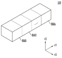
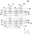
도 3은 도 2의 메모리 셀 어레이의 일 실시 예를 나타낸 도면이다.
도 4는 도 3의 메모리 블록들(BLK1~BLKz) 중 어느 하나의 메모리 블록(BLKa)을 보여주는 회로도이다.
도 5는 도 3의 메모리 블록들(BLK1~BLKz) 중 어느 하나의 메모리 블록(BLKb)의 다른 실시 예를 보여주는 회로도이다.
도 6은 실시 예에 따른 메모리 컨트롤러의 구성 및 동작을 설명하기 위한 도면이다.
도 7은 도 2의 물리 페이지를 설명하기 위한 도면이다.
도 8은 도 2의 물리 페이지의 다른 실시 예를 설명하기 위한 도면이다.
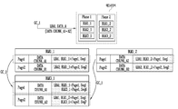
도 9는 실시 예에 따른 히스토리 정보를 저장하는 동작을 설명하기 위한 도면이다.
도 10은 실시 예에 따른 히스토리 정보가 갱신되는 동작을 설명하기 위한 도면이다.
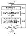
도 11은 실시 예에 따른 메모리 컨트롤러의 동작을 설명하기 위한 순서도이다.
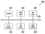
도 12는 도 1의 메모리 컨트롤러의 다른 실시 예를 설명하기 위한 도면이다.
도 13은 본 발명의 실시 예에 따른 저장장치가 적용된 메모리 카드 시스템을 보여주는 블록도이다.
도 14는 본 발명의 실시 예에 따른 저장장치가 적용된 SSD(Solid State Drive) 시스템을 보여주는 블록도이다.
도 15는 본 발명의 실시 예에 따른 저장장치가 적용된 사용자 시스템을 보여주는 블록도이다.
100: 메모리 장치
200: 메모리 컨트롤러
210: 입력 데이터 제어부
220: 시퀀스 정보 생성부
230: 쓰기 동작 제어부
300: 호스트
Claims (25)
- 복수의 페이지들을 포함하는 메모리 장치를 제어하는 메모리 컨트롤러에 있어서,
상기 복수의 페이지들 중 선택된 페이지에 저장할 데이터를 입력 받는 입력 데이터 제어부;
상기 메모리 장치의 동작 상태를 반영하여, 상기 선택된 페이지에 상기 저장할 데이터를 저장하는 프로그램 동작이 수행될 순번을 나타내는 시퀀스 정보를 생성하는 시퀀스 정보 생성부; 및
상기 저장할 데이터를 상기 선택된 페이지의 메인 영역에 저장하고, 상기 선택된 페이지의 물리 주소 및 상기 저장할 데이터에 대응되는 상기 시퀀스 정보를 포함하는 히스토리 정보를 상기 선택된 페이지의 스페어 영역에 저장하도록 상기 메모리 장치를 제어하는 쓰기 동작 제어부;를 포함하는 메모리 컨트롤러. - 제 1항에 있어서, 상기 입력 데이터 제어부는,
상기 메모리 컨트롤러의 외부 호스트로부터 제공된 상기 저장할 데이터를 입력 받는 메모리 컨트롤러. - 제 2항에 있어서, 상기 입력 데이터 제어부는,
상기 호스트로부터 상기 저장할 데이터의 논리 주소를 입력 받는 메모리 컨트롤러. - 제 3항에 있어서, 상기 히스토리 정보는,
상기 논리 주소를 포함하는 메모리 컨트롤러. - 제 1항에 있어서, 상기 입력 데이터 제어부는,
상기 메모리 장치로부터 상기 저장할 데이터를 입력 받는 메모리 컨트롤러. - 제 5항에 있어서, 상기 입력 데이터 제어부는,
상기 복수의 페이지들 중 상기 선택된 페이지와 다른 페이지에 저장된 데이터를 상기 저장할 데이터로 입력 받는 메모리 컨트롤러. - 제 6항에 있어서, 상기 히스토리 정보는,
상기 다른 페이지의 물리주소와 상기 다른 페이지에 저장된 데이터의 프로그램 동작이 수행된 순번을 나타내는 시퀀스 정보를 포함하는 메모리 컨트롤러. - 제 3항에 있어서,
상기 저장할 데이터의 논리 주소와 상기 선택된 페이지의 물리 주소 간의 매핑 정보를 저장하는 매핑 테이블을 더 포함하는 메모리 컨트롤러. - 제 8항에 있어서, 상기 입력 데이터 제어부는,
상기 매핑 테이블을 참조하여, 상기 논리 주소에 대응되는 상기 선택된 페이지의 물리 주소를 상기 쓰기 동작 제어부에 제공하는 메모리 컨트롤러. - 제 1항에 있어서, 상기 시퀀스 정보 생성부는,
상기 메모리 장치에 의해 수행된 프로그램 동작들의 총 횟수에 따라 상기 시퀀스 정보를 결정하는 메모리 컨트롤러. - 제 10항에 있어서, 상기 시퀀스 정보 생성부는,
상기 프로그램 동작들의 횟수를 카운트하는 카운트 회로를 포함하는 메모리 컨트롤러. - 제 11항에 있어서, 상기 쓰기 동작 제어부는,
상기 프로그램 동작이 수행됨을 나타내는 프로그램 동작 수행 정보를 생성하는 메모리 컨트롤러. - 제 12항에 있어서, 상기 카운트 회로는,
상기 프로그램 동작 수행 정보를 기초로 상기 프로그램 동작들의 횟수를 카운트하는 메모리 컨트롤러. - 제 1항에 있어서, 상기 선택된 페이지의 스페어 영역은,
미리 설정된 커맨드에 의해 액세스되는 메모리 컨트롤러. - 제 1항에 있어서, 상기 입력 데이터 제어부는,
상기 저장할 데이터를 페이지 단위로 저장되는 적어도 하나의 데이터 청크로 구분하는 메모리 컨트롤러. - 제 15항에 있어서, 상기 시퀀스 정보 생성부는,
상기 메모리 장치에 의해 수행된 프로그램 동작들의 총 횟수에 따라 결정되고, 상기 선택된 페이지에 상기 적어도 하나의 데이터 청크 중 어느 하나의 데이터 청크를 저장하는 프로그램 동작이 수행될 순번을 나타내는 청크 시퀀스 정보를 생성하는 메모리 컨트롤러. - 제 16항에 있어서, 상기 쓰기 동작 제어부는,
상기 어느 하나의 데이터 청크를 상기 선택된 페이지의 메인 영역에 저장하고, 상기 선택된 페이지의 물리 주소 및 상기 어느 하나의 데이터 청크에 대응되는 상기 청크 시퀀스 정보를 상기 선택된 페이지의 스페어 영역에 저장하도록 상기 메모리 장치를 제어하는 메모리 컨트롤러. - 복수의 페이지들을 포함하는 메모리 장치를 제어하는 메모리 컨트롤러의 동작 방법에 있어서,
상기 복수의 페이지들 중 선택된 페이지에 저장할 데이터를 입력 받는 단계;
상기 메모리 장치에 의해 수행된 프로그램 동작들의 총 횟수를 카운트하는 단계;
상기 총 횟수를 기초로, 상기 선택된 페이지에 상기 저장할 데이터를 저장하는 프로그램 동작이 수행될 순번을 결정하고, 상기 순번을 나타내는 시퀀스 정보를 생성하는 단계; 및
상기 저장할 데이터를 상기 선택된 페이지의 메인 영역에 저장하고, 상기 선택된 페이지의 물리 주소 및 상기 저장할 데이터에 대응되는 상기 시퀀스 정보를 포함하는 히스토리 정보를 상기 선택된 페이지의 스페어 영역에 저장하는 프로그램 커맨드를 상기 메모리 장치를 제공하는 단계를 포함하는 메모리 컨트롤러의 동작 방법. - 제 18항에 있어서, 상기 저장할 데이터를 입력 받는 단계는,
상기 메모리 컨트롤러의 외부 호스트로부터 상기 저장할 데이터를 입력 받거나 상기 메모리 장치로부터 상기 저장할 데이터를 입력 받는 메모리 컨트롤러의 동작 방법. - 제 19항에 있어서,
상기 메모리 장치로부터 입력 받은 상기 저장할 데이터는,
상기 복수의 페이지들 중 상기 선택된 페이지와 다른 페이지에 저장된 데이터이고,
상기 히스토리 정보는,
상기 다른 페이지의 물리주소와 상기 다른 페이지에 저장된 데이터의 프로그램 동작이 수행된 순번을 나타내는 시퀀스 정보를 포함하는 메모리 컨트롤러의 동작 방법. - 복수의 페이지들을 포함하고, 상기 복수의 페이지들 중 선택된 페이지에 데이터를 저장하는 프로그램 동작을 수행하는 메모리 장치; 및
호스트 또는 상기 메모리 장치로부터 상기 데이터를 입력 받고, 상기 메모리 장치의 동작 상태를 반영하여, 상기 프로그램 동작이 수행될 순번을 나타내는 시퀀스 정보를 생성하고,
상기 데이터를 상기 선택된 페이지의 메인 영역에 저장하고, 상기 선택된 페이지의 물리 주소 및 상기 데이터에 대응되는 상기 시퀀스 정보를 포함하는 히스토리 정보를 상기 선택된 페이지의 스페어 영역에 저장하는 상기 프로그램 동작을 지시하는 프로그램 커맨드를 상기 메모리 장치를 제공하는 메모리 컨트롤러를 포함하는 저장 장치. - 제 21항에 있어서, 상기 메모리 컨트롤러는,
상기 메모리 장치에 의해 수행된 프로그램 동작들의 총 횟수에 따라 상기 시퀀스 정보를 결정하는 저장 장치. - 제 22항에 있어서, 상기 메모리 컨트롤러는,
상기 메모리 장치로부터 상기 데이터를 입력 받고,
상기 데이터는,
상기 복수의 페이지들 중 상기 선택된 페이지와 다른 페이지에 저장된 데이터가 리드된 데이터인 저장 장치. - 제 23항에 있어서, 상기 히스토리 정보는,
상기 다른 페이지의 물리주소와 상기 다른 페이지에 저장된 데이터의 프로그램 동작이 수행된 순번을 나타내는 시퀀스 정보를 포함하는 저장 장치. - 제 21항에 있어서, 상기 메모리 컨트롤러는,
상기 호스트로부터 수신한 미리 설정된 커맨드에 응답하여 상기 선택된 페이지의 스페어 영역을 액세스하고,
상기 미리 설정된 커맨드는,
상기 메모리 장치를 테스트하는데 사용되는 커맨드 및 상기 메모리 장치를 분석하기 위한 데이터를 요청하는 커맨드를 포함하는 저장 장치.
Priority Applications (4)
| Application Number | Priority Date | Filing Date | Title |
|---|---|---|---|
| KR1020190006417A KR20200089547A (ko) | 2019-01-17 | 2019-01-17 | 저장 장치 및 그 동작 방법 |
| US16/584,482 US11194732B2 (en) | 2019-01-17 | 2019-09-26 | Storage device and method of operating the same |
| CN201910982396.7A CN111445939B (zh) | 2019-01-17 | 2019-10-16 | 存储装置及其操作方法 |
| KR1020240098843A KR102729143B1 (ko) | 2019-01-17 | 2024-07-25 | 저장 장치 및 그 동작 방법 |
Applications Claiming Priority (1)
| Application Number | Priority Date | Filing Date | Title |
|---|---|---|---|
| KR1020190006417A KR20200089547A (ko) | 2019-01-17 | 2019-01-17 | 저장 장치 및 그 동작 방법 |
Related Child Applications (1)
| Application Number | Title | Priority Date | Filing Date |
|---|---|---|---|
| KR1020240098843A Division KR102729143B1 (ko) | 2019-01-17 | 2024-07-25 | 저장 장치 및 그 동작 방법 |
Publications (1)
| Publication Number | Publication Date |
|---|---|
| KR20200089547A true KR20200089547A (ko) | 2020-07-27 |
Family
ID=71610254
Family Applications (2)
| Application Number | Title | Priority Date | Filing Date |
|---|---|---|---|
| KR1020190006417A Ceased KR20200089547A (ko) | 2019-01-17 | 2019-01-17 | 저장 장치 및 그 동작 방법 |
| KR1020240098843A Active KR102729143B1 (ko) | 2019-01-17 | 2024-07-25 | 저장 장치 및 그 동작 방법 |
Family Applications After (1)
| Application Number | Title | Priority Date | Filing Date |
|---|---|---|---|
| KR1020240098843A Active KR102729143B1 (ko) | 2019-01-17 | 2024-07-25 | 저장 장치 및 그 동작 방법 |
Country Status (3)
| Country | Link |
|---|---|
| US (1) | US11194732B2 (ko) |
| KR (2) | KR20200089547A (ko) |
| CN (1) | CN111445939B (ko) |
Families Citing this family (4)
| Publication number | Priority date | Publication date | Assignee | Title |
|---|---|---|---|---|
| WO2019031295A1 (ja) * | 2017-08-08 | 2019-02-14 | パナソニックIpマネジメント株式会社 | カード装置、ホスト装置および通信方法 |
| KR102849331B1 (ko) * | 2021-06-25 | 2025-08-25 | 에스케이하이닉스 주식회사 | 메모리 장치 및 메모리 장치의 동작 방법 |
| CN115129621B (zh) * | 2022-09-01 | 2022-12-02 | 珠海星云智联科技有限公司 | 一种内存管理方法、设备、介质及内存管理模块 |
| KR20250153460A (ko) * | 2024-04-18 | 2025-10-27 | 에스케이하이닉스 주식회사 | 저전력 모드에서 데이터를 페이지 버퍼에 백업하는 스토리지 장치 및 그 동작 방법 |
Family Cites Families (22)
| Publication number | Priority date | Publication date | Assignee | Title |
|---|---|---|---|---|
| CN100442393C (zh) | 1999-10-21 | 2008-12-10 | 松下电器产业株式会社 | 半导体存储卡的访问装置、初始化方法和半导体存储卡 |
| KR100528482B1 (ko) * | 2003-12-31 | 2005-11-15 | 삼성전자주식회사 | 데이타를 섹터 단위로 랜덤하게 입출력할 수 있는 플래시메모리 시스템 |
| JP4967680B2 (ja) * | 2007-01-23 | 2012-07-04 | ソニー株式会社 | 記憶装置およびコンピュータシステム、並びに記憶装置の管理方法 |
| KR100882740B1 (ko) | 2007-02-22 | 2009-02-09 | 삼성전자주식회사 | 맵 히스토리 기반의 불휘발성 메모리의 매핑 방법 및 저장장치 |
| US8438325B2 (en) * | 2008-10-09 | 2013-05-07 | Cadence Design Systems, Inc. | Method and apparatus for improving small write performance in a non-volatile memory |
| JP5402044B2 (ja) | 2009-02-09 | 2014-01-29 | 富士ゼロックス株式会社 | 保守制御装置、保守制御システム及び保守制御プログラム |
| US8219776B2 (en) * | 2009-09-23 | 2012-07-10 | Lsi Corporation | Logical-to-physical address translation for solid state disks |
| US8495338B2 (en) | 2010-12-03 | 2013-07-23 | Micron Technology, Inc. | Transaction log recovery |
| KR20120137867A (ko) * | 2011-06-13 | 2012-12-24 | 삼성전자주식회사 | 상변화 물질을 포함하는 비휘발성 메모리 장치 및 이의 제조 방법 |
| US9164676B2 (en) * | 2011-11-30 | 2015-10-20 | International Business Machines Corporation | Storing multi-stream non-linear access patterns in a flash based file-system |
| KR102053953B1 (ko) * | 2013-02-04 | 2019-12-11 | 삼성전자주식회사 | 불휘발성 메모리 장치를 포함하는 메모리 시스템 및 그것의 프로그램 방법 |
| KR102128406B1 (ko) * | 2014-09-26 | 2020-07-10 | 삼성전자주식회사 | 스토리지 장치 및 스토리지 장치의 동작 방법 |
| KR102403202B1 (ko) * | 2015-03-13 | 2022-05-30 | 삼성전자주식회사 | 메타 데이터 관리자를 포함하는 메모리 시스템 및 동작 방법 |
| US9727244B2 (en) * | 2015-10-05 | 2017-08-08 | International Business Machines Corporation | Expanding effective storage capacity of a data storage system while providing support for address mapping recovery |
| TWI604308B (zh) * | 2015-11-18 | 2017-11-01 | 慧榮科技股份有限公司 | 資料儲存裝置及其資料維護方法 |
| KR102438988B1 (ko) * | 2016-04-07 | 2022-09-02 | 삼성전자주식회사 | 랜덤화 연산을 수행하는 불휘발성 메모리 장치 |
| US9841921B2 (en) * | 2016-04-27 | 2017-12-12 | Pure Storage, Inc. | Migrating data in a storage array that includes a plurality of storage devices |
| KR102580123B1 (ko) * | 2016-05-03 | 2023-09-20 | 삼성전자주식회사 | Raid 스토리지 장치 및 그것의 관리 방법 |
| KR102730871B1 (ko) | 2016-09-19 | 2024-11-19 | 에스케이하이닉스 주식회사 | 메모리 시스템 및 메모리 시스템의 동작 방법 |
| KR20190000663A (ko) * | 2017-06-23 | 2019-01-03 | 에스케이하이닉스 주식회사 | 메모리 장치 및 그 동작 방법 |
| KR102645740B1 (ko) * | 2018-10-30 | 2024-03-11 | 에스케이하이닉스 주식회사 | 저장 장치 및 그 동작 방법 |
| KR102763939B1 (ko) * | 2019-12-24 | 2025-02-07 | 에스케이하이닉스 주식회사 | 스토리지 장치 및 그 동작 방법 |
-
2019
- 2019-01-17 KR KR1020190006417A patent/KR20200089547A/ko not_active Ceased
- 2019-09-26 US US16/584,482 patent/US11194732B2/en active Active
- 2019-10-16 CN CN201910982396.7A patent/CN111445939B/zh active Active
-
2024
- 2024-07-25 KR KR1020240098843A patent/KR102729143B1/ko active Active
Also Published As
| Publication number | Publication date |
|---|---|
| KR102729143B1 (ko) | 2024-11-13 |
| CN111445939A (zh) | 2020-07-24 |
| CN111445939B (zh) | 2023-07-25 |
| US11194732B2 (en) | 2021-12-07 |
| KR20240118051A (ko) | 2024-08-02 |
| US20200233812A1 (en) | 2020-07-23 |
Similar Documents
| Publication | Publication Date | Title |
|---|---|---|
| KR102761978B1 (ko) | 저장 장치 및 그 동작 방법 | |
| KR102535104B1 (ko) | 저장 장치 및 그 동작 방법 | |
| KR102391499B1 (ko) | 저장 장치 및 그 동작 방법 | |
| KR102736266B1 (ko) | 저장 장치 및 그 동작 방법 | |
| KR102698994B1 (ko) | 저장 장치 및 그 동작 방법 | |
| KR102717014B1 (ko) | 저장 장치 및 그 동작 방법 | |
| KR102675307B1 (ko) | 저장 장치 및 그 동작 방법 | |
| KR20200088713A (ko) | 메모리 컨트롤러 및 그 동작 방법 | |
| KR102724610B1 (ko) | 저장 장치 및 그 동작 방법 | |
| KR20200056880A (ko) | 저장 장치 및 그 동작 방법 | |
| KR102724063B1 (ko) | 저장 장치 및 그 동작 방법 | |
| KR102729143B1 (ko) | 저장 장치 및 그 동작 방법 | |
| KR20200091199A (ko) | 저장 장치, 저장 장치를 포함하는 컴퓨팅 시스템 및 그 동작 방법 | |
| KR20200088709A (ko) | 저장 장치 및 그 동작 방법 | |
| KR20190100782A (ko) | 스토리지 장치 및 그 동작 방법 | |
| KR20200137313A (ko) | 메모리 장치, 메모리 컨트롤러 및 이들을 포함하는 저장 장치 | |
| KR20210090439A (ko) | 메모리 컨트롤러 및 그 동작 방법 | |
| KR20220048377A (ko) | 저장 장치 및 그 동작 방법 | |
| KR102743801B1 (ko) | 저장 장치 및 그 동작 방법 | |
| KR102556276B1 (ko) | 저장 장치 및 그 동작 방법 | |
| KR20200066893A (ko) | 메모리 컨트롤러 및 그 동작 방법 | |
| KR20230012334A (ko) | 메모리 장치 및 그 동작 방법 | |
| KR20220046308A (ko) | 저장 장치 및 그 동작 방법 | |
| KR102456175B1 (ko) | 저장 장치 및 그 동작 방법 | |
| KR20210054399A (ko) | 저장 장치 및 그 동작 방법 |
Legal Events
| Date | Code | Title | Description |
|---|---|---|---|
| PA0109 | Patent application |
Patent event code: PA01091R01D Comment text: Patent Application Patent event date: 20190117 |
|
| PG1501 | Laying open of application | ||
| A201 | Request for examination | ||
| PA0201 | Request for examination |
Patent event code: PA02012R01D Patent event date: 20211209 Comment text: Request for Examination of Application Patent event code: PA02011R01I Patent event date: 20190117 Comment text: Patent Application |
|
| E902 | Notification of reason for refusal | ||
| PE0902 | Notice of grounds for rejection |
Comment text: Notification of reason for refusal Patent event date: 20230925 Patent event code: PE09021S01D |
|
| E601 | Decision to refuse application | ||
| PE0601 | Decision on rejection of patent |
Patent event date: 20240116 Comment text: Decision to Refuse Application Patent event code: PE06012S01D Patent event date: 20230925 Comment text: Notification of reason for refusal Patent event code: PE06011S01I |
|
| E601 | Decision to refuse application | ||
| E801 | Decision on dismissal of amendment | ||
| PE0601 | Decision on rejection of patent |
Patent event date: 20240424 Comment text: Decision to Refuse Application Patent event code: PE06012S01D Patent event date: 20230925 Comment text: Notification of reason for refusal Patent event code: PE06011S01I |
|
| PE0801 | Dismissal of amendment |
Patent event code: PE08012E01D Comment text: Decision on Dismissal of Amendment Patent event date: 20240424 Patent event code: PE08011R01I Comment text: Amendment to Specification, etc. Patent event date: 20240417 Patent event code: PE08011R01I Comment text: Amendment to Specification, etc. Patent event date: 20231123 Patent event code: PE08011R01I Comment text: Amendment to Specification, etc. Patent event date: 20211209 |