KR20200089761A - 자동-참조 메모리 셀 판독 기법 - Google Patents
자동-참조 메모리 셀 판독 기법 Download PDFInfo
- Publication number
- KR20200089761A KR20200089761A KR1020207020354A KR20207020354A KR20200089761A KR 20200089761 A KR20200089761 A KR 20200089761A KR 1020207020354 A KR1020207020354 A KR 1020207020354A KR 20207020354 A KR20207020354 A KR 20207020354A KR 20200089761 A KR20200089761 A KR 20200089761A
- Authority
- KR
- South Korea
- Prior art keywords
- memory
- bit
- memory cells
- bits
- memory cell
- Prior art date
- Legal status (The legal status is an assumption and is not a legal conclusion. Google has not performed a legal analysis and makes no representation as to the accuracy of the status listed.)
- Granted
Links
Images






Classifications
-
- G—PHYSICS
- G11—INFORMATION STORAGE
- G11C—STATIC STORES
- G11C11/00—Digital stores characterised by the use of particular electric or magnetic storage elements; Storage elements therefor
- G11C11/56—Digital stores characterised by the use of particular electric or magnetic storage elements; Storage elements therefor using storage elements with more than two stable states represented by steps, e.g. of voltage, current, phase, frequency
- G11C11/5621—Digital stores characterised by the use of particular electric or magnetic storage elements; Storage elements therefor using storage elements with more than two stable states represented by steps, e.g. of voltage, current, phase, frequency using charge storage in a floating gate
- G11C11/5642—Sensing or reading circuits; Data output circuits
-
- G—PHYSICS
- G11—INFORMATION STORAGE
- G11B—INFORMATION STORAGE BASED ON RELATIVE MOVEMENT BETWEEN RECORD CARRIER AND TRANSDUCER
- G11B20/00—Signal processing not specific to the method of recording or reproducing; Circuits therefor
- G11B20/10—Digital recording or reproducing
-
- G—PHYSICS
- G11—INFORMATION STORAGE
- G11C—STATIC STORES
- G11C11/00—Digital stores characterised by the use of particular electric or magnetic storage elements; Storage elements therefor
- G11C11/56—Digital stores characterised by the use of particular electric or magnetic storage elements; Storage elements therefor using storage elements with more than two stable states represented by steps, e.g. of voltage, current, phase, frequency
- G11C11/5678—Digital stores characterised by the use of particular electric or magnetic storage elements; Storage elements therefor using storage elements with more than two stable states represented by steps, e.g. of voltage, current, phase, frequency using amorphous/crystalline phase transition storage elements
-
- G—PHYSICS
- G11—INFORMATION STORAGE
- G11C—STATIC STORES
- G11C13/00—Digital stores characterised by the use of storage elements not covered by groups G11C11/00, G11C23/00, or G11C25/00
- G11C13/0002—Digital stores characterised by the use of storage elements not covered by groups G11C11/00, G11C23/00, or G11C25/00 using resistive RAM [RRAM] elements
- G11C13/0004—Digital stores characterised by the use of storage elements not covered by groups G11C11/00, G11C23/00, or G11C25/00 using resistive RAM [RRAM] elements comprising amorphous/crystalline phase transition cells
-
- G—PHYSICS
- G11—INFORMATION STORAGE
- G11C—STATIC STORES
- G11C13/00—Digital stores characterised by the use of storage elements not covered by groups G11C11/00, G11C23/00, or G11C25/00
- G11C13/0002—Digital stores characterised by the use of storage elements not covered by groups G11C11/00, G11C23/00, or G11C25/00 using resistive RAM [RRAM] elements
- G11C13/0021—Auxiliary circuits
- G11C13/003—Cell access
-
- G—PHYSICS
- G11—INFORMATION STORAGE
- G11C—STATIC STORES
- G11C13/00—Digital stores characterised by the use of storage elements not covered by groups G11C11/00, G11C23/00, or G11C25/00
- G11C13/0002—Digital stores characterised by the use of storage elements not covered by groups G11C11/00, G11C23/00, or G11C25/00 using resistive RAM [RRAM] elements
- G11C13/0021—Auxiliary circuits
- G11C13/0033—Disturbance prevention or evaluation; Refreshing of disturbed memory data
-
- G—PHYSICS
- G11—INFORMATION STORAGE
- G11C—STATIC STORES
- G11C13/00—Digital stores characterised by the use of storage elements not covered by groups G11C11/00, G11C23/00, or G11C25/00
- G11C13/0002—Digital stores characterised by the use of storage elements not covered by groups G11C11/00, G11C23/00, or G11C25/00 using resistive RAM [RRAM] elements
- G11C13/0021—Auxiliary circuits
- G11C13/004—Reading or sensing circuits or methods
-
- G—PHYSICS
- G11—INFORMATION STORAGE
- G11C—STATIC STORES
- G11C13/00—Digital stores characterised by the use of storage elements not covered by groups G11C11/00, G11C23/00, or G11C25/00
- G11C13/02—Digital stores characterised by the use of storage elements not covered by groups G11C11/00, G11C23/00, or G11C25/00 using elements whose operation depends upon chemical change
-
- G—PHYSICS
- G11—INFORMATION STORAGE
- G11C—STATIC STORES
- G11C16/00—Erasable programmable read-only memories
- G11C16/02—Erasable programmable read-only memories electrically programmable
- G11C16/06—Auxiliary circuits, e.g. for writing into memory
- G11C16/08—Address circuits; Decoders; Word-line control circuits
-
- G—PHYSICS
- G11—INFORMATION STORAGE
- G11C—STATIC STORES
- G11C16/00—Erasable programmable read-only memories
- G11C16/02—Erasable programmable read-only memories electrically programmable
- G11C16/06—Auxiliary circuits, e.g. for writing into memory
- G11C16/10—Programming or data input circuits
-
- G—PHYSICS
- G11—INFORMATION STORAGE
- G11C—STATIC STORES
- G11C16/00—Erasable programmable read-only memories
- G11C16/02—Erasable programmable read-only memories electrically programmable
- G11C16/06—Auxiliary circuits, e.g. for writing into memory
- G11C16/30—Power supply circuits
-
- G—PHYSICS
- G11—INFORMATION STORAGE
- G11C—STATIC STORES
- G11C16/00—Erasable programmable read-only memories
- G11C16/02—Erasable programmable read-only memories electrically programmable
- G11C16/06—Auxiliary circuits, e.g. for writing into memory
- G11C16/32—Timing circuits
-
- G—PHYSICS
- G11—INFORMATION STORAGE
- G11C—STATIC STORES
- G11C7/00—Arrangements for writing information into, or reading information out from, a digital store
- G11C7/04—Arrangements for writing information into, or reading information out from, a digital store with means for avoiding disturbances due to temperature effects
-
- G—PHYSICS
- G11—INFORMATION STORAGE
- G11C—STATIC STORES
- G11C7/00—Arrangements for writing information into, or reading information out from, a digital store
- G11C7/10—Input/output [I/O] data interface arrangements, e.g. I/O data control circuits, I/O data buffers
- G11C7/1006—Data managing, e.g. manipulating data before writing or reading out, data bus switches or control circuits therefor
-
- G—PHYSICS
- G11—INFORMATION STORAGE
- G11C—STATIC STORES
- G11C7/00—Arrangements for writing information into, or reading information out from, a digital store
- G11C7/14—Dummy cell management; Sense reference voltage generators
-
- G—PHYSICS
- G11—INFORMATION STORAGE
- G11C—STATIC STORES
- G11C8/00—Arrangements for selecting an address in a digital store
- G11C8/14—Word line organisation; Word line lay-out
-
- G—PHYSICS
- G11—INFORMATION STORAGE
- G11C—STATIC STORES
- G11C13/00—Digital stores characterised by the use of storage elements not covered by groups G11C11/00, G11C23/00, or G11C25/00
- G11C13/0002—Digital stores characterised by the use of storage elements not covered by groups G11C11/00, G11C23/00, or G11C25/00 using resistive RAM [RRAM] elements
- G11C13/0021—Auxiliary circuits
- G11C13/004—Reading or sensing circuits or methods
- G11C2013/0054—Read is performed on a reference element, e.g. cell, and the reference sensed value is used to compare the sensed value of the selected cell
-
- G—PHYSICS
- G11—INFORMATION STORAGE
- G11C—STATIC STORES
- G11C2211/00—Indexing scheme relating to digital stores characterized by the use of particular electric or magnetic storage elements; Storage elements therefor
- G11C2211/56—Indexing scheme relating to G11C11/56 and sub-groups for features not covered by these groups
- G11C2211/563—Multilevel memory reading aspects
- G11C2211/5634—Reference cells
-
- G—PHYSICS
- G11—INFORMATION STORAGE
- G11C—STATIC STORES
- G11C2213/00—Indexing scheme relating to G11C13/00 for features not covered by this group
- G11C2213/70—Resistive array aspects
- G11C2213/71—Three dimensional array
-
- G—PHYSICS
- G11—INFORMATION STORAGE
- G11C—STATIC STORES
- G11C2213/00—Indexing scheme relating to G11C13/00 for features not covered by this group
- G11C2213/70—Resistive array aspects
- G11C2213/76—Array using an access device for each cell which being not a transistor and not a diode
Landscapes
- Engineering & Computer Science (AREA)
- Chemical & Material Sciences (AREA)
- Crystallography & Structural Chemistry (AREA)
- Computer Hardware Design (AREA)
- Microelectronics & Electronic Packaging (AREA)
- Semiconductor Memories (AREA)
- Read Only Memory (AREA)
- Signal Processing (AREA)
- Memory System (AREA)
Abstract
Description
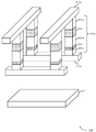
도 2는 본 발명의 실시형태에 따른 자동-참조 메모리 셀 판독 기법을 지원하는 3D 메모리 어레이의 일 실시예를 도시하는 도면;
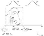
도 3은 본 발명의 실시형태에 따른 자동-참조 메모리 셀 판독 기법을 지원하는 임계 전압 분포의 실시예를 도시하는 도면;
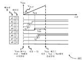
도 4a 및 도 4b는 본 발명의 실시형태에 따른 자동-참조 메모리 셀 판독 기법을 지원하는 기법을 도시하는 도면;
도 5a 및 도 5b는 본 발명의 실시형태에 따른 자동-참조 메모리 셀 판독 기법을 지원하는 사용자 데이터 패턴 및 회로도의 실시예를 도시하는 도면;
도 6은 본 발명의 실시형태에 따른 자동-참조 메모리 셀 판독 기법을 도시하는 도면;
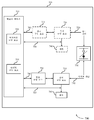
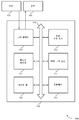
도 7 및 도 8은 본 발명의 실시형태에 따른 자동-참조 메모리 셀 판독 기법을 지원하는 디바이스의 블록도를 도시하는 도면;
도 9는 본 발명의 실시형태에 따른 자동-참조 메모리 셀 판독 기법을 지원하는 메모리 어레이를 포함하는 시스템의 블록도를 도시하는 도면; 및
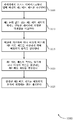
도 10 내지 도 13은 본 발명의 실시형태에 따른 자동-참조 메모리 셀 판독 기법을 위한 방법을 도시하는 도면.


Claims (25)
- 방법으로서,
제어기에서, 호스트 디바이스로부터 입력 벡터의 제1 비트 세트를 수신하는 단계;
제1 논리값을 갖는 상기 제1 비트 세트의 적어도 일부를 상기 제어기에 저장된 임계값과 비교하는 단계;
상기 비교에 적어도 부분적으로 기초하여 하나 이상의 비트와 상기 제1 비트 세트를 저장하기 위해 메모리의 블록을 할당하는 단계;
상기 제1 비트 세트의 적어도 일부와 상기 하나 이상의 비트를 포함하는 제2 비트 세트를 생성하는 단계; 및
생성된 제2 비트 세트를 상기 메모리의 블록에 저장하는 것을 개시하는 단계를 포함하는 방법. - 제1항에 있어서,
상기 임계값과 연관된 인자에 적어도 부분적으로 기초하여 상기 제1 비트 세트를 하나 이상의 비트 세그먼트로 분할하는 단계;
상기 하나 이상의 비트 세그먼트 중 적어도 하나의 비트 세그먼트를 선택하는 단계; 및
선택된 적어도 하나의 비트 세그먼트의 비트 세트의 논리 상태를 반전시키는 단계를 더 포함하고, 상기 하나 이상의 비트의 값은 상기 비트 세트의 반전된 논리 상태에 적어도 부분적으로 기초하는, 방법. - 제2항에 있어서,
상기 인자에 적어도 부분적으로 기초하여 상기 하나 이상의 비트 세그먼트의 비트 세그먼트의 수를 결정하는 단계를 더 포함하되, 상기 하나 이상의 비트의 수는 상기 비트 세그먼트의 수에 대응하는, 방법. - 제1항에 있어서, 상기 제1 비트 세트의 적어도 일부를 비교하는 단계는,
제1 논리 상태를 갖는 상기 입력 벡터의 비트의 백분율을 식별하는 단계; 및
상기 백분율을 백분율 범위와 비교하는 단계를 포함하고, 상기 백분율 범위는 상기 임계값과 연관된 인자에 적어도 부분적으로 기초하는, 방법. - 제1항에 있어서, 상기 제1 비트 세트의 적어도 일부를 비교하는 단계는,
상기 제1 비트 세트의 수가 상기 임계값을 충족시키지 않는다고 결정하는 단계; 및
상기 제1 비트 세트의 수가 상기 임계값을 충족시키지 않는다는 결정에 적어도 부분적으로 기초하여 상기 제1 비트 세트의 각각의 논리 상태를 반전시키는 단계를 포함하는, 방법. - 제5항에 있어서,
상기 제1 비트 세트의 수가 상기 제1 비트 세트의 각각의 논리 상태를 반전시키는 것에 적어도 부분적으로 기초하여 상기 임계값을 충족시키지 않는다고 결정하는 단계;
상기 제1 비트 세트의 수가 상기 반전 후 상기 임계값을 충족시키지 않는다는 결정에 기초하여 상기 제1 비트 세트의 원래의 논리 상태를 복원하는 단계; 및
상기 제1 논리값을 갖는 상기 제1 비트 세트의 다른 부분을 상기 제어기에 저장된 상기 임계값과 비교하는 단계를 더 포함하는, 방법. - 제1항에 있어서, 상기 제1 비트 세트의 적어도 일부를 비교하는 단계는,
상기 입력 벡터의 패턴 가중치를 상기 임계값과 연관된 인자에 적어도 부분적으로 기초한 범위와 비교하는 단계를 포함하는, 방법. - 제1항에 있어서,
제1 논리 상태를 갖는 비트의 수에 적어도 부분적으로 기초하여 상기 입력 벡터의 패턴 가중치를 결정하는 단계를 더 포함하되, 상기 제1 논리 상태는 메모리 셀의 제1 세트의 임계 전압과 연관되고, 상기 제1 세트의 임계 전압은 상기 제1 논리 상태와는 다른 제2 논리 상태와 연관된 제2 세트의 임계 전압보다 더 작은, 방법. - 방법으로서,
메모리 어레이의 메모리 셀의 그룹을 활성화시키기 위해 활성화 전압을 상기 메모리 어레이에 인가하는 단계;
상기 활성화 전압을 인가하는 것에 적어도 부분적으로 기초하여 제1 시간에 제1 세트의 메모리 셀이 활성화되었다고 결정하는 단계;
상기 제1 시간 후 지속 기간 동안 상기 활성화 전압의 인가를 유지하는 단계; 및
상기 지속 기간의 종료 후, 상기 제1 세트의 메모리 셀을 포함하는 제2 세트의 메모리 셀의 논리 상태를 판독하는 단계를 포함하는 방법. - 제9항에 있어서,
상기 제2 세트의 메모리 셀이 제1 논리 상태에 대응하는 것이라고 결정하는 단계를 더 포함하는, 방법. - 제9항에 있어서,
상기 제1 세트의 메모리 셀이 활성화되었다는 결정은 상기 메모리 셀의 그룹의 서브세트의 중앙(median) 임계 전압값에 적어도 부분적으로 기초하고, 상기 메모리 셀의 서브세트의 임계 전압은 상기 그룹의 나머지 메모리 셀의 임계 전압보다 더 작은, 방법. - 제9항에 있어서,
상기 지속 기간은 추가 메모리 셀을 활성화시키는 것에 적어도 부분적으로 기초하여 결정되고, 상기 제2 세트의 메모리 셀은 상기 제1 세트의 메모리 셀 및 추가 메모리 셀을 포함하는, 방법. - 제9항에 있어서,
상기 활성화 전압은 메모리 셀의 세트의 최소 임계 전압보다 더 작은 초기값을 갖는, 방법. - 제9항에 있어서,
상기 활성화 전압은, 메모리 셀의 세트의 최소 임계 전압보다 더 크고 상기 메모리 셀의 세트의 중앙 임계 전압보다 더 작은 초기값을 갖는, 방법. - 제9항에 있어서,
상기 활성화 전압은 시간에 따라 일정한 증가율을 갖는, 방법. - 제9항에 있어서,
제3 세트의 메모리 셀이 제1 논리 상태와는 다른 제2 논리 상태에 대응하는 것이라고 결정하는 단계를 더 포함하되, 상기 제3 세트의 메모리 셀은 상기 지속 기간의 종료 후에 비활성화되는, 방법. - 전자 메모리 장치로서,
메모리 매체; 및
상기 메모리 매체와 결합된 제어기를 포함하되, 상기 제어기는,
호스트 디바이스로부터 입력 벡터의 제1 비트 세트를 수신하고;
제1 논리값을 갖는 상기 제1 비트 세트의 적어도 일부를 상기 제어기에 저장된 임계값과 비교하고;
상기 비교에 적어도 부분적으로 기초하여 하나 이상의 비트와 상기 제1 비트 세트를 저장하기 위해 상기 메모리 매체의 메모리의 블록을 할당하고;
상기 제1 비트 세트의 적어도 일부와 상기 하나 이상의 비트를 포함하는 제2 비트 세트를 생성하고;
생성된 제2 비트 세트를 상기 메모리의 블록에 저장하는 것을 개시하도록 동작 가능한, 전자 메모리 장치. - 제17항에 있어서, 상기 제어기는,
상기 임계값과 연관된 인자에 적어도 부분적으로 기초하여 상기 제1 비트 세트를 하나 이상의 비트 세그먼트로 분할하고;
상기 하나 이상의 비트 세그먼트 중 적어도 하나의 비트 세그먼트를 선택하고;
선택된 적어도 하나의 비트 세그먼트의 비트 세트의 논리 상태를 반전시키도록 더 동작 가능하고, 상기 하나 이상의 비트의 값은 상기 비트 세트의 반전된 논리 상태에 적어도 부분적으로 기초하는, 전자 메모리 장치. - 제17항에 있어서, 상기 제어기는,
제1 논리 상태를 갖는 상기 입력 벡터의 비트의 백분율을 식별하고;
상기 백분율을 백분율 범위와 비교하도록 더 동작 가능하고, 상기 백분율 범위는 상기 임계값과 연관된 인자에 적어도 부분적으로 기초하는, 전자 메모리 장치. - 제17항에 있어서, 상기 제어기는,
상기 제1 비트 세트의 수가 상기 임계값을 충족시키지 않는다고 결정하고;
상기 제1 비트 세트의 수가 상기 임계값을 충족시키지 않는다는 결정에 적어도 부분적으로 기초하여 상기 제1 비트 세트의 각각의 논리 상태를 반전시키도록 더 동작 가능한, 전자 메모리 장치. - 제17항에 있어서, 상기 제어기는,
상기 입력 벡터의 패턴 가중치를 범위와 비교하도록 더 동작 가능하고, 상기 범위는 상기 임계값과 연관된 인자에 적어도 부분적으로 기초하는, 전자 메모리 장치. - 제17항에 있어서,
상기 메모리 매체는 상 변화 메모리 셀의 3차원 교차점 어레이를 포함하는, 전자 메모리 장치. - 전자 메모리 장치로서,
메모리 어레이; 및
상기 메모리 어레이와 전자 통신하는 제어기를 포함하되, 상기 제어기는,
상기 메모리 어레이의 메모리 셀의 그룹을 활성화시키기 위해 상기 메모리 어레이에 활성화 전압을 인가하고;
상기 활성화 전압을 인가하는 것에 적어도 부분적으로 기초하여 제1 시간에 제1 세트의 메모리 셀이 활성화되었다고 결정하고;
상기 제1 시간 후 지속 기간 동안 상기 활성화 전압의 인가를 유지하고;
상기 지속 기간의 종료 후에, 상기 제1 세트의 메모리 셀을 포함하는 제2 세트의 메모리 셀의 논리 상태를 판독하도록 동작 가능한, 전자 메모리 장치. - 제23항에 있어서, 상기 제어기는,
상기 제2 세트의 메모리 셀이 제1 논리 상태에 대응하는 것이라고 결정하도록 더 동작 가능한, 전자 메모리 장치. - 제23항에 있어서, 상기 제어기는,
상기 제1 세트의 메모리 셀이 상기 메모리 셀의 그룹의 서브세트의 중앙 임계 전압값에 적어도 부분적으로 기초하여 활성화되었다고 결정하도록 더 동작 가능하고, 상기 메모리 셀의 서브세트의 임계 전압은 상기 그룹의 나머지 메모리 셀의 임계 전압보다 더 작은, 전자 메모리 장치.
Priority Applications (1)
| Application Number | Priority Date | Filing Date | Title |
|---|---|---|---|
| KR1020227005290A KR102461132B1 (ko) | 2017-12-22 | 2018-12-21 | 자동-참조 메모리 셀 판독 기법 |
Applications Claiming Priority (3)
| Application Number | Priority Date | Filing Date | Title |
|---|---|---|---|
| US15/853,328 US10566052B2 (en) | 2017-12-22 | 2017-12-22 | Auto-referenced memory cell read techniques |
| US15/853,328 | 2017-12-22 | ||
| PCT/US2018/067287 WO2019126746A1 (en) | 2017-12-22 | 2018-12-21 | Auto-referenced memory cell read techniques |
Related Child Applications (1)
| Application Number | Title | Priority Date | Filing Date |
|---|---|---|---|
| KR1020227005290A Division KR102461132B1 (ko) | 2017-12-22 | 2018-12-21 | 자동-참조 메모리 셀 판독 기법 |
Publications (2)
| Publication Number | Publication Date |
|---|---|
| KR20200089761A true KR20200089761A (ko) | 2020-07-27 |
| KR102367907B1 KR102367907B1 (ko) | 2022-02-25 |
Family
ID=66950515
Family Applications (2)
| Application Number | Title | Priority Date | Filing Date |
|---|---|---|---|
| KR1020227005290A Active KR102461132B1 (ko) | 2017-12-22 | 2018-12-21 | 자동-참조 메모리 셀 판독 기법 |
| KR1020207020354A Active KR102367907B1 (ko) | 2017-12-22 | 2018-12-21 | 자동-참조 메모리 셀 판독 기법 |
Family Applications Before (1)
| Application Number | Title | Priority Date | Filing Date |
|---|---|---|---|
| KR1020227005290A Active KR102461132B1 (ko) | 2017-12-22 | 2018-12-21 | 자동-참조 메모리 셀 판독 기법 |
Country Status (7)
| Country | Link |
|---|---|
| US (4) | US10566052B2 (ko) |
| EP (2) | EP4576095A3 (ko) |
| JP (1) | JP6972353B2 (ko) |
| KR (2) | KR102461132B1 (ko) |
| CN (2) | CN115527580A (ko) |
| SG (1) | SG11202005283YA (ko) |
| WO (1) | WO2019126746A1 (ko) |
Families Citing this family (40)
| Publication number | Priority date | Publication date | Assignee | Title |
|---|---|---|---|---|
| JP2019164850A (ja) * | 2018-03-19 | 2019-09-26 | 東芝メモリ株式会社 | メモリシステム |
| US10388362B1 (en) * | 2018-05-08 | 2019-08-20 | Micron Technology, Inc. | Half-width, double pumped data path |
| US10714185B2 (en) * | 2018-10-24 | 2020-07-14 | Micron Technology, Inc. | Event counters for memory operations |
| KR102672108B1 (ko) * | 2019-01-21 | 2024-06-05 | 에스케이하이닉스 주식회사 | 저장 장치 및 그 동작 방법 |
| KR102656527B1 (ko) * | 2019-04-05 | 2024-04-15 | 삼성전자주식회사 | 메모리 장치 |
| US11386946B2 (en) | 2019-07-16 | 2022-07-12 | Micron Technology, Inc. | Apparatuses and methods for tracking row accesses |
| US11164619B2 (en) * | 2019-08-19 | 2021-11-02 | Micron Technology, Inc. | Distribution-following access operations for a memory device |
| US10908845B1 (en) | 2019-08-27 | 2021-02-02 | Micron Technology, Inc. | Managing threshold voltage drift based on a temperature-dependent slope of the threshold voltage drift of a memory sub-system |
| EP4060755B1 (en) * | 2019-11-15 | 2025-08-06 | IHW Inc. | Method of initializing a memory cell containing chalcogen compound |
| US11349069B2 (en) | 2019-12-16 | 2022-05-31 | Taiwan Semiconductor Manufacturing Company Limited | Resistive memory devices using a carbon-based conductor line and methods for forming the same |
| US11139016B1 (en) * | 2020-04-07 | 2021-10-05 | Micron Technology, Inc. | Read refresh operation |
| US11262937B2 (en) * | 2020-05-01 | 2022-03-01 | Micron Technology, Inc. | Balancing data for storage in a memory device |
| WO2021229260A1 (en) | 2020-05-13 | 2021-11-18 | Micron Technology, Inc. | Counter-based methods and systems for accessing memory cells |
| US11302390B2 (en) | 2020-07-10 | 2022-04-12 | Micron Technology, Inc. | Reading a multi-level memory cell |
| US11355209B2 (en) | 2020-07-10 | 2022-06-07 | Micron Technology, Inc. | Accessing a multi-level memory cell |
| US11705211B2 (en) | 2020-07-14 | 2023-07-18 | Micron Technology, Inc. | Methods and systems for improving access to memory cells |
| US11288160B2 (en) * | 2020-08-17 | 2022-03-29 | Micron Technology, Inc. | Threshold voltage distribution adjustment for buffer |
| FR3118829B1 (fr) * | 2021-01-14 | 2024-06-21 | Commissariat Energie Atomique | Matrice de commutateurs elementaires formant un message, procedes d’ecriture et de lecture associes |
| US11367484B1 (en) | 2021-01-21 | 2022-06-21 | Micron Technology, Inc. | Multi-step pre-read for write operations in memory devices |
| CN112863573B (zh) * | 2021-01-27 | 2023-04-14 | 长江先进存储产业创新中心有限责任公司 | 一种确定用于对存储器执行操作的参考电压的方法 |
| US11514983B2 (en) | 2021-04-02 | 2022-11-29 | Micron Technology, Inc. | Identify the programming mode of memory cells based on cell statistics obtained during reading of the memory cells |
| US11615854B2 (en) | 2021-04-02 | 2023-03-28 | Micron Technology, Inc. | Identify the programming mode of memory cells during reading of the memory cells |
| US11664073B2 (en) | 2021-04-02 | 2023-05-30 | Micron Technology, Inc. | Adaptively programming memory cells in different modes to optimize performance |
| US11715520B2 (en) | 2021-04-05 | 2023-08-01 | Micron Technology, Inc. | Socket structure for spike current suppression in a memory array |
| US11514985B2 (en) | 2021-04-05 | 2022-11-29 | Micron Technology, Inc. | Spike current suppression in a memory array |
| US11348640B1 (en) | 2021-04-05 | 2022-05-31 | Micron Technology, Inc. | Charge screening structure for spike current suppression in a memory array |
| US11527287B1 (en) | 2021-05-27 | 2022-12-13 | Micron Technology, Inc. | Drift aware read operations |
| US11664074B2 (en) | 2021-06-02 | 2023-05-30 | Micron Technology, Inc. | Programming intermediate state to store data in self-selecting memory cells |
| US11694747B2 (en) | 2021-06-03 | 2023-07-04 | Micron Technology, Inc. | Self-selecting memory cells configured to store more than one bit per memory cell |
| US11538522B1 (en) | 2021-06-30 | 2022-12-27 | Micron Technology, Inc. | Systems and methods for adaptive self-referenced reads of memory devices |
| US11562790B1 (en) | 2021-06-30 | 2023-01-24 | Micron Technology, Inc. | Systems and methods for adaptive self-referenced reads of memory devices |
| KR20230020706A (ko) * | 2021-08-04 | 2023-02-13 | 삼성전자주식회사 | 블록 프로그램을 수행하는 반도체 장치 및 그의 동작 방법 |
| WO2023019497A1 (en) * | 2021-08-19 | 2023-02-23 | Yangtze Advanced Memory Industrial Innovation Center Co., Ltd | Memory device and controlling method thereof |
| US12236992B2 (en) | 2022-06-28 | 2025-02-25 | Micron Technology, Inc. | Refresh determination using memory cell patterns |
| US12112801B2 (en) * | 2022-08-26 | 2024-10-08 | Micron Technology, Inc. | Forward looking algorithm for vertical integrated cross-point array memory |
| US12136456B2 (en) * | 2022-08-30 | 2024-11-05 | Micron Technology, Inc. | Drift compensation for codewords in memory |
| US12087391B2 (en) | 2022-08-30 | 2024-09-10 | Micron Technology, Inc. | Drift compensation for codewords in memory |
| US12354653B2 (en) | 2022-08-30 | 2025-07-08 | Micron Technology, Inc. | Drift compensation for codewords in memory |
| US12027212B2 (en) | 2022-08-30 | 2024-07-02 | Micron Technology, Inc. | Drift compensation for codewords in memory |
| US12079119B1 (en) | 2023-03-16 | 2024-09-03 | Bank Of America Corporation | Systems, methods, and apparatuses for auto-scaling volatile memory allocation in an electronic network |
Citations (2)
| Publication number | Priority date | Publication date | Assignee | Title |
|---|---|---|---|---|
| US20060155882A1 (en) * | 2003-06-05 | 2006-07-13 | Koninklijke Philips Electronics N.V. | Integrity control for data stored in a non-volatile memory |
| US20170287541A1 (en) * | 2016-04-05 | 2017-10-05 | Micron Technology, Inc. | Charge extraction from ferroelectric memory cell |
Family Cites Families (48)
| Publication number | Priority date | Publication date | Assignee | Title |
|---|---|---|---|---|
| US6781880B2 (en) | 2002-07-19 | 2004-08-24 | Micron Technology, Inc. | Non-volatile memory erase circuitry |
| CN1628357B (zh) * | 2002-08-14 | 2010-05-05 | 英特尔公司 | 读取结构相变存储器的方法 |
| US6738298B1 (en) * | 2002-11-18 | 2004-05-18 | Micron Technology, Inc. | Automatic reference voltage regulation in a memory device |
| EP1467377B1 (en) | 2003-04-10 | 2007-11-28 | STMicroelectronics S.r.l. | Method for reading a nonvolatile memory device and corresponding device |
| JP4330396B2 (ja) | 2003-07-24 | 2009-09-16 | 株式会社ルネサステクノロジ | 半導体記憶装置 |
| JP2005100527A (ja) | 2003-09-25 | 2005-04-14 | Matsushita Electric Ind Co Ltd | 半導体不揮発性記憶装置 |
| US7079436B2 (en) * | 2003-09-30 | 2006-07-18 | Hewlett-Packard Development Company, L.P. | Resistive cross point memory |
| EP1699055B1 (en) | 2005-03-03 | 2010-01-06 | STMicroelectronics S.r.l. | A memory device with time-shifting based emulation of reference cells |
| EP1699054A1 (en) | 2005-03-03 | 2006-09-06 | STMicroelectronics S.r.l. | A memory device with a ramp-like voltage biasing structure and reduced number of reference cells |
| ITVA20050028A1 (it) | 2005-05-03 | 2006-11-04 | St Microelectronics Srl | Generatore di rampa e relativa decodifica di riga per memoria flash |
| JP4936746B2 (ja) * | 2006-03-08 | 2012-05-23 | ルネサスエレクトロニクス株式会社 | 半導体装置 |
| CN100590735C (zh) * | 2006-08-23 | 2010-02-17 | 财团法人工业技术研究院 | 应用于存储器的多稳态读出放大器 |
| JP5214422B2 (ja) | 2008-02-15 | 2013-06-19 | 株式会社東芝 | データ記憶システム |
| EP2274746A1 (en) * | 2008-04-29 | 2011-01-19 | SanDisk IL Ltd. | Non-volatile multilevel memory with adaptive setting of reference voltage levels for program, verify and read |
| US7660152B2 (en) * | 2008-04-30 | 2010-02-09 | International Business Machines Corporation | Method and apparatus for implementing self-referencing read operation for PCRAM devices |
| US8406048B2 (en) * | 2008-08-08 | 2013-03-26 | Marvell World Trade Ltd. | Accessing memory using fractional reference voltages |
| JP2011181134A (ja) | 2010-02-26 | 2011-09-15 | Elpida Memory Inc | 不揮発性半導体装置の制御方法 |
| US8427859B2 (en) * | 2010-04-22 | 2013-04-23 | Micron Technology, Inc. | Arrays of vertically stacked tiers of non-volatile cross point memory cells, methods of forming arrays of vertically stacked tiers of non-volatile cross point memory cells, and methods of reading a data value stored by an array of vertically stacked tiers of non-volatile cross point memory cells |
| US8531888B2 (en) * | 2010-07-07 | 2013-09-10 | Marvell World Trade Ltd. | Determining optimal reference voltages for progressive reads in flash memory systems |
| US8737138B2 (en) | 2010-11-18 | 2014-05-27 | Micron Technology, Inc. | Memory instruction including parameter to affect operating condition of memory |
| US8693252B2 (en) | 2011-07-12 | 2014-04-08 | Samsung Electronics Co., Ltd. | Method and system for adjusting read voltage in flash memory device |
| US8767482B2 (en) | 2011-08-18 | 2014-07-01 | Micron Technology, Inc. | Apparatuses, devices and methods for sensing a snapback event in a circuit |
| US8495285B2 (en) | 2011-08-31 | 2013-07-23 | Micron Technology, Inc. | Apparatuses and methods of operating for memory endurance |
| JP5942781B2 (ja) * | 2012-04-16 | 2016-06-29 | ソニー株式会社 | 記憶制御装置、メモリシステム、情報処理システム、および、記憶制御方法 |
| JP5293860B1 (ja) | 2012-05-16 | 2013-09-18 | 富士ゼロックス株式会社 | シリアル通信システム、画像形成システム及び送信装置 |
| JP5929790B2 (ja) | 2012-06-19 | 2016-06-08 | ソニー株式会社 | 記憶制御装置、記憶装置、情報処理システム、および、それらにおける処理方法 |
| KR20140028480A (ko) * | 2012-08-29 | 2014-03-10 | 에스케이하이닉스 주식회사 | 가변 저항 메모리 장치 및 그것의 동작 방법 |
| US8832530B2 (en) * | 2012-09-26 | 2014-09-09 | Intel Corporation | Techniques associated with a read and write window budget for a two level memory system |
| KR101934892B1 (ko) | 2012-10-17 | 2019-01-04 | 삼성전자 주식회사 | 메모리 장치의 열화 상태 판정 방법 및 이를 이용한 메모리 시스템 |
| US9141534B2 (en) | 2012-12-14 | 2015-09-22 | Sandisk Technologies Inc. | Tracking read accesses to regions of non-volatile memory |
| US10186658B2 (en) * | 2012-12-26 | 2019-01-22 | Sony Semiconductor Solutions Corporation | Memory device and method of manufacturing memory device |
| KR20140090879A (ko) * | 2013-01-10 | 2014-07-18 | 삼성전자주식회사 | 불휘발성 메모리 장치 및 그것의 읽기 방법 |
| US9275740B2 (en) | 2013-08-05 | 2016-03-01 | CNEXLABS, Inc. | Method and apparatus for improving data integrity using threshold voltage recalibration |
| US9263136B1 (en) | 2013-09-04 | 2016-02-16 | Western Digital Technologies, Inc. | Data retention flags in solid-state drives |
| US9312005B2 (en) * | 2013-09-10 | 2016-04-12 | Micron Technology, Inc. | Accessing memory cells in parallel in a cross-point array |
| US9019754B1 (en) * | 2013-12-17 | 2015-04-28 | Micron Technology, Inc. | State determination in resistance variable memory |
| DE102014207296A1 (de) | 2014-04-16 | 2015-10-22 | Robert Bosch Gmbh | Vorrichtung und Verfahren zur Verarbeitung von Daten |
| US9142271B1 (en) * | 2014-06-24 | 2015-09-22 | Intel Corporation | Reference architecture in a cross-point memory |
| JP2016054017A (ja) | 2014-09-04 | 2016-04-14 | 株式会社東芝 | 半導体記憶装置 |
| US10320429B2 (en) | 2015-03-04 | 2019-06-11 | Toshiba Memory Corporation | Memory controller, memory system and memory control method |
| US9460784B1 (en) | 2015-04-22 | 2016-10-04 | Micron Technology, Inc. | Reference voltage generation apparatuses and methods |
| JP6657634B2 (ja) * | 2015-07-24 | 2020-03-04 | ソニー株式会社 | 符号化装置、メモリシステム、通信システムおよび符号化方法 |
| TW201718892A (zh) * | 2015-07-29 | 2017-06-01 | Nippon Steel & Sumitomo Metal Corp | 鈦複合材以及熱間加工用鈦材 |
| US10134470B2 (en) * | 2015-11-04 | 2018-11-20 | Micron Technology, Inc. | Apparatuses and methods including memory and operation of same |
| US9607691B1 (en) | 2016-02-17 | 2017-03-28 | Micron Technology, Inc. | Memory cell architecture for multilevel cell programming |
| US10083731B2 (en) * | 2016-03-11 | 2018-09-25 | Micron Technology, Inc | Memory cell sensing with storage component isolation |
| US9892776B2 (en) | 2016-06-13 | 2018-02-13 | Micron Technology, Inc. | Half density ferroelectric memory and operation |
| CN106898371B (zh) * | 2017-02-24 | 2020-08-28 | 中国科学院上海微系统与信息技术研究所 | 三维存储器读出电路及其字线与位线电压配置方法 |
-
2017
- 2017-12-22 US US15/853,328 patent/US10566052B2/en active Active
-
2018
- 2018-12-21 KR KR1020227005290A patent/KR102461132B1/ko active Active
- 2018-12-21 SG SG11202005283YA patent/SG11202005283YA/en unknown
- 2018-12-21 EP EP25175877.7A patent/EP4576095A3/en active Pending
- 2018-12-21 CN CN202210948644.8A patent/CN115527580A/zh active Pending
- 2018-12-21 EP EP18891040.0A patent/EP3729429B1/en active Active
- 2018-12-21 KR KR1020207020354A patent/KR102367907B1/ko active Active
- 2018-12-21 CN CN201880081341.2A patent/CN111480200B/zh active Active
- 2018-12-21 JP JP2020533220A patent/JP6972353B2/ja active Active
- 2018-12-21 WO PCT/US2018/067287 patent/WO2019126746A1/en not_active Ceased
-
2019
- 2019-12-27 US US16/729,061 patent/US10741243B2/en active Active
-
2020
- 2020-07-07 US US16/922,883 patent/US10937491B2/en active Active
-
2021
- 2021-02-02 US US17/165,579 patent/US11282571B2/en active Active
Patent Citations (2)
| Publication number | Priority date | Publication date | Assignee | Title |
|---|---|---|---|---|
| US20060155882A1 (en) * | 2003-06-05 | 2006-07-13 | Koninklijke Philips Electronics N.V. | Integrity control for data stored in a non-volatile memory |
| US20170287541A1 (en) * | 2016-04-05 | 2017-10-05 | Micron Technology, Inc. | Charge extraction from ferroelectric memory cell |
Also Published As
| Publication number | Publication date |
|---|---|
| US10937491B2 (en) | 2021-03-02 |
| US10566052B2 (en) | 2020-02-18 |
| KR20220030302A (ko) | 2022-03-10 |
| SG11202005283YA (en) | 2020-07-29 |
| KR102367907B1 (ko) | 2022-02-25 |
| EP3729429A1 (en) | 2020-10-28 |
| CN111480200A (zh) | 2020-07-31 |
| EP3729429B1 (en) | 2025-07-16 |
| KR102461132B1 (ko) | 2022-11-01 |
| US20200211641A1 (en) | 2020-07-02 |
| US20210257022A1 (en) | 2021-08-19 |
| US11282571B2 (en) | 2022-03-22 |
| EP3729429A4 (en) | 2021-07-28 |
| EP4576095A3 (en) | 2025-08-27 |
| CN115527580A (zh) | 2022-12-27 |
| US20190198096A1 (en) | 2019-06-27 |
| JP2021508107A (ja) | 2021-02-25 |
| US10741243B2 (en) | 2020-08-11 |
| JP6972353B2 (ja) | 2021-11-24 |
| US20200335159A1 (en) | 2020-10-22 |
| CN111480200B (zh) | 2022-08-23 |
| EP4576095A2 (en) | 2025-06-25 |
| WO2019126746A1 (en) | 2019-06-27 |
Similar Documents
| Publication | Publication Date | Title |
|---|---|---|
| KR102461132B1 (ko) | 자동-참조 메모리 셀 판독 기법 | |
| KR102386641B1 (ko) | 자동-참조 메모리 셀 판독 기술 | |
| KR102349351B1 (ko) | 자기-선택 메모리 디바이스 액세스 기술 | |
| KR20200086379A (ko) | 멀티-레벨 자체-선택 메모리 디바이스 |
Legal Events
| Date | Code | Title | Description |
|---|---|---|---|
| P11-X000 | Amendment of application requested |
St.27 status event code: A-2-2-P10-P11-nap-X000 |
|
| P13-X000 | Application amended |
St.27 status event code: A-2-2-P10-P13-nap-X000 |
|
| PA0105 | International application |
St.27 status event code: A-0-1-A10-A15-nap-PA0105 |
|
| PA0201 | Request for examination |
St.27 status event code: A-1-2-D10-D11-exm-PA0201 |
|
| PG1501 | Laying open of application |
St.27 status event code: A-1-1-Q10-Q12-nap-PG1501 |
|
| D13-X000 | Search requested |
St.27 status event code: A-1-2-D10-D13-srh-X000 |
|
| D14-X000 | Search report completed |
St.27 status event code: A-1-2-D10-D14-srh-X000 |
|
| E902 | Notification of reason for refusal | ||
| PE0902 | Notice of grounds for rejection |
St.27 status event code: A-1-2-D10-D21-exm-PE0902 |
|
| E13-X000 | Pre-grant limitation requested |
St.27 status event code: A-2-3-E10-E13-lim-X000 |
|
| P11-X000 | Amendment of application requested |
St.27 status event code: A-2-2-P10-P11-nap-X000 |
|
| P13-X000 | Application amended |
St.27 status event code: A-2-2-P10-P13-nap-X000 |
|
| E701 | Decision to grant or registration of patent right | ||
| PE0701 | Decision of registration |
St.27 status event code: A-1-2-D10-D22-exm-PE0701 |
|
| A107 | Divisional application of patent | ||
| PA0104 | Divisional application for international application |
St.27 status event code: A-0-1-A10-A18-div-PA0104 St.27 status event code: A-0-1-A10-A16-div-PA0104 |
|
| GRNT | Written decision to grant | ||
| PR0701 | Registration of establishment |
St.27 status event code: A-2-4-F10-F11-exm-PR0701 |
|
| PR1002 | Payment of registration fee |
St.27 status event code: A-2-2-U10-U12-oth-PR1002 Fee payment year number: 1 |
|
| PG1601 | Publication of registration |
St.27 status event code: A-4-4-Q10-Q13-nap-PG1601 |
|
| PR1001 | Payment of annual fee |
St.27 status event code: A-4-4-U10-U11-oth-PR1001 Fee payment year number: 4 |
|
| PR1001 | Payment of annual fee |
St.27 status event code: A-4-4-U10-U11-oth-PR1001 Fee payment year number: 5 |
|
| U11 | Full renewal or maintenance fee paid |
Free format text: ST27 STATUS EVENT CODE: A-4-4-U10-U11-OTH-PR1001 (AS PROVIDED BY THE NATIONAL OFFICE) Year of fee payment: 5 |