KR20200090867A - 저항기의 제조 방법 - Google Patents
저항기의 제조 방법 Download PDFInfo
- Publication number
- KR20200090867A KR20200090867A KR1020207018162A KR20207018162A KR20200090867A KR 20200090867 A KR20200090867 A KR 20200090867A KR 1020207018162 A KR1020207018162 A KR 1020207018162A KR 20207018162 A KR20207018162 A KR 20207018162A KR 20200090867 A KR20200090867 A KR 20200090867A
- Authority
- KR
- South Korea
- Prior art keywords
- resistor
- conductive layer
- electrode plate
- thermal conductive
- heat
- Prior art date
- Legal status (The legal status is an assumption and is not a legal conclusion. Google has not performed a legal analysis and makes no representation as to the accuracy of the status listed.)
- Granted
Links
Images










Classifications
-
- H—ELECTRICITY
- H01—ELECTRIC ELEMENTS
- H01C—RESISTORS
- H01C17/00—Apparatus or processes specially adapted for manufacturing resistors
- H01C17/02—Apparatus or processes specially adapted for manufacturing resistors adapted for manufacturing resistors with envelope or housing
-
- H—ELECTRICITY
- H01—ELECTRIC ELEMENTS
- H01C—RESISTORS
- H01C17/00—Apparatus or processes specially adapted for manufacturing resistors
- H01C17/28—Apparatus or processes specially adapted for manufacturing resistors adapted for applying terminals
- H01C17/281—Apparatus or processes specially adapted for manufacturing resistors adapted for applying terminals by thick film techniques
-
- H—ELECTRICITY
- H01—ELECTRIC ELEMENTS
- H01C—RESISTORS
- H01C1/00—Details
- H01C1/14—Terminals or tapping points specially adapted for resistors; Arrangements of terminals or tapping points on resistors
- H01C1/148—Terminals or tapping points specially adapted for resistors; Arrangements of terminals or tapping points on resistors the terminals embracing or surrounding the resistive element
-
- H—ELECTRICITY
- H01—ELECTRIC ELEMENTS
- H01C—RESISTORS
- H01C1/00—Details
- H01C1/02—Housing; Enclosing; Embedding; Filling the housing or enclosure
-
- H—ELECTRICITY
- H01—ELECTRIC ELEMENTS
- H01C—RESISTORS
- H01C1/00—Details
- H01C1/02—Housing; Enclosing; Embedding; Filling the housing or enclosure
- H01C1/028—Housing; Enclosing; Embedding; Filling the housing or enclosure the resistive element being embedded in insulation with outer enclosing sheath
-
- H—ELECTRICITY
- H01—ELECTRIC ELEMENTS
- H01C—RESISTORS
- H01C13/00—Resistors not provided for elsewhere
-
- H—ELECTRICITY
- H01—ELECTRIC ELEMENTS
- H01C—RESISTORS
- H01C17/00—Apparatus or processes specially adapted for manufacturing resistors
- H01C17/06—Apparatus or processes specially adapted for manufacturing resistors adapted for coating resistive material on a base
- H01C17/07—Apparatus or processes specially adapted for manufacturing resistors adapted for coating resistive material on a base by resistor foil bonding, e.g. cladding
-
- H—ELECTRICITY
- H01—ELECTRIC ELEMENTS
- H01C—RESISTORS
- H01C7/00—Non-adjustable resistors formed as one or more layers or coatings; Non-adjustable resistors made from powdered conducting material or powdered semi-conducting material with or without insulating material
- H01C7/003—Thick film resistors
Landscapes
- Engineering & Computer Science (AREA)
- Microelectronics & Electronic Packaging (AREA)
- Manufacturing & Machinery (AREA)
- Physics & Mathematics (AREA)
- Electromagnetism (AREA)
- Apparatuses And Processes For Manufacturing Resistors (AREA)
- Details Of Resistors (AREA)
Abstract
Description
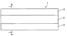
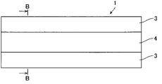
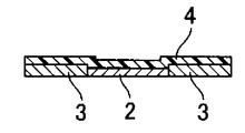
도 2a는, 도 1a의 다음의 제조 공정을 나타내는 평면도이며, 도 2b는, 도 2a를 B-B 선에 따라 절단하고 화살표 방향에서 본 단면도이며, 도 2c는, 도 2b와는 다른 구조의 단면도이다.
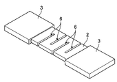
도 3a는, 도 2a 및 도 2b의 다음의 제조 공정을 나타내는 평면도이며, 도 3b는, 도 3a의 공정에서 잘라낸 저항기 중간체의 사시도이다.
도 4는, 도 3b의 다음의 제조 공정을 나타내는 사시도이다.
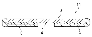
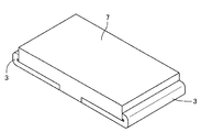
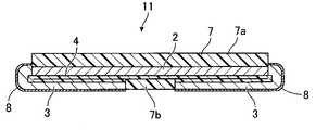
도 5a는, 도 4의 다음의 제조 공정을 나타내는 사시도이며, 도 5b는, 도 5a를 C-C 선에 따라 두께 방향으로 절단하고 화살표 방향에서 본 단면도이며, 도 5c는, 도 2b에 도시하는 적층 구조의 저항기 중간체를 이용하여 형성된 단면도이다.
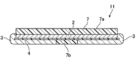
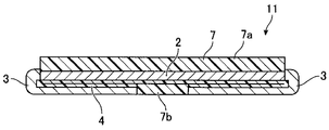
도 6a는, 도 5a의 다음의 제조 공정을 나타내는 사시도이며, 도 6b는, 도 5b의 다음의 제조 공정을 나타내는 단면도이며, 도 6c는, 도 5c의 다음의 제조 공정을 나타내는 단면도이다.
도 7a는, 도 6a의 다음의 제조 공정을 나타내는 사시도이며, 도 7b는, 도 6b의 다음의 제조 공정을 나타내는 단면도이며, 도 7c는, 도 6c의 다음의 제조 공정을 나타내는 단면도이다.
도 8은 폴리이미드·에폭시 수지의 DSC 곡선 및 DDSC 곡선을 나타내는 그래프이다.
도 9는 온도를 170℃로 고정했을 때의, 폴리이미드·에폭시 수지의 DSC 곡선을 나타내는 그래프이다.
Claims (4)
- 저항체의 표면에, 미경화인 열전도층을 형성하는 공정;
상기 열전도층을 반경화시키는 공정;
상기 저항체의 양측에 배치된 전극판을 절곡시켜, 상기 열전도층을 더욱 경화시켜, 상기 저항체와 전극판과의 사이를, 상기 열전도층을 통해 접착하는 공정;을 갖는 것을 특징으로 하는 저항기의 제조 방법. - 제 1항에 있어서,
상기 열전도층에는, 미경화이고 고화된 상태인 것을 이용하는 것을 특징으로 하는 저항기의 제조 방법. - 제 2항에 있어서,
상기 열전도층은, 열전도성 수지 필름인 것을 특징으로 하는 저항기의 제조 방법. - 제 1항 내지 제 3항 중 어느 한 항에 있어서,
절곡시킨 상기 전극판에 압력을 가하면서 상기 열전도층을 경화시키는 것을 특징으로 하는 저항기의 제조 방법.
Applications Claiming Priority (3)
| Application Number | Priority Date | Filing Date | Title |
|---|---|---|---|
| JPJP-P-2017-237821 | 2017-12-12 | ||
| JP2017237821A JP6573957B2 (ja) | 2017-12-12 | 2017-12-12 | 抵抗器の製造方法 |
| PCT/JP2018/045457 WO2019117128A1 (ja) | 2017-12-12 | 2018-12-11 | 抵抗器の製造方法 |
Publications (2)
| Publication Number | Publication Date |
|---|---|
| KR20200090867A true KR20200090867A (ko) | 2020-07-29 |
| KR102296639B1 KR102296639B1 (ko) | 2021-09-02 |
Family
ID=66819626
Family Applications (1)
| Application Number | Title | Priority Date | Filing Date |
|---|---|---|---|
| KR1020207018162A Active KR102296639B1 (ko) | 2017-12-12 | 2018-12-11 | 저항기의 제조 방법 |
Country Status (6)
| Country | Link |
|---|---|
| US (1) | US10892074B2 (ko) |
| EP (1) | EP3726542B1 (ko) |
| JP (1) | JP6573957B2 (ko) |
| KR (1) | KR102296639B1 (ko) |
| CN (1) | CN111465999B (ko) |
| WO (1) | WO2019117128A1 (ko) |
Families Citing this family (2)
| Publication number | Priority date | Publication date | Assignee | Title |
|---|---|---|---|---|
| US11011290B2 (en) * | 2017-12-12 | 2021-05-18 | Koa Corporation | Method for manufacturing resistor, and resistor |
| DE102022113553A1 (de) * | 2022-05-30 | 2023-11-30 | Isabellenhütte Heusler Gmbh & Co. Kg | Herstellungsverfahren für einen elektrischen Widerstand |
Citations (4)
| Publication number | Priority date | Publication date | Assignee | Title |
|---|---|---|---|---|
| US4806421A (en) | 1986-06-09 | 1989-02-21 | Mitsubishi Paper Mills, Ltd. | Thermal transfer recording sheet |
| JPH09181448A (ja) * | 1995-12-25 | 1997-07-11 | Matsushita Electric Works Ltd | 多層配線板の製造方法 |
| JP2008532280A (ja) * | 2005-02-25 | 2008-08-14 | ヴィスハイ デール エレクトロニクス,インコーポレーテッド | 熱的に伝導性で、電気的に非伝導性の充填材を備えた表面実装電気抵抗器およびそれを製作する方法 |
| JP2015008316A (ja) * | 2005-11-07 | 2015-01-15 | タイコエレクトロニクスジャパン合同会社 | Ptcデバイス |
Family Cites Families (26)
| Publication number | Priority date | Publication date | Assignee | Title |
|---|---|---|---|---|
| US2745931A (en) * | 1953-03-25 | 1956-05-15 | Erie Resistor Corp | Resistors and method of making the same |
| JPS6015319Y2 (ja) * | 1976-07-19 | 1985-05-14 | 北陸電気工業株式会社 | リ−ドフレ−ム |
| DE3027122A1 (de) * | 1980-07-17 | 1982-02-11 | Siemens AG, 1000 Berlin und 8000 München | Chip-widerstand |
| JPS59177929U (ja) * | 1983-05-13 | 1984-11-28 | 日本電気株式会社 | 樹脂外装形電子部品 |
| DE4143217A1 (de) * | 1991-01-18 | 1992-07-23 | Tech Wissenschaftliche Ges Thi | Chipwiderstand und chip-leiterbahnbruecke in duennschichttechnik und verfahren zu deren herstellung |
| US5179366A (en) * | 1991-06-24 | 1993-01-12 | Motorola, Inc. | End terminated high power chip resistor assembly |
| DE4202824C2 (de) * | 1992-01-31 | 1995-01-05 | Fraunhofer Ges Forschung | Chip-Bauelement und Verfahren zu dessen Herstellung |
| DE4339551C1 (de) * | 1993-11-19 | 1994-10-13 | Heusler Isabellenhuette | Widerstand in SMD-Bauweise und Verfahren zu seiner Herstellung sowie Leiterplatte mit solchem Widerstand |
| US5739743A (en) * | 1996-02-05 | 1998-04-14 | Emc Technology, Inc. | Asymmetric resistor terminal |
| JP3846986B2 (ja) * | 1997-11-21 | 2006-11-15 | 北陸電気工業株式会社 | チップ抵抗器の製造方法 |
| TW404969B (en) | 1998-02-23 | 2000-09-11 | Asahi Chemical Ind | Curable polyphenylene ether resin composition and the uses thereof |
| JP2003272453A (ja) * | 2002-03-13 | 2003-09-26 | Kanegafuchi Chem Ind Co Ltd | 半導電性無機フィラー及びその製造方法ならびに半導電性樹脂組成物 |
| JP4012029B2 (ja) * | 2002-09-30 | 2007-11-21 | コーア株式会社 | 金属板抵抗器およびその製造方法 |
| US20040156177A1 (en) | 2003-02-12 | 2004-08-12 | Matsushita Electric Industrial Co., Ltd. | Package of electronic components and method for producing the same |
| JP4128106B2 (ja) * | 2003-05-21 | 2008-07-30 | 北陸電気工業株式会社 | シャント抵抗器及びその製造方法 |
| WO2007043360A1 (ja) * | 2005-10-11 | 2007-04-19 | Murata Manufacturing Co., Ltd. | 正特性サーミスタ装置 |
| WO2009041974A1 (en) * | 2007-09-27 | 2009-04-02 | Vishay Dale Electronics, Inc. | Power resistor |
| US8325007B2 (en) * | 2009-12-28 | 2012-12-04 | Vishay Dale Electronics, Inc. | Surface mount resistor with terminals for high-power dissipation and method for making same |
| US8872358B2 (en) * | 2012-02-07 | 2014-10-28 | Shin-Etsu Chemical Co., Ltd. | Sealant laminated composite, sealed semiconductor devices mounting substrate, sealed semiconductor devices forming wafer, semiconductor apparatus, and method for manufacturing semiconductor apparatus |
| US8823483B2 (en) * | 2012-12-21 | 2014-09-02 | Vishay Dale Electronics, Inc. | Power resistor with integrated heat spreader |
| JP6519085B2 (ja) * | 2013-09-25 | 2019-05-29 | リンテック株式会社 | 熱伝導性接着シート、その製造方法及びそれを用いた電子デバイス |
| US20150194553A1 (en) * | 2014-01-08 | 2015-07-09 | Taiflex Scientific Co., Ltd. | Thermally conductive encapsulate and solar cell module comprising the same |
| US11438973B2 (en) * | 2014-04-10 | 2022-09-06 | Metis Design Corporation | Multifunctional assemblies |
| TWI600354B (zh) * | 2014-09-03 | 2017-09-21 | 光頡科技股份有限公司 | 具高彎折力之微電阻結構及其製造方法 |
| KR101853170B1 (ko) * | 2015-12-22 | 2018-04-27 | 삼성전기주식회사 | 칩 저항기 및 그 제조 방법 |
| US10438729B2 (en) * | 2017-11-10 | 2019-10-08 | Vishay Dale Electronics, Llc | Resistor with upper surface heat dissipation |
-
2017
- 2017-12-12 JP JP2017237821A patent/JP6573957B2/ja active Active
-
2018
- 2018-12-11 CN CN201880079884.0A patent/CN111465999B/zh active Active
- 2018-12-11 EP EP18888116.3A patent/EP3726542B1/en active Active
- 2018-12-11 KR KR1020207018162A patent/KR102296639B1/ko active Active
- 2018-12-11 WO PCT/JP2018/045457 patent/WO2019117128A1/ja not_active Ceased
- 2018-12-11 US US16/771,334 patent/US10892074B2/en active Active
Patent Citations (4)
| Publication number | Priority date | Publication date | Assignee | Title |
|---|---|---|---|---|
| US4806421A (en) | 1986-06-09 | 1989-02-21 | Mitsubishi Paper Mills, Ltd. | Thermal transfer recording sheet |
| JPH09181448A (ja) * | 1995-12-25 | 1997-07-11 | Matsushita Electric Works Ltd | 多層配線板の製造方法 |
| JP2008532280A (ja) * | 2005-02-25 | 2008-08-14 | ヴィスハイ デール エレクトロニクス,インコーポレーテッド | 熱的に伝導性で、電気的に非伝導性の充填材を備えた表面実装電気抵抗器およびそれを製作する方法 |
| JP2015008316A (ja) * | 2005-11-07 | 2015-01-15 | タイコエレクトロニクスジャパン合同会社 | Ptcデバイス |
Also Published As
| Publication number | Publication date |
|---|---|
| KR102296639B1 (ko) | 2021-09-02 |
| CN111465999B (zh) | 2022-04-15 |
| WO2019117128A1 (ja) | 2019-06-20 |
| JP6573957B2 (ja) | 2019-09-11 |
| EP3726542A1 (en) | 2020-10-21 |
| EP3726542B1 (en) | 2025-06-18 |
| EP3726542A4 (en) | 2021-09-01 |
| US20200343028A1 (en) | 2020-10-29 |
| CN111465999A (zh) | 2020-07-28 |
| JP2019106449A (ja) | 2019-06-27 |
| US10892074B2 (en) | 2021-01-12 |
Similar Documents
| Publication | Publication Date | Title |
|---|---|---|
| US9852836B2 (en) | Inductor and method for manufacturing the same | |
| US10181445B2 (en) | Power module | |
| JP6726821B2 (ja) | 半導体装置の製造方法 | |
| US20200411232A1 (en) | Inductor | |
| US20150061114A1 (en) | Semiconductor device and method of manufacturing the same | |
| US20210020557A1 (en) | Insulating circuit substrate and method for producing insulating circuit substrate | |
| KR102296639B1 (ko) | 저항기의 제조 방법 | |
| US11011290B2 (en) | Method for manufacturing resistor, and resistor | |
| KR102296732B1 (ko) | 저항기의 제조 방법 및 저항기 | |
| TWI552662B (zh) | A manufacturing method of a substrate in which an element is incorporated, and a substrate having a built-in element manufactured by the method | |
| JP2009117479A (ja) | コイル部品 | |
| US11291110B2 (en) | Resin substrate and electronic device | |
| JP3012875B2 (ja) | チップ抵抗器の製造方法 | |
| JP4566573B2 (ja) | 部品実装構造および部品実装方法 | |
| JP3749201B2 (ja) | プリント配線板の製造方法 | |
| JP3323156B2 (ja) | チップ抵抗器 | |
| WO2024095811A1 (ja) | 回路基板の製造方法 | |
| CN116487138A (zh) | 一种高精度的合金贴片电阻器的制作方法及其产品 | |
| JP2007201035A (ja) | 積層基板の製造方法 | |
| JP2020167234A (ja) | モジュールおよびその製造方法 | |
| WO2011093068A1 (ja) | 部品内蔵基板の製造方法および部品内蔵基板 |
Legal Events
| Date | Code | Title | Description |
|---|---|---|---|
| A201 | Request for examination | ||
| PA0105 | International application |
Patent event date: 20200623 Patent event code: PA01051R01D Comment text: International Patent Application |
|
| PA0201 | Request for examination | ||
| PG1501 | Laying open of application | ||
| E902 | Notification of reason for refusal | ||
| PE0902 | Notice of grounds for rejection |
Comment text: Notification of reason for refusal Patent event date: 20210602 Patent event code: PE09021S01D |
|
| E701 | Decision to grant or registration of patent right | ||
| PE0701 | Decision of registration |
Patent event code: PE07011S01D Comment text: Decision to Grant Registration Patent event date: 20210806 |
|
| GRNT | Written decision to grant | ||
| PR0701 | Registration of establishment |
Comment text: Registration of Establishment Patent event date: 20210826 Patent event code: PR07011E01D |
|
| PR1002 | Payment of registration fee |
Payment date: 20210827 End annual number: 3 Start annual number: 1 |
|
| PG1601 | Publication of registration | ||
| PR1001 | Payment of annual fee |
Payment date: 20240722 Start annual number: 4 End annual number: 4 |