KR20200092053A - 스위치 및 상기 스위치를 제어하기 위한 스위치 제어 프로세서를 포함하는 증폭기 - Google Patents
스위치 및 상기 스위치를 제어하기 위한 스위치 제어 프로세서를 포함하는 증폭기 Download PDFInfo
- Publication number
- KR20200092053A KR20200092053A KR1020190009121A KR20190009121A KR20200092053A KR 20200092053 A KR20200092053 A KR 20200092053A KR 1020190009121 A KR1020190009121 A KR 1020190009121A KR 20190009121 A KR20190009121 A KR 20190009121A KR 20200092053 A KR20200092053 A KR 20200092053A
- Authority
- KR
- South Korea
- Prior art keywords
- switch
- terminal
- electrically connected
- nmos
- pmos
- Prior art date
- Legal status (The legal status is an assumption and is not a legal conclusion. Google has not performed a legal analysis and makes no representation as to the accuracy of the status listed.)
- Granted
Links
Images


Classifications
-
- H—ELECTRICITY
- H03—ELECTRONIC CIRCUITRY
- H03G—CONTROL OF AMPLIFICATION
- H03G1/00—Details of arrangements for controlling amplification
- H03G1/0005—Circuits characterised by the type of controlling devices operated by a controlling current or voltage signal
- H03G1/0035—Circuits characterised by the type of controlling devices operated by a controlling current or voltage signal using continuously variable impedance elements
- H03G1/007—Circuits characterised by the type of controlling devices operated by a controlling current or voltage signal using continuously variable impedance elements using field-effect transistors [FET]
-
- H—ELECTRICITY
- H10—SEMICONDUCTOR DEVICES; ELECTRIC SOLID-STATE DEVICES NOT OTHERWISE PROVIDED FOR
- H10D—INORGANIC ELECTRIC SEMICONDUCTOR DEVICES
- H10D64/00—Electrodes of devices having potential barriers
- H10D64/60—Electrodes characterised by their materials
- H10D64/605—Source, drain, or gate electrodes for FETs comprising highly resistive materials
-
- H—ELECTRICITY
- H03—ELECTRONIC CIRCUITRY
- H03F—AMPLIFIERS
- H03F3/00—Amplifiers with only discharge tubes or only semiconductor devices as amplifying elements
- H03F3/189—High-frequency amplifiers, e.g. radio frequency amplifiers
- H03F3/19—High-frequency amplifiers, e.g. radio frequency amplifiers with semiconductor devices only
- H03F3/195—High-frequency amplifiers, e.g. radio frequency amplifiers with semiconductor devices only in integrated circuits
-
- H—ELECTRICITY
- H03—ELECTRONIC CIRCUITRY
- H03F—AMPLIFIERS
- H03F3/00—Amplifiers with only discharge tubes or only semiconductor devices as amplifying elements
- H03F3/45—Differential amplifiers
- H03F3/45071—Differential amplifiers with semiconductor devices only
- H03F3/45076—Differential amplifiers with semiconductor devices only characterised by the way of implementation of the active amplifying circuit in the differential amplifier
- H03F3/45475—Differential amplifiers with semiconductor devices only characterised by the way of implementation of the active amplifying circuit in the differential amplifier using IC blocks as the active amplifying circuit
-
- H—ELECTRICITY
- H03—ELECTRONIC CIRCUITRY
- H03G—CONTROL OF AMPLIFICATION
- H03G1/00—Details of arrangements for controlling amplification
- H03G1/0005—Circuits characterised by the type of controlling devices operated by a controlling current or voltage signal
- H03G1/0088—Circuits characterised by the type of controlling devices operated by a controlling current or voltage signal using discontinuously variable devices, e.g. switch-operated
-
- H—ELECTRICITY
- H03—ELECTRONIC CIRCUITRY
- H03G—CONTROL OF AMPLIFICATION
- H03G3/00—Gain control in amplifiers or frequency changers
- H03G3/20—Automatic control
- H03G3/30—Automatic control in amplifiers having semiconductor devices
- H03G3/3005—Automatic control in amplifiers having semiconductor devices in amplifiers suitable for low-frequencies, e.g. audio amplifiers
- H03G3/301—Automatic control in amplifiers having semiconductor devices in amplifiers suitable for low-frequencies, e.g. audio amplifiers the gain being continuously variable
- H03G3/3015—Automatic control in amplifiers having semiconductor devices in amplifiers suitable for low-frequencies, e.g. audio amplifiers the gain being continuously variable using diodes or transistors
-
- H—ELECTRICITY
- H03—ELECTRONIC CIRCUITRY
- H03K—PULSE TECHNIQUE
- H03K17/00—Electronic switching or gating, i.e. not by contact-making and –breaking
- H03K17/51—Electronic switching or gating, i.e. not by contact-making and –breaking characterised by the components used
- H03K17/56—Electronic switching or gating, i.e. not by contact-making and –breaking characterised by the components used by the use, as active elements, of semiconductor devices
- H03K17/687—Electronic switching or gating, i.e. not by contact-making and –breaking characterised by the components used by the use, as active elements, of semiconductor devices the devices being field-effect transistors
- H03K17/6871—Electronic switching or gating, i.e. not by contact-making and –breaking characterised by the components used by the use, as active elements, of semiconductor devices the devices being field-effect transistors the output circuit comprising more than one controlled field-effect transistor
- H03K17/6872—Electronic switching or gating, i.e. not by contact-making and –breaking characterised by the components used by the use, as active elements, of semiconductor devices the devices being field-effect transistors the output circuit comprising more than one controlled field-effect transistor using complementary field-effect transistors
-
- H—ELECTRICITY
- H03—ELECTRONIC CIRCUITRY
- H03K—PULSE TECHNIQUE
- H03K17/00—Electronic switching or gating, i.e. not by contact-making and –breaking
- H03K17/51—Electronic switching or gating, i.e. not by contact-making and –breaking characterised by the components used
- H03K17/56—Electronic switching or gating, i.e. not by contact-making and –breaking characterised by the components used by the use, as active elements, of semiconductor devices
- H03K17/687—Electronic switching or gating, i.e. not by contact-making and –breaking characterised by the components used by the use, as active elements, of semiconductor devices the devices being field-effect transistors
- H03K17/6877—Electronic switching or gating, i.e. not by contact-making and –breaking characterised by the components used by the use, as active elements, of semiconductor devices the devices being field-effect transistors the control circuit comprising active elements different from those used in the output circuit
-
- H—ELECTRICITY
- H03—ELECTRONIC CIRCUITRY
- H03K—PULSE TECHNIQUE
- H03K17/00—Electronic switching or gating, i.e. not by contact-making and –breaking
- H03K17/51—Electronic switching or gating, i.e. not by contact-making and –breaking characterised by the components used
- H03K17/56—Electronic switching or gating, i.e. not by contact-making and –breaking characterised by the components used by the use, as active elements, of semiconductor devices
- H03K17/687—Electronic switching or gating, i.e. not by contact-making and –breaking characterised by the components used by the use, as active elements, of semiconductor devices the devices being field-effect transistors
- H03K17/693—Switching arrangements with several input- or output-terminals, e.g. multiplexers, distributors
-
- H—ELECTRICITY
- H10—SEMICONDUCTOR DEVICES; ELECTRIC SOLID-STATE DEVICES NOT OTHERWISE PROVIDED FOR
- H10D—INORGANIC ELECTRIC SEMICONDUCTOR DEVICES
- H10D62/00—Semiconductor bodies, or regions thereof, of devices having potential barriers
- H10D62/10—Shapes, relative sizes or dispositions of the regions of the semiconductor bodies; Shapes of the semiconductor bodies
- H10D62/17—Semiconductor regions connected to electrodes not carrying current to be rectified, amplified or switched, e.g. channel regions
- H10D62/213—Channel regions of field-effect devices
- H10D62/221—Channel regions of field-effect devices of FETs
- H10D62/328—Channel regions of field-effect devices of FETs having PN junction gates
Landscapes
- Engineering & Computer Science (AREA)
- Power Engineering (AREA)
- Microelectronics & Electronic Packaging (AREA)
- Multimedia (AREA)
- Electronic Switches (AREA)
Abstract
본 발명은 입력단에 전기적으로 연결된 제1 저항, 출력단에 전기적으로 연결된 제2 저항 모스펫(MOSFET)으로 구성되고 상기 제2 저항의 일단과 전기적으로 연결되는 스위치 및 상기 스위치를 구성하는 모스펫의 게이트단과 상기 스위치를 구성하는 모스펫의 벌크(bulk)단이 기설정된 제1 문턱값보다 높은 임피던스값을 가지는 임피던스와 전기적으로 연결되도록 형성된 스위치 제어 프로세서를 포함하는 증폭기를 제공한다.
Description
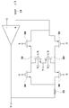
도 1b는 종래 기술에 따른 증폭기의 스위치를 제어하기 위한 스위치 제어 프로세서를 나타낸 도면이다.
도 2a는 본 개시에서 개시하고 있는 일 실시예에 따른 스위치 제어 프로세서를 나타낸 도면이다.
도 2b는 본 개시에서 개시하고 있는 일 실시예에 따른 증폭기를 나타낸 도면이다.
도 3a는 본 개시에서 개시하고 있는 일 실시예에 따라 2단 스위치 및 단락 스위치를 포함하는 증폭기를 나타낸 도면이다.
도 3b는 본 개시에서 개시하고 있는 일 실시예에 따른 2단 스위치 및 단락 스위치를 제어하기 위한 스위치 제어 프로세서를 나타낸 도면이다.
도 4는 본 개시에서 개시하고 있는 일 실시예에 따라 단락 스위치를 PMOS와 NMOS로 구성한 경우를 나타낸 도면이다.
도 5는 본 개시에서 개시하고 있는 일 실시예에 따른 가변 이득 증폭기를 나타낸 도면이다.
Claims (20)
- 입력신호를 증폭하는 증폭기에 있어서,
입력단에 전기적으로 연결된 제1 저항;
출력단에 전기적으로 연결된 제2 저항;
모스펫(MOSFET)으로 구성되고 상기 제2 저항의 일단과 전기적으로 연결되는 스위치; 및
상기 스위치를 구성하는 모스펫의 게이트단과 상기 스위치를 구성하는 모스펫의 벌크(bulk)단이 기설정된 제1 문턱값보다 높은 임피던스값을 가지는 임피던스와 전기적으로 연결되도록 형성된 스위치 제어 프로세서를 포함하는,
증폭기. - 제1항에 있어서,
상기 스위치는 CMOS(complementary metal-oxide semiconductor)를 포함하고,
상기 스위치 제어 프로세서는,
상기 CMOS를 구성하는 PMOS의 게이트단과 상기 PMOS의 벌크단이 상기 제1 문턱값보다 높은 임피던스값을 가지는 제1 임피던스; 및
상기 CMOS를 구성하는 NMOS의 게이트단과 상기 NMOS의 벌크단이 상기 제1 문턱값보다 높은 임피던스값을 가지는 제2 임피던스를 포함하는 것을 특징으로 하는,
증폭기. - 제2항에 있어서,
상기 스위치 제어 프로세서는,
제어 신호를 수신하는 제1 인버터;
제1 PMOS의 게이트단과 제1 NMOS의 게이트단이 상기 제1 인버터의 출력단과 전기적으로 연결되는 제1 CMOS;
상기 제1 인버터의 출력단과 전기적으로 연결되는 제2 인버터;
제2 PMOS의 게이트단과 제2 NMOS의 게이트단이 상기 제2 인버터의 출력단과 전기적으로 연결되는 제2 CMOS;
상기 제1 PMOS의 소스단 및 상기 제2 PMOS의 소스단과 전기적으로 연결되고 상기 제1 문턱값보다 높은 임피던스값을 가지는 제1 임피던스; 및
상기 제1 NMOS의 소스단 및 상기 제2 NMOS의 소스단과 전기적으로 연결되고 상기 제1 문턱값보다 높은 임피던스값을 가지는 제2 임피던스를 포함하는 것을 특징으로 하는,
증폭기. - 제3항에 있어서,
상기 스위치를 구성하는 PMOS의 벌크단은 상기 제1 PMOS의 소스단 또는 상기 제2 PMOS의 소스단과 전기적으로 연결되고, 상기 스위치를 구성하는 NMOS의 벌크단은 상기 제1 NMOS의 소스단 또는 상기 제2 NMOS의 소스단과 전기적으로 연결되는 것을 특징으로 하는,
증폭기. - 제3항에 있어서,
상기 스위치를 구성하는 PMOS의 게이트단은 상기 제1 CMOS의 출력단과 전기적으로 연결되고, 상기 스위치를 구성하는 NMOS의 게이트단은 상기 제2 CMOS의 출력단과 전기적으로 연결되는 것을 특징으로 하는,
증폭기. - 제1항에 있어서,
상기 스위치는,
CMOS로 구성되며 상기 제2 저항의 일단과 전기적으로 연결되는 제1 스위치; 및
CMOS로 구성되며 상기 제1 스위치의 일단과 전기적으로 연결되는 제2 스위치를 포함하는 것을 특징으로 하는,
증폭기. - 제6항에 있어서,
상기 스위치 제어 프로세서는,
제어 신호를 수신하는 제1 인버터;
제1 PMOS의 게이트단과 제1 NMOS의 게이트단이 상기 제1 인버터의 출력단과 전기적으로 연결되는 제1 CMOS;
상기 제1 인버터의 출력단과 전기적으로 연결되는 제2 인버터;
제2 PMOS의 게이트단과 제2 NMOS의 게이트단이 상기 제2 인버터의 출력단과 전기적으로 연결되는 제2 CMOS;
상기 제1 PMOS의 소스단 및 상기 제2 PMOS의 소스단과 전기적으로 연결되고 상기 제1 문턱값보다 높은 임피던스값을 가지는 제1 임피던스;
상기 제1 NMOS의 소스단 및 상기 제2 NMOS의 소스단과 전기적으로 연결되고 상기 제1 문턱값보다 높은 임피던스값을 가지는 제2 임피던스;
제3 PMOS의 게이트단과 제3 NMOS의 게이트단이 상기 제1 인버터의 출력단과 전기적으로 연결되는 제3 CMOS;
제4 PMOS의 게이트단과 제4 NMOS의 게이트단이 상기 제2 인버터의 출력단과 전기적으로 연결되는 제4 CMOS;
상기 제3 PMOS의 소스단 및 상기 제4 PMOS의 소스단과 전기적으로 연결되고 상기 제1 문턱값보다 높은 임피던스값을 가지는 제3 임피던스; 및
상기 제3 NMOS의 소스단 및 상기 제4 NMOS의 소스단과 전기적으로 연결되고 상기 제1 문턱값보다 높은 임피던스값을 가지는 제4 임피던스를 포함하는,
증폭기. - 제7항에 있어서,
상기 제1 스위치를 구성하는 PMOS의 벌크단은 상기 제1 PMOS의 소스단 또는 상기 제2 PMOS의 소스단과 전기적으로 연결되고, 상기 제1 스위치를 구성하는 NMOS의 벌크단은 상기 제1 NMOS의 소스단 또는 상기 제2 NMOS의 소스단과 전기적으로 연결되며, 상기 제2 스위치를 구성하는 PMOS의 벌크단은 상기 제3 PMOS의 소스단 또는 상기 제4 PMOS의 소스단과 전기적으로 연결되고, 상기 제2 스위치를 구성하는 NMOS의 벌크단은 상기 제3 NMOS의 소스단 또는 상기 제4 NMOS의 소스단과 전기적으로 연결되는 것을 특징으로 하는,
증폭기. - 제6항에 있어서,
상기 제1 스위치와 상기 제2 스위치 사이에 기설정된 제2 문턱값보다 낮은 임피던스값을 가지는 제3 스위치를 더 포함하는,
증폭기. - 제9항에 있어서,
상기 제3 스위치는,
상기 제2 문턱값보다 낮은 임피던스값을 가지며, 상기 제1 스위치를 구성하는 PMOS와 상기 제2 스위치를 구성하는 PMOS 사이에 드레인단이 전기적으로 연결되는 제5 PMOS; 및
상기 제2 문턱값보다 낮은 임피던스값을 가지며, 상기 제1 스위치를 구성하는 NMOS와 상기 제2 스위치를 구성하는 NMOS 사이에 드레인단이 전기적으로 연결되는 제5 NMOS를 포함하는 것을 특징으로 하는,
증폭기. - 증폭기를 포함하는 전자 장치에 있어서,
상기 증폭기는,
입력단에 전기적으로 연결된 제1 저항;
출력단에 전기적으로 연결된 제2 저항;
모스펫(MOSFET)으로 구성되고 상기 제2 저항의 일단과 전기적으로 연결되는 스위치; 및
상기 스위치를 구성하는 모스펫의 게이트단과 상기 스위치를 구성하는 모스펫의 벌크(bulk)단이 기설정된 제1 문턱값보다 높은 임피던스값을 가지는 임피던스와 전기적으로 연결되도록 형성된 스위치 제어 프로세서를 포함하는 것을 특징으로 하는,
전자 장치. - 제11항에 있어서,
상기 스위치는 CMOS(complementary metal-oxide semiconductor)를 포함하고,
상기 스위치 제어 프로세서는,
상기 CMOS를 구성하는 PMOS의 게이트단과 상기 PMOS의 벌크단이 상기 제1 문턱값보다 높은 임피던스값을 가지는 제1 임피던스; 및
상기 CMOS를 구성하는 NMOS의 게이트단과 상기 NMOS의 벌크단이 상기 제1 문턱값보다 높은 임피던스값을 가지는 제2 임피던스를 포함하는 것을 특징으로 하는,
전자 장치. - 제12항에 있어서,
상기 스위치 제어 프로세서는,
제어 신호를 수신하는 제1 인버터;
제1 PMOS의 게이트단과 제1 NMOS의 게이트단이 상기 제1 인버터의 출력단과 전기적으로 연결되는 제1 CMOS;
상기 제1 인버터의 출력단과 전기적으로 연결되는 제2 인버터;
제2 PMOS의 게이트단과 제2 NMOS의 게이트단이 상기 제2 인버터의 출력단과 전기적으로 연결되는 제2 CMOS;
상기 제1 PMOS의 소스단 및 상기 제2 PMOS의 소스단과 전기적으로 연결되고 상기 제1 문턱값보다 높은 임피던스값을 가지는 제1 임피던스; 및
상기 제1 NMOS의 소스단 및 상기 제2 NMOS의 소스단과 전기적으로 연결되고 상기 제1 문턱값보다 높은 임피던스값을 가지는 제2 임피던스를 포함하는 것을 특징으로 하는,
전자 장치. - 제13항에 있어서,
상기 스위치를 구성하는 PMOS의 벌크단은 상기 제1 PMOS의 소스단 또는 상기 제2 PMOS의 소스단과 전기적으로 연결되고, 상기 스위치를 구성하는 NMOS의 벌크단은 상기 제1 NMOS의 소스단 또는 상기 제2 NMOS의 소스단과 전기적으로 연결되는 것을 특징으로 하는,
전자 장치. - 제13항에 있어서,
상기 스위치를 구성하는 PMOS의 게이트단은 상기 제1 CMOS의 출력단과 전기적으로 연결되고, 상기 스위치를 구성하는 NMOS의 게이트단은 상기 제2 CMOS의 출력단과 전기적으로 연결되는 것을 특징으로 하는,
전자 장치. - 제11항에 있어서,
상기 스위치는,
CMOS로 구성되며 상기 제2 저항의 일단과 전기적으로 연결되는 제1 스위치; 및
CMOS로 구성되며 상기 제1 스위치의 일단과 전기적으로 연결되는 제2 스위치를 포함하는 것을 특징으로 하는,
전자 장치. - 제16항에 있어서,
상기 스위치 제어 프로세서는,
제어 신호를 수신하는 제1 인버터;
제1 PMOS의 게이트단과 제1 NMOS의 게이트단이 상기 제1 인버터의 출력단과 전기적으로 연결되는 제1 CMOS;
상기 제1 인버터의 출력단과 전기적으로 연결되는 제2 인버터;
제2 PMOS의 게이트단과 제2 NMOS의 게이트단이 상기 제2 인버터의 출력단과 전기적으로 연결되는 제2 CMOS;
상기 제1 PMOS의 소스단 및 상기 제2 PMOS의 소스단과 전기적으로 연결되고 상기 제1 문턱값보다 높은 임피던스값을 가지는 제1 임피던스;
상기 제1 NMOS의 소스단 및 상기 제2 NMOS의 소스단과 전기적으로 연결되고 상기 제1 문턱값보다 높은 임피던스값을 가지는 제2 임피던스;
제3 PMOS의 게이트단과 제3 NMOS의 게이트단이 상기 제1 인버터의 출력단과 전기적으로 연결되는 제3 CMOS;
제4 PMOS의 게이트단과 제4 NMOS의 게이트단이 상기 제2 인버터의 출력단과 전기적으로 연결되는 제4 CMOS;
상기 제3 PMOS의 소스단 및 상기 제4 PMOS의 소스단과 전기적으로 연결되고 상기 제1 문턱값보다 높은 임피던스값을 가지는 제3 임피던스; 및
상기 제3 NMOS의 소스단 및 상기 제4 NMOS의 소스단과 전기적으로 연결되고 상기 제1 문턱값보다 높은 임피던스값을 가지는 제4 임피던스를 포함하는,
전자 장치. - 제17항에 있어서,
상기 제1 스위치를 구성하는 PMOS의 벌크단은 상기 제1 PMOS의 소스단 또는 상기 제2 PMOS의 소스단과 전기적으로 연결되고, 상기 제1 스위치를 구성하는 NMOS의 벌크단은 상기 제1 NMOS의 소스단 또는 상기 제2 NMOS의 소스단과 전기적으로 연결되며, 상기 제2 스위치를 구성하는 PMOS의 벌크단은 상기 제3 PMOS의 소스단 또는 상기 제4 PMOS의 소스단과 전기적으로 연결되고, 상기 제2 스위치를 구성하는 NMOS의 벌크단은 상기 제3 NMOS의 소스단 또는 상기 제4 NMOS의 소스단과 전기적으로 연결되는 것을 특징으로 하는,
전자 장치. - 제16항에 있어서,
상기 제1 스위치와 상기 제2 스위치 사이에 기설정된 제2 문턱값보다 낮은 임피던스값을 가지는 제3 스위치를 더 포함하는,
전자 장치. - 제19항에 있어서,
상기 제3 스위치는,
상기 제2 문턱값보다 낮은 임피던스값을 가지며, 상기 제1 스위치를 구성하는 PMOS와 상기 제2 스위치를 구성하는 PMOS 사이에 드레인단이 전기적으로 연결되는 제5 PMOS; 및
상기 제2 문턱값보다 낮은 임피던스값을 가지며, 상기 제1 스위치를 구성하는 NMOS와 상기 제2 스위치를 구성하는 NMOS 사이에 드레인단이 전기적으로 연결되는 제5 NMOS를 포함하는 것을 특징으로 하는,
전자 장치.
Priority Applications (4)
| Application Number | Priority Date | Filing Date | Title |
|---|---|---|---|
| KR1020190009121A KR102670924B1 (ko) | 2019-01-24 | 2019-01-24 | 스위치 및 상기 스위치를 제어하기 위한 스위치 제어 프로세서를 포함하는 증폭기 |
| PCT/KR2020/001149 WO2020153777A1 (en) | 2019-01-24 | 2020-01-23 | Amplifier having switch and switch control processor controlling switch |
| US16/750,826 US11227930B2 (en) | 2019-01-24 | 2020-01-23 | Amplifier having switch and switch control processor controlling switch |
| EP20744452.2A EP3861634B1 (en) | 2019-01-24 | 2020-01-23 | Amplifier having switch and switch control processor controlling switch |
Applications Claiming Priority (1)
| Application Number | Priority Date | Filing Date | Title |
|---|---|---|---|
| KR1020190009121A KR102670924B1 (ko) | 2019-01-24 | 2019-01-24 | 스위치 및 상기 스위치를 제어하기 위한 스위치 제어 프로세서를 포함하는 증폭기 |
Publications (2)
| Publication Number | Publication Date |
|---|---|
| KR20200092053A true KR20200092053A (ko) | 2020-08-03 |
| KR102670924B1 KR102670924B1 (ko) | 2024-05-31 |
Family
ID=71731966
Family Applications (1)
| Application Number | Title | Priority Date | Filing Date |
|---|---|---|---|
| KR1020190009121A Active KR102670924B1 (ko) | 2019-01-24 | 2019-01-24 | 스위치 및 상기 스위치를 제어하기 위한 스위치 제어 프로세서를 포함하는 증폭기 |
Country Status (4)
| Country | Link |
|---|---|
| US (1) | US11227930B2 (ko) |
| EP (1) | EP3861634B1 (ko) |
| KR (1) | KR102670924B1 (ko) |
| WO (1) | WO2020153777A1 (ko) |
Citations (2)
| Publication number | Priority date | Publication date | Assignee | Title |
|---|---|---|---|---|
| KR20080005139A (ko) * | 2006-07-07 | 2008-01-10 | 엔이씨 일렉트로닉스 가부시키가이샤 | 아날로그 및 디지털 신호 모두에 적합한 입력 인터페이스회로 |
| US20090179695A1 (en) * | 2008-01-11 | 2009-07-16 | Infineon Technologies Ag | Apparatus and method having reduced flicker noise |
Family Cites Families (14)
| Publication number | Priority date | Publication date | Assignee | Title |
|---|---|---|---|---|
| US5369711A (en) * | 1990-08-31 | 1994-11-29 | Bellsouth Corporation | Automatic gain control for a headset |
| JPH0661766A (ja) * | 1992-08-04 | 1994-03-04 | Nec Corp | 出力バッファアンプ回路 |
| JP3573849B2 (ja) | 1995-11-10 | 2004-10-06 | 富士通株式会社 | 増幅回路 |
| TWI268657B (en) | 2003-03-27 | 2006-12-11 | Realtek Semiconductor Corp | Variable gain amplifier |
| JP4460862B2 (ja) * | 2003-09-05 | 2010-05-12 | ヴェリジー(シンガポール) プライベート リミテッド | 半導体スイッチを用いた増幅装置 |
| JP2008187329A (ja) | 2007-01-29 | 2008-08-14 | Sony Corp | 可変利得増幅回路および可変利得アンプの入力インピーダンスマッチング方法 |
| EP2110947B1 (en) | 2008-04-18 | 2012-07-04 | St Microelectronics S.A. | Variable gain RF amplifier |
| JP2011124647A (ja) | 2009-12-08 | 2011-06-23 | Panasonic Corp | 可変利得増幅器 |
| US20130154740A1 (en) | 2011-12-16 | 2013-06-20 | Qualcomm Incorporated | Techniques for pga linearity |
| TWI624110B (zh) | 2012-07-07 | 2018-05-11 | Skyworks Solutions, Inc. | 與基於射頻開關之絕緣體上矽相關之電路、裝置、方法及其組合 |
| JP6466678B2 (ja) | 2014-10-01 | 2019-02-06 | ルネサスエレクトロニクス株式会社 | 半導体集積回路、可変利得増幅器、及び、センサシステム |
| US10560061B2 (en) * | 2016-09-01 | 2020-02-11 | Analog Devices, Inc. | Low capacitance switch for programmable gain amplifier or programable gain instrumentation amplifier |
| WO2018045298A1 (en) * | 2016-09-01 | 2018-03-08 | Analog Devices, Inc. | Low capacitance switch for pga or pgia |
| JP2018050238A (ja) | 2016-09-23 | 2018-03-29 | ルネサスエレクトロニクス株式会社 | 可変利得増幅器、方法、および受信装置 |
-
2019
- 2019-01-24 KR KR1020190009121A patent/KR102670924B1/ko active Active
-
2020
- 2020-01-23 US US16/750,826 patent/US11227930B2/en active Active
- 2020-01-23 EP EP20744452.2A patent/EP3861634B1/en active Active
- 2020-01-23 WO PCT/KR2020/001149 patent/WO2020153777A1/en not_active Ceased
Patent Citations (2)
| Publication number | Priority date | Publication date | Assignee | Title |
|---|---|---|---|---|
| KR20080005139A (ko) * | 2006-07-07 | 2008-01-10 | 엔이씨 일렉트로닉스 가부시키가이샤 | 아날로그 및 디지털 신호 모두에 적합한 입력 인터페이스회로 |
| US20090179695A1 (en) * | 2008-01-11 | 2009-07-16 | Infineon Technologies Ag | Apparatus and method having reduced flicker noise |
Also Published As
| Publication number | Publication date |
|---|---|
| US20200243661A1 (en) | 2020-07-30 |
| EP3861634B1 (en) | 2025-03-05 |
| KR102670924B1 (ko) | 2024-05-31 |
| EP3861634A1 (en) | 2021-08-11 |
| US11227930B2 (en) | 2022-01-18 |
| WO2020153777A1 (en) | 2020-07-30 |
| EP3861634A4 (en) | 2022-01-12 |
Similar Documents
| Publication | Publication Date | Title |
|---|---|---|
| KR102667414B1 (ko) | 무선 통신 시스템에서 네트워크 슬라이스의 상호 배타적 접속 방법 | |
| Pang et al. | A new 5G radio evolution towards 5G-Advanced | |
| KR102458844B1 (ko) | 전압 보상형 스위치 스택 | |
| CN111727645B (zh) | 基站、终端、基站的方法和终端的方法 | |
| Nawaz et al. | Next-generation consumer electronics for 6G wireless era | |
| KR102096331B1 (ko) | 오프-상태 커패시턴스 감소를 지닌 멀티-스루 안테나 스위치 | |
| KR20170054046A (ko) | 무선 통신 시스템에서 복호화 방법 및 장치 | |
| US9024796B2 (en) | Radio frequency digital to analog converter | |
| KR20190123801A (ko) | 폴라 코드의 부호율 조정 방법 및 장치 | |
| US12009566B2 (en) | Four-way power divider and combiner for phased array system | |
| CN113169712B (zh) | 用于切断漏电流的放大器和包括放大器的电子装置 | |
| US10826198B2 (en) | Circuit and method for adjusting frequency band of antenna, and electronic device | |
| KR20180070380A (ko) | 다층 인쇄 회로 기판 및 이를 포함하는 전자 장치 | |
| CN111247776A (zh) | 通信装置 | |
| KR20200092053A (ko) | 스위치 및 상기 스위치를 제어하기 위한 스위치 제어 프로세서를 포함하는 증폭기 | |
| TW202046648A (zh) | 鄰頻信號干擾消除方法、裝置及小型基站 | |
| US10763789B2 (en) | Mixer for reducing local frequency signal generated at output of the mixer | |
| US11477786B2 (en) | Method and an apparatus for determining a local frequency in wireless communication system | |
| US20200204202A1 (en) | Electronic device including plurality of antenna arrays | |
| KR20200085614A (ko) | 후왜곡을 이용한 선형화 증폭기 | |
| US20210194603A1 (en) | Base station and control method therefor in wireless communication system | |
| CN112262499B (zh) | 利用传输线长度的天线模块及包括该天线模块的电子设备 | |
| KR102477829B1 (ko) | 인쇄 회로 기판을 포함하는 컨버터 및 상기 컨버터를 포함하는 전력 변환 모듈 | |
| CN119012364B (zh) | 终端能力上报方法、用户终端、通信系统和存储介质 | |
| KR20230075466A (ko) | 무선 통신 시스템에서 단말 및 기지국의 채널 코딩 수행 방법 및 장치 |
Legal Events
| Date | Code | Title | Description |
|---|---|---|---|
| PA0109 | Patent application |
Patent event code: PA01091R01D Comment text: Patent Application Patent event date: 20190124 |
|
| PG1501 | Laying open of application | ||
| A201 | Request for examination | ||
| PA0201 | Request for examination |
Patent event code: PA02012R01D Patent event date: 20220103 Comment text: Request for Examination of Application Patent event code: PA02011R01I Patent event date: 20190124 Comment text: Patent Application |
|
| E902 | Notification of reason for refusal | ||
| PE0902 | Notice of grounds for rejection |
Comment text: Notification of reason for refusal Patent event date: 20231221 Patent event code: PE09021S01D |
|
| E701 | Decision to grant or registration of patent right | ||
| PE0701 | Decision of registration |
Patent event code: PE07011S01D Comment text: Decision to Grant Registration Patent event date: 20240226 |
|
| GRNT | Written decision to grant | ||
| PR0701 | Registration of establishment |
Comment text: Registration of Establishment Patent event date: 20240527 Patent event code: PR07011E01D |
|
| PR1002 | Payment of registration fee |
Payment date: 20240528 End annual number: 3 Start annual number: 1 |
|
| PG1601 | Publication of registration |