KR20200092402A - Overlay measurement of overlapping target structures based on the symmetry of the scanning electron beam signal - Google Patents
Overlay measurement of overlapping target structures based on the symmetry of the scanning electron beam signal Download PDFInfo
- Publication number
- KR20200092402A KR20200092402A KR1020207019931A KR20207019931A KR20200092402A KR 20200092402 A KR20200092402 A KR 20200092402A KR 1020207019931 A KR1020207019931 A KR 1020207019931A KR 20207019931 A KR20207019931 A KR 20207019931A KR 20200092402 A KR20200092402 A KR 20200092402A
- Authority
- KR
- South Korea
- Prior art keywords
- layer
- overlay
- symmetric
- scan signal
- measurements
- Prior art date
- Legal status (The legal status is an assumption and is not a legal conclusion. Google has not performed a legal analysis and makes no representation as to the accuracy of the status listed.)
- Granted
Links
Images


Classifications
-
- G—PHYSICS
- G03—PHOTOGRAPHY; CINEMATOGRAPHY; ANALOGOUS TECHNIQUES USING WAVES OTHER THAN OPTICAL WAVES; ELECTROGRAPHY; HOLOGRAPHY
- G03F—PHOTOMECHANICAL PRODUCTION OF TEXTURED OR PATTERNED SURFACES, e.g. FOR PRINTING, FOR PROCESSING OF SEMICONDUCTOR DEVICES; MATERIALS THEREFOR; ORIGINALS THEREFOR; APPARATUS SPECIALLY ADAPTED THEREFOR
- G03F7/00—Photomechanical, e.g. photolithographic, production of textured or patterned surfaces, e.g. printing surfaces; Materials therefor, e.g. comprising photoresists; Apparatus specially adapted therefor
- G03F7/70—Microphotolithographic exposure; Apparatus therefor
- G03F7/70483—Information management; Active and passive control; Testing; Wafer monitoring, e.g. pattern monitoring
- G03F7/70605—Workpiece metrology
- G03F7/70616—Monitoring the printed patterns
- G03F7/70633—Overlay, i.e. relative alignment between patterns printed by separate exposures in different layers, or in the same layer in multiple exposures or stitching
-
- G—PHYSICS
- G01—MEASURING; TESTING
- G01B—MEASURING LENGTH, THICKNESS OR SIMILAR LINEAR DIMENSIONS; MEASURING ANGLES; MEASURING AREAS; MEASURING IRREGULARITIES OF SURFACES OR CONTOURS
- G01B15/00—Measuring arrangements characterised by the use of electromagnetic waves or particle radiation, e.g. by the use of microwaves, X-rays, gamma rays or electrons
-
- G—PHYSICS
- G01—MEASURING; TESTING
- G01N—INVESTIGATING OR ANALYSING MATERIALS BY DETERMINING THEIR CHEMICAL OR PHYSICAL PROPERTIES
- G01N21/00—Investigating or analysing materials by the use of optical means, i.e. using sub-millimetre waves, infrared, visible or ultraviolet light
- G01N21/84—Systems specially adapted for particular applications
- G01N21/8422—Investigating thin films, e.g. matrix isolation method
-
- G—PHYSICS
- G03—PHOTOGRAPHY; CINEMATOGRAPHY; ANALOGOUS TECHNIQUES USING WAVES OTHER THAN OPTICAL WAVES; ELECTROGRAPHY; HOLOGRAPHY
- G03F—PHOTOMECHANICAL PRODUCTION OF TEXTURED OR PATTERNED SURFACES, e.g. FOR PRINTING, FOR PROCESSING OF SEMICONDUCTOR DEVICES; MATERIALS THEREFOR; ORIGINALS THEREFOR; APPARATUS SPECIALLY ADAPTED THEREFOR
- G03F7/00—Photomechanical, e.g. photolithographic, production of textured or patterned surfaces, e.g. printing surfaces; Materials therefor, e.g. comprising photoresists; Apparatus specially adapted therefor
- G03F7/70—Microphotolithographic exposure; Apparatus therefor
- G03F7/70483—Information management; Active and passive control; Testing; Wafer monitoring, e.g. pattern monitoring
- G03F7/70605—Workpiece metrology
- G03F7/70616—Monitoring the printed patterns
- G03F7/70625—Dimensions, e.g. line width, critical dimension [CD], profile, sidewall angle or edge roughness
-
- G—PHYSICS
- G03—PHOTOGRAPHY; CINEMATOGRAPHY; ANALOGOUS TECHNIQUES USING WAVES OTHER THAN OPTICAL WAVES; ELECTROGRAPHY; HOLOGRAPHY
- G03F—PHOTOMECHANICAL PRODUCTION OF TEXTURED OR PATTERNED SURFACES, e.g. FOR PRINTING, FOR PROCESSING OF SEMICONDUCTOR DEVICES; MATERIALS THEREFOR; ORIGINALS THEREFOR; APPARATUS SPECIALLY ADAPTED THEREFOR
- G03F7/00—Photomechanical, e.g. photolithographic, production of textured or patterned surfaces, e.g. printing surfaces; Materials therefor, e.g. comprising photoresists; Apparatus specially adapted therefor
- G03F7/70—Microphotolithographic exposure; Apparatus therefor
- G03F7/70483—Information management; Active and passive control; Testing; Wafer monitoring, e.g. pattern monitoring
- G03F7/70605—Workpiece metrology
- G03F7/706843—Metrology apparatus
- G03F7/706847—Production of measurement radiation, e.g. synchrotron, free-electron laser, plasma source or higher harmonic generation [HHG]
-
- H—ELECTRICITY
- H01—ELECTRIC ELEMENTS
- H01J—ELECTRIC DISCHARGE TUBES OR DISCHARGE LAMPS
- H01J37/00—Discharge tubes with provision for introducing objects or material to be exposed to the discharge, e.g. for the purpose of examination or processing thereof
- H01J37/26—Electron or ion microscopes; Electron or ion diffraction tubes
-
- H—ELECTRICITY
- H01—ELECTRIC ELEMENTS
- H01J—ELECTRIC DISCHARGE TUBES OR DISCHARGE LAMPS
- H01J37/00—Discharge tubes with provision for introducing objects or material to be exposed to the discharge, e.g. for the purpose of examination or processing thereof
- H01J37/26—Electron or ion microscopes; Electron or ion diffraction tubes
- H01J37/28—Electron or ion microscopes; Electron or ion diffraction tubes with scanning beams
-
- H—ELECTRICITY
- H01—ELECTRIC ELEMENTS
- H01J—ELECTRIC DISCHARGE TUBES OR DISCHARGE LAMPS
- H01J37/00—Discharge tubes with provision for introducing objects or material to be exposed to the discharge, e.g. for the purpose of examination or processing thereof
- H01J37/30—Electron-beam or ion-beam tubes for localised treatment of objects
- H01J37/304—Controlling tubes by information coming from the objects or from the beam, e.g. correction signals
-
- H—ELECTRICITY
- H01—ELECTRIC ELEMENTS
- H01J—ELECTRIC DISCHARGE TUBES OR DISCHARGE LAMPS
- H01J37/00—Discharge tubes with provision for introducing objects or material to be exposed to the discharge, e.g. for the purpose of examination or processing thereof
- H01J37/30—Electron-beam or ion-beam tubes for localised treatment of objects
- H01J37/317—Electron-beam or ion-beam tubes for localised treatment of objects for changing properties of the objects or for applying thin layers thereon, e.g. for ion implantation
- H01J37/3174—Particle-beam lithography, e.g. electron beam lithography
-
- H01L21/67259—
-
- H01L22/12—
-
- H01L22/24—
-
- H—ELECTRICITY
- H10—SEMICONDUCTOR DEVICES; ELECTRIC SOLID-STATE DEVICES NOT OTHERWISE PROVIDED FOR
- H10P—GENERIC PROCESSES OR APPARATUS FOR THE MANUFACTURE OR TREATMENT OF DEVICES COVERED BY CLASS H10
- H10P72/00—Handling or holding of wafers, substrates or devices during manufacture or treatment thereof
- H10P72/06—Apparatus for monitoring, sorting, marking, testing or measuring
- H10P72/0606—Position monitoring, e.g. misposition detection or presence detection
-
- H—ELECTRICITY
- H10—SEMICONDUCTOR DEVICES; ELECTRIC SOLID-STATE DEVICES NOT OTHERWISE PROVIDED FOR
- H10P—GENERIC PROCESSES OR APPARATUS FOR THE MANUFACTURE OR TREATMENT OF DEVICES COVERED BY CLASS H10
- H10P74/00—Testing or measuring during manufacture or treatment of wafers, substrates or devices
- H10P74/20—Testing or measuring during manufacture or treatment of wafers, substrates or devices characterised by the properties tested or measured, e.g. structural or electrical properties
- H10P74/203—Structural properties, e.g. testing or measuring thicknesses, line widths, warpage, bond strengths or physical defects
-
- H—ELECTRICITY
- H10—SEMICONDUCTOR DEVICES; ELECTRIC SOLID-STATE DEVICES NOT OTHERWISE PROVIDED FOR
- H10P—GENERIC PROCESSES OR APPARATUS FOR THE MANUFACTURE OR TREATMENT OF DEVICES COVERED BY CLASS H10
- H10P74/00—Testing or measuring during manufacture or treatment of wafers, substrates or devices
- H10P74/23—Testing or measuring during manufacture or treatment of wafers, substrates or devices characterised by multiple measurements, corrections, marking or sorting processes
- H10P74/235—Testing or measuring during manufacture or treatment of wafers, substrates or devices characterised by multiple measurements, corrections, marking or sorting processes comprising optical enhancement of defects or not-directly-visible states
-
- G—PHYSICS
- G01—MEASURING; TESTING
- G01B—MEASURING LENGTH, THICKNESS OR SIMILAR LINEAR DIMENSIONS; MEASURING ANGLES; MEASURING AREAS; MEASURING IRREGULARITIES OF SURFACES OR CONTOURS
- G01B2210/00—Aspects not specifically covered by any group under G01B, e.g. of wheel alignment, caliper-like sensors
- G01B2210/56—Measuring geometric parameters of semiconductor structures, e.g. profile, critical dimensions or trench depth
-
- G—PHYSICS
- G01—MEASURING; TESTING
- G01N—INVESTIGATING OR ANALYSING MATERIALS BY DETERMINING THEIR CHEMICAL OR PHYSICAL PROPERTIES
- G01N21/00—Investigating or analysing materials by the use of optical means, i.e. using sub-millimetre waves, infrared, visible or ultraviolet light
- G01N21/84—Systems specially adapted for particular applications
- G01N21/8422—Investigating thin films, e.g. matrix isolation method
- G01N2021/8438—Mutilayers
-
- H—ELECTRICITY
- H01—ELECTRIC ELEMENTS
- H01J—ELECTRIC DISCHARGE TUBES OR DISCHARGE LAMPS
- H01J2237/00—Discharge tubes exposing object to beam, e.g. for analysis treatment, etching, imaging
- H01J2237/26—Electron or ion microscopes
- H01J2237/28—Scanning microscopes
- H01J2237/2813—Scanning microscopes characterised by the application
- H01J2237/2814—Measurement of surface topography
-
- H—ELECTRICITY
- H01—ELECTRIC ELEMENTS
- H01J—ELECTRIC DISCHARGE TUBES OR DISCHARGE LAMPS
- H01J2237/00—Discharge tubes exposing object to beam, e.g. for analysis treatment, etching, imaging
- H01J2237/26—Electron or ion microscopes
- H01J2237/28—Scanning microscopes
- H01J2237/2813—Scanning microscopes characterised by the application
- H01J2237/2817—Pattern inspection
-
- H—ELECTRICITY
- H01—ELECTRIC ELEMENTS
- H01J—ELECTRIC DISCHARGE TUBES OR DISCHARGE LAMPS
- H01J2237/00—Discharge tubes exposing object to beam, e.g. for analysis treatment, etching, imaging
- H01J2237/30—Electron or ion beam tubes for processing objects
- H01J2237/304—Controlling tubes
- H01J2237/30433—System calibration
-
- H—ELECTRICITY
- H01—ELECTRIC ELEMENTS
- H01J—ELECTRIC DISCHARGE TUBES OR DISCHARGE LAMPS
- H01J2237/00—Discharge tubes exposing object to beam, e.g. for analysis treatment, etching, imaging
- H01J2237/30—Electron or ion beam tubes for processing objects
- H01J2237/304—Controlling tubes
- H01J2237/30455—Correction during exposure
- H01J2237/30461—Correction during exposure pre-calculated
-
- H—ELECTRICITY
- H01—ELECTRIC ELEMENTS
- H01J—ELECTRIC DISCHARGE TUBES OR DISCHARGE LAMPS
- H01J2237/00—Discharge tubes exposing object to beam, e.g. for analysis treatment, etching, imaging
- H01J2237/30—Electron or ion beam tubes for processing objects
- H01J2237/317—Processing objects on a microscale
- H01J2237/3175—Lithography
- H01J2237/31793—Problems associated with lithography
- H01J2237/31798—Problems associated with lithography detecting pattern defects
Landscapes
- Physics & Mathematics (AREA)
- General Physics & Mathematics (AREA)
- Chemical & Material Sciences (AREA)
- Analytical Chemistry (AREA)
- Mathematical Physics (AREA)
- Health & Medical Sciences (AREA)
- Life Sciences & Earth Sciences (AREA)
- Biochemistry (AREA)
- General Health & Medical Sciences (AREA)
- Immunology (AREA)
- Pathology (AREA)
- Electromagnetism (AREA)
- Engineering & Computer Science (AREA)
- Optics & Photonics (AREA)
- Plasma & Fusion (AREA)
- Testing Or Measuring Of Semiconductors Or The Like (AREA)
- Analysing Materials By The Use Of Radiation (AREA)
- Exposure And Positioning Against Photoresist Photosensitive Materials (AREA)
- Length-Measuring Devices Using Wave Or Particle Radiation (AREA)
Abstract
오버레이 계측 시스템은 제 1 층 타겟 요소 및 제 2 층 타겟 요소를 포함하는 샘플 상의 오버레이 타겟을 가로질러 입자 빔을 스캐닝하기 위한 입자 빔 계측 툴을 포함한다. 오버레이 계측 시스템은 컨트롤러를 추가로 포함할 수 있으며, 상기 컨트롤러는 입자 빔 계측 툴로부터 스캔 신호를 수신하고, 상기 스캔 신호에 대해 대칭 메트릭과 관련한 대칭 측정치를 결정하고, 그리고 상기 대칭 측정치에 기반하여 제 1 층과 제 2 층 간의 오버레이 측정치를 생성하며, 상기 스캔 신호의 비대칭은 제 1 층 타겟 요소에 대한 제 2 층 타겟 요소의 오정렬을 나타내며, 상기 오버레이 측정치의 값은 상기 대칭 측정치에 기반하고 있다.The overlay metrology system includes a particle beam metrology tool for scanning a particle beam across an overlay target on a sample comprising a first layer target element and a second layer target element. The overlay metrology system may further include a controller, the controller receiving a scan signal from a particle beam metrology tool, determining a symmetry measure related to a symmetry metric for the scan signal, and based on the symmetry measure Generate overlay measurements between the first and second layers, the asymmetry of the scan signal indicates misalignment of the second layer target element with respect to the first layer target element, and the value of the overlay measurement is based on the symmetric measurement.
Description
본 개시 내용은 일반적으로 오버레이 계측(overlay metrology)에 관한 것으로, 보다 구체적으로는 스캐닝 전자 현미경 오버레이 계측(scanning electron microscope overlay metrology)에 관한 것이다.The present disclosure relates generally to overlay metrology, and more particularly to scanning electron microscope overlay metrology.
반도체 제조에는 전형적으로 일부 또는 모든 층이 패터닝된 피처를 포함하는 구조물 상에 다중 층이 제조될 것을 요구하고 있다. 오버레이 계측(overlay metrology)은 다양한 샘플 층에서 구조물들의 상대적 포지션을 측정하는 것으로, 이들의 포지션은 제조된 디바이스의 성능에 중요하며 일반적으로 엄격한 허용 오차(tolerances) 내에서 제어되어야 하는 것이다. 예를 들어, 오버레이 계측은 제조 툴(fabrication tools)의 층별 정렬(layer-by-layer alignment)의 척도로서 상이한 샘플 층들 상의 피처들의 상대적 포지션을 측정할 수 있다.Semiconductor fabrication typically requires that multiple layers be fabricated on structures that include features in which some or all of the layers are patterned. Overlay metrology measures the relative positions of structures in various sample layers, whose positions are important to the performance of the fabricated device and should generally be controlled within tight tolerances. For example, overlay metrology can measure the relative position of features on different sample layers as a measure of layer-by-layer alignment of fabrication tools.
오버레이 측정은 일반적으로 디바이스 피처에 대해 직접 수행된다라기 보다는 감지성 오버레이 측정을 위해 설계된 피처를 갖는 전용 오버레이 타겟(dedicated overlay targets)에 대해 수행된다. 상이한 오버레이 타겟 층들에서의 피처들은 일반적으로 공간적으로 분리되어, 매립된 층들 상의 피처들의 오버랩을 방지하고 매립된 층들 상의 피처들의 측정을 가능하게 한다. 예를 들어, 하나의 층 상의 오버레이 타겟 요소(overlay target element)는 이전에 제조된 층 상의 오버레이 타겟 요소의 측정에 영향을 줄 수 있다. 그러나, 공간적으로 분리된 타겟 요소와 연관된 개방 영역(open areas)은 마이크로 전자 장치의 제조와는 호환되지 않을 수 있다. 또한, 디바이스 피처들은 일반적으로 적층된 구조물들을 포함하며, 그에 따라 공간적으로 분리된 오버레이 타겟 요소들의 오버레이 측정은 측정 오차를 유발할 수 있게 된다. Overlay measurements are generally performed on dedicated overlay targets with features designed for sensory overlay measurements rather than directly on device features. Features in different overlay target layers are generally spatially separated, preventing overlap of features on the buried layers and enabling measurement of features on the buried layers. For example, an overlay target element on one layer can influence the measurement of an overlay target element on a previously manufactured layer. However, open areas associated with spatially separated target elements may not be compatible with the manufacture of microelectronic devices. In addition, device features generally include stacked structures, so that overlay measurements of spatially separated overlay target elements can cause measurement errors.
따라서, 적층된 오버레이 타겟 요소들 상의 오버레이를 측정하기 위한 시스템 및 방법을 제공하는 것이 바람직하다. Accordingly, it would be desirable to provide a system and method for measuring overlay on stacked overlay target elements.
오버레이 계측 시스템이 본 개시 내용의 하나 이상의 예시적인 실시예에 따라 개시된다. 하나의 예시적인 실시예에서, 상기 시스템은 입자 빔 계측 툴에 통신 가능하게 연결된 컨트롤러를 포함하고, 상기 입자 빔 계측 툴은 샘플 상의 오버레이 타겟을 가로질러 입자 빔을 스캐닝하며, 상기 오버레이 타겟은 상기 샘플의 제 1 층 상의 제 1 층 타겟 요소 및 상기 샘플의 제 2 층 상의 제 2 층 타겟 요소를 포함한다. 다른 예시적인 실시예에서, 상기 입자 빔 계측 툴은 상기 제 1 층 타겟 요소 및 상기 제 2 층 타겟 요소 모두와의 상기 입자 빔의 상호 작용과 연관된 스캔 신호를 캡처한다. 다른 예시적인 실시예에서, 상기 컨트롤러는 입자 빔 계측 툴로부터 스캔 신호를 수신한다. 다른 예시적인 실시예에서, 상기 컨트롤러는 상기 스캔 신호에 대해 하나 이상의 대칭 메트릭(symmetry metrics)과 관련한 하나 이상의 대칭 측정치를 결정한다. 다른 예시적인 실시예에서, 상기 컨트롤러는 하나 이상의 대칭 측정치에 기반하여 상기 제 1 층과 상기 제 2 층 간의 오버레이 측정치를 생성하며, 여기서 스캔 신호의 비대칭은 제 1 층 타겟 요소에 대한 제 2 층 타겟 요소의 오정렬을 나타내며, 오버레이 측정치의 값은 하나 이상의 대칭 측정치에 기반하고 있다. An overlay metrology system is disclosed in accordance with one or more exemplary embodiments of the present disclosure. In one exemplary embodiment, the system includes a controller communicatively coupled to the particle beam metrology tool, the particle beam metrology tool scanning a particle beam across an overlay target on a sample, the overlay target being the sample And a second layer target element on the first layer of the sample and a second layer target element on the second layer of the sample. In another exemplary embodiment, the particle beam metrology tool captures a scan signal associated with the interaction of the particle beam with both the first layer target element and the second layer target element. In another exemplary embodiment, the controller receives a scan signal from a particle beam metrology tool. In another exemplary embodiment, the controller determines one or more symmetry measurements related to one or more symmetry metrics for the scan signal. In another exemplary embodiment, the controller generates overlay measurements between the first layer and the second layer based on one or more symmetry measurements, wherein the asymmetry of the scan signal is a second layer target to the first layer target element Indicates misalignment of the elements, and the values of the overlay measurements are based on one or more symmetric measurements.
오버레이 계측 방법이 본 개시 내용의 하나 이상의 예시적인 실시예에 따라 개시된다. 하나의 예시적인 실시예에서, 상기 방법은 샘플 상의 오버레이 타겟을 가로질러 입자 빔을 스캐닝하는 단계를 포함하며, 상기 오버레이 타겟은 상기 샘플의 제 1 층 상의 제 1 층 타겟 요소 및 상기 샘플의 제 2 층 상의 제 2 층 타겟 요소를 포함한다. 다른 예시적인 실시예에서, 상기 방법은 상기 제 1 층 타겟 요소 및 상기 제 2 층 타겟 요소 모두와의 상기 입자 빔의 상호 작용과 연관된 스캔 신호를 캡처하는 단계를 포함한다. 다른 예시적인 실시예에서, 상기 방법은 상기 스캔 신호에 대해 하나 이상의 대칭 메트릭과 관련한 하나 이상의 대칭 측정치를 결정하는 단계를 포함한다. 다른 예시적인 실시예에서, 상기 방법은 하나 이상의 대칭 측정치에 기반하여 상기 제 1 층과 상기 제 2 층 사이의 오버레이 측정치를 생성하는 단계를 포함하며, 여기서 스캔 신호의 비대칭은 제 1 층 타겟 요소에 대한 제 2 층 타겟 요소의 오정렬을 나타내며, 오버레이 측정치의 값은 하나 이상의 대칭 측정치에 기반하고 있다. 다른 예시적인 실시예에서, 상기 방법은 오버레이 측정치의 값에 기반한 오버레이 보정 가능한 것(overlay correctables)을 리소그래피 시스템에 제공하여 적어도 하나의 후속 노출의 노출 조건을 수정하는 단계를 포함한다.Overlay metrology methods are disclosed in accordance with one or more example embodiments of the present disclosure. In one exemplary embodiment, the method includes scanning a particle beam across an overlay target on a sample, the overlay target comprising a first layer target element on the first layer of the sample and a second of the sample And a second layer target element on the layer. In another exemplary embodiment, the method includes capturing a scan signal associated with the interaction of the particle beam with both the first layer target element and the second layer target element. In another exemplary embodiment, the method includes determining one or more symmetric measurements related to one or more symmetric metrics for the scan signal. In another exemplary embodiment, the method includes generating an overlay measurement between the first layer and the second layer based on one or more symmetric measurements, wherein the asymmetry of the scan signal is applied to the first layer target element. Represents the misalignment of the second layer target element, and the value of the overlay measurement is based on one or more symmetric measurements. In another exemplary embodiment, the method includes providing overlay correctables to the lithography system based on the values of the overlay measurements to modify the exposure conditions of at least one subsequent exposure.
오버레이 계측 시스템이 본 개시 내용의 하나 이상의 예시적인 실시예에 따라 개시된다. 하나의 예시적인 실시예에서, 상기 시스템은 샘플 상의 오버레이 타겟을 가로질러 입자 빔을 스캐닝하는 입자 빔 계측 툴을 포함하며, 상기 오버레이 타겟은 상기 샘플의 제 1 층 상의 제 1 층 타겟 요소 및 상기 샘플의 제 2 층 상의 제 2 층 타겟 요소를 포함한다. 다른 예시적인 실시예에서, 상기 입자 빔 계측 툴은 상기 제 1 층 타겟 요소 및 상기 제 2 층 타겟 요소 모두와의 상기 입자 빔의 상호 작용과 연관된 스캔 신호를 추가로 캡처한다. 다른 예시적인 실시예에서, 상기 시스템은 입자 빔 계측 툴에 연결된 컨트롤러를 포함한다. 다른 예시적인 실시예에서, 상기 컨트롤러는 입자 빔 계측 툴로부터 스캔 신호를 수신한다. 다른 예시적인 실시예에서, 상기 컨트롤러는 상기 스캔 신호에 대해 하나 이상의 대칭 메트릭과 관련한 하나 이상의 대칭 측정치를 결정한다. 다른 예시적인 실시예에서, 상기 컨트롤러는 하나 이상의 대칭 측정치에 기반하여 상기 제 1 층과 상기 제 2 층 사이의 오버레이 측정치를 생성하며, 여기서 스캔 신호의 비대칭은 제 1 층 타겟 요소에 대한 제 2 층 타겟 요소의 오정렬을 나타내며, 오버레이 측정치의 값은 하나 이상의 대칭 측정치에 기반하고 있다.An overlay metrology system is disclosed in accordance with one or more exemplary embodiments of the present disclosure. In one exemplary embodiment, the system includes a particle beam metrology tool that scans a particle beam across an overlay target on a sample, the overlay target comprising a first layer target element on the first layer of the sample and the sample It includes a second layer target element on the second layer. In another exemplary embodiment, the particle beam metrology tool further captures a scan signal associated with the interaction of the particle beam with both the first layer target element and the second layer target element. In another exemplary embodiment, the system includes a controller coupled to the particle beam metrology tool. In another exemplary embodiment, the controller receives a scan signal from a particle beam metrology tool. In another exemplary embodiment, the controller determines one or more symmetric measurements related to one or more symmetric metrics for the scan signal. In another exemplary embodiment, the controller generates an overlay measurement between the first layer and the second layer based on one or more symmetric measurements, where the asymmetry of the scan signal is the second layer relative to the first layer target element Indicates misalignment of the target element, and the value of the overlay measurement is based on one or more symmetric measurements.
전술한 일반적인 설명 및 다음의 상세한 설명은 모두 예시적이고 설명만을 위한 것일 뿐이며, 본 발명을 청구된 바와 같이 반드시 제한하는 것은 아니라는 것을 이해해야 한다. 본 명세서에 통합되어 그 일부를 구성하는 첨부 도면은 본 발명의 실시예를 예시하고, 일반적인 설명과 함께 본 발명의 원리를 설명하는 역할을 한다.It should be understood that the foregoing general description and the following detailed description are all illustrative and illustrative only and do not necessarily limit the invention as claimed. The accompanying drawings, which are incorporated in and constitute a part of the present specification, exemplify embodiments of the present invention and serve to explain the principles of the present invention together with general descriptions.
본 개시 내용의 다수의 이점은 첨부된 도면을 참조하면 본 기술 분야의 기술자에게 보다 잘 이해될 수 있다.
도 1a는 본 개시 내용의 하나 이상의 실시예에 따른 디바이스 상관 계측 측정(device-correlated metrology measurements)에 적합한 오버레이 계측 시스템의 개념도이다.
도 1b는 본 개시 내용의 하나 이상의 실시예에 따른 입자 기반 오버레이 계측 툴의 개념도이다.
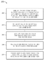
도 2는 본 개시 내용의 하나 이상의 실시예에 따른 오버레이 계측 방법에서 수행되는 단계들을 나타내는 흐름도이다.
도 3a는 본 개시 내용의 하나 이상의 실시예에 따른 적층된 오버레이 타겟 피처들을 포함하는 2-층 오버레이 계측 타겟의 평면도(top view)이다.
도 3b는 본 개시 내용의 하나 이상의 실시예에 따른 적층된 오버레이 타겟 피처들을 포함하는 2-층 오버레이 계측 타겟의 측면도(profile view)이다.
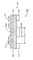
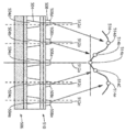
도 4는 본 개시 내용의 하나 이상의 실시예에 따른 입사 입자 빔에 응답하는 오버레이 계측 타겟으로부터의 다수의 방출 소스의 측면도를 포함한다.
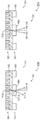
도 5a는 본 개시 내용의 하나 이상의 실시예에 따른 체계적으로 변화하는 공지된 비대칭 오프셋(systematically-varying known asymmetry offsets)을 갖는 교정(calibration) 샘플의 측면도이다.
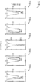
도 5b는 본 개시 내용의 하나 이상의 실시예에 따른 도 5a의 교정 타겟 요소들과 연관된 교정 스캔 신호들을 포함한다. The numerous advantages of the present disclosure may be better understood by those skilled in the art with reference to the accompanying drawings.
1A is a conceptual diagram of an overlay metrology system suitable for device-correlated metrology measurements in accordance with one or more embodiments of the present disclosure.
1B is a conceptual diagram of a particle-based overlay metrology tool according to one or more embodiments of the present disclosure.
2 is a flow diagram illustrating steps performed in an overlay metrology method according to one or more embodiments of the present disclosure.
3A is a top view of a two-layer overlay metrology target comprising stacked overlay target features according to one or more embodiments of the present disclosure.
3B is a profile view of a two-layer overlay metrology target including stacked overlay target features according to one or more embodiments of the present disclosure.
4 includes side views of multiple emission sources from an overlay metrology target responsive to an incident particle beam according to one or more embodiments of the present disclosure.
5A is a side view of a calibration sample with systematically-varying known asymmetry offsets in accordance with one or more embodiments of the present disclosure.
5B includes calibration scan signals associated with calibration target elements of FIG. 5A in accordance with one or more embodiments of the present disclosure.
이제, 첨부된 도면에 예시되는 개시된 발명의 요지에 대해 상세한 참조가 행해질 것이다. 본 개시 내용은 특정 실시예 및 그 특정 피처와 관련하여 특정하게 도시되고 설명되었다. 본원에 설명되는 실시예는 제한적인 것이 아니라 예시적인 것으로 간주된다. 본 개시 내용의 사상 및 범위를 벗어나지 않으면서 형태 및 세부 사항에 대한 다양한 변경 및 수정이 행해질 수 있다는 것이 본 기술 분야의 통상의 기술자에게는 명백하다.Now, detailed reference will be made to the subject matter of the disclosed invention illustrated in the accompanying drawings. The present disclosure has been specifically shown and described with respect to specific embodiments and specific features thereof. The embodiments described herein are considered to be illustrative rather than restrictive. It will be apparent to those skilled in the art that various changes and modifications can be made in form and detail without departing from the spirit and scope of the present disclosure.
본 개시 내용의 실시예들은 2 개의 샘플 층 상에 위치된 적층된 오버레이 타겟 요소들을 가로질러 입자 빔(예컨대, 전자 빔, 이온 빔 등)을 스캐닝함으로써 오버레이를 결정하는 것, 상기 타겟 요소들로부터 대응하는 스캔 신호를 캡처하는 것, 및 상기 스캔 신호의 대칭에 기반하여 상기 오버레이 타겟 요소들의 상대적 포지션을 결정하는 것에 관한 것이다. Embodiments of the present disclosure determine overlay by scanning a particle beam (eg, electron beam, ion beam, etc.) across stacked overlay target elements located on two sample layers, corresponding from the target elements It relates to capturing the scan signal, and determining the relative position of the overlay target elements based on the symmetry of the scan signal.
예를 들어, 스캐닝 전자 현미경(scanning electron microscope)(SEM) 계측 툴(예컨대, 임계 치수(critical dimension) SEM (CD-SEM) 등) 또는 집속 이온 빔(focused ion beam)(FIB) 계측 툴과 같은 하지만 이에 제한되지 않는 입자 빔 계측 툴은 오버레이 타겟의 일부를 가로질러 입자 빔을 스캐닝하고 그 입자 빔에 응답하는 샘플로부터의 방출을 검출할 수 있다. 이러한 방출은 입자 빔에 응답하여 샘플로부터 나오는 다양한 타입의 입자 및/또는 방사선, 예를 들어, 입자 빔의 후방 산란 방출(backscattered emission of the particle beam), 2 차 방출(예컨대, 2 차 전자 방출 등), 또는 전자기 방사선(예컨대, 광)을 포함할 수 있지만, 이에 제한되는 것은 아니다. 또한, 입자 빔은 샘플의 다중 층 상의 타겟 요소들과 상호 작용할 수 있고, 따라서 입자 빔의 에너지에 의해 적어도 부분적으로 결정되는 상호 작용 볼륨에 기반하여 샘플의 다중 층 상의 타겟 요소들을 특성화할 수 있다. 예를 들어, 저에너지 입자 빔은 표면 층을 특성화하는 데 사용될 수 있는 반면, 비교적 고에너지 입자 빔은 샘플 내로 더 깊이 침투하여 이전에 제조된 층 상의 피처들을 특성화할 수 있다. For example, scanning electron microscope (SEM) metrology tools (e.g., critical dimension SEM (CD-SEM), etc.) or focused ion beam (FIB) metrology tools A particle beam metrology tool, but not limited to, can scan a particle beam across a portion of an overlay target and detect emission from a sample responsive to the particle beam. These emissions are various types of particles and/or radiation coming from the sample in response to the particle beam, for example, backscattered emission of the particle beam, secondary emission (e.g. secondary electron emission, etc.) ), or electromagnetic radiation (eg, light), but is not limited thereto. In addition, the particle beam can interact with target elements on multiple layers of a sample, thus characterizing target elements on multiple layers of a sample based on an interaction volume at least partially determined by the energy of the particle beam. For example, a low energy particle beam can be used to characterize a surface layer, while a relatively high energy particle beam can penetrate deeper into a sample to characterize features on previously prepared layers.
반도체 디바이스는 기판 상에 패터닝된 재료의 다중 프린팅 층으로서 형성될 수 있다. 각각의 패터닝된 층은, 하나 이상의 재료 증착 단계, 하나 이상의 리소그래피 단계, 또는 하나 이상의 에칭 단계와 같은 하지만 이에 제한되지 않는 일련의 공정 단계를 통해 제조될 수 있다. 또한, 각각의 패터닝된 층은 전형적으로 최종 디바이스를 적절히 구성하기 위해 특정의 허용 오차 내에서 제조되어야 한다. 예를 들어, 층들 사이의 요소들의 정렬(registration) 또는 그 요소들의 상대적인 배치와 연관된 오버레이와 같은 하지만 이에 제한되지 않는 프린팅 특성은 양호하게 특성화되고 제어되어야 한다. 따라서, 오버레이 타겟은 샘플을 가로질러 다수의 위치에서 하나 이상의 패터닝된 층 상에 제조되어 제조 공정의 효율적인 특성화를 가능하게 할 수 있다. 이와 관련하여, 패터닝된 층 상의 오버레이 타겟 요소들의 프린팅 특성의 편차는 반도체 디바이스의 일부를 형성하는 디바이스 피처를 포함하는 층 상의 모든 요소의 프린팅 특성의 편차를 나타낼 수 있다. 그러나, 샘플 상에서 디바이스 피처들에 대한 오버레이 타겟들의 크기, 배향, 밀도 및/또는 위치의 차이는 타겟에서 측정된 오버레이와 디바이스 피처들의 실제 오버레이 간의 미스매칭을 유발할 수 있다. 따라서, 오버레이 타겟에 대한 디바이스 관련 오버레이 측정을 보장하는 것은 오버레이 계측에서 지속되고 있는 어려운 문제이다. The semiconductor device can be formed as multiple printing layers of patterned material on a substrate. Each patterned layer can be made through a series of process steps such as, but not limited to, one or more material deposition steps, one or more lithography steps, or one or more etching steps. In addition, each patterned layer typically has to be manufactured within certain tolerances to properly configure the final device. Printing characteristics such as, but not limited to, overlays associated with, for example, the alignment of elements between layers or the relative placement of those elements should be well characterized and controlled. Thus, overlay targets can be fabricated on one or more patterned layers at multiple locations across the sample to enable efficient characterization of the manufacturing process. In this regard, variations in printing characteristics of the overlay target elements on the patterned layer may indicate variations in printing characteristics of all elements on the layer including device features that form part of the semiconductor device. However, differences in the size, orientation, density, and/or location of overlay targets relative to device features on the sample can cause mismatching between the overlay measured at the target and the actual overlay of the device features. Therefore, ensuring device-related overlay measurement for an overlay target is a difficult problem that continues to exist in overlay metrology.
본 개시 내용의 실시예는 디바이스 스케일 피처(device-scale features)를 갖는 전용 오버레이 타겟 상에서 오버레이를 측정하는 것에 관한 것이다. 이와 관련하여, 오버레이 타겟의 요소들은 대응하는 디바이스 피처들과 유사한 크기, 형상, 배향, 또는 밀도와 같은 하지만 이에 제한되지는 않는 피처들을 가질 수 있다. 따라서, 관심 대상의 디바이스 구조물들 및 오버레이 타겟은 실질적으로 유사한 특성으로 프린팅될 수 있으며, 이는 타겟 대 디바이스 오차를 완화시킬 수 있다. Embodiments of the present disclosure relate to measuring overlay on a dedicated overlay target with device-scale features. In this regard, elements of the overlay target may have features such as, but not limited to, size, shape, orientation, or density similar to corresponding device features. Thus, the device structures of interest and the overlay target can be printed with substantially similar properties, which can mitigate target-to-device error.
본 개시 내용의 추가 실시예는 관심 대상의 층들 상의 공칭적으로 적층되거나 오버래핑되는 타겟들을 포함하는 오버레이 타겟들 상의 오버레이를 측정하는 것에 관한 것이다. 이와 관련하여, 오버레이 타겟들은 반도체 설계 규칙과 호환되지 않을 수 있는 넓은 개방 영역을 회피할 수 있다. 또한, 적층된 타겟 요소들을 포함하는 오버레이 타겟들은 입자 기반 계측 툴에서 균일한 시야 및 균일한 표면 대전을 가능하게 하여, 빔 배치 왜곡(beam placement distortion) 및 관련 측정 오차를 완화시킬 수 있다. A further embodiment of the present disclosure relates to measuring overlay on overlay targets, including nominally stacked or overlapping targets on layers of interest. In this regard, overlay targets can avoid large open areas that may not be compatible with semiconductor design rules. In addition, overlay targets comprising stacked target elements can enable uniform field of view and uniform surface charging in a particle-based metrology tool, thereby mitigating beam placement distortion and related measurement errors.
예를 들어, 적층된 오버레이 타겟의 오버레이는 관심 대상의 층 상의 타겟 요소들 간의 상대적 포지션에 기반할 수 있다. 또한, 적층된 오버레이 타겟은 공칭 오버레이(nominal overlay)(예를 들어, 샘플 층들 간의 오정렬(misregistration)이 없음)가 관심 대상의 층들 상의 임의의 선택된 타겟 요소 분포에 대응하도록 제조될 수 있다. 예를 들어, 적층된 오버레이 타겟은, 공칭 오버레이가 표면 층 상의 그 타겟 요소들이 표면 아래 층(sub-surface layer) 내의 타겟 바로 위에서 제조되는 타겟 요소들의 대칭 구성(예를 들어, 표면 층 내의 대칭 피처들의 라인들이 표면 아래 층들 내의 대칭 피처들의 라인과 정렬됨)에 대응하도록, 제조될 수 있다. 또 다른 예로서, 적층된 오버레이 타겟은, 공칭 오버레이가 표면 층 상의 타겟 요소들이 표면 아래 층 상의 타겟 요소들에 대해 선택된 비대칭 오프셋으로 제조되는 타겟 요소들의 비대칭 구성에 대응하도록, 제조될 수 있다. For example, the overlay of a stacked overlay target can be based on the relative position between target elements on the layer of interest. In addition, the stacked overlay target can be fabricated such that a nominal overlay (eg, no misregistration between sample layers) corresponds to any selected target element distribution on the layers of interest. For example, a stacked overlay target is a symmetrical configuration of target elements in which a nominal overlay is fabricated directly above the target in a sub-surface layer whose target elements on the surface layer (eg, symmetric features in the surface layer) Lines can be made to correspond to the lines of symmetric features in the layers below the surface). As another example, a stacked overlay target can be manufactured such that the nominal overlay corresponds to an asymmetric configuration of target elements where the target elements on the surface layer are manufactured with an asymmetric offset selected for the target elements on the layer below the surface.
본원에서 인식되는 것은, 적층된 오버레이 타겟 요소들과의 입자 빔 상호 작용과 연관된 샘플 방출이 샘플의 다중 층들 상의 타겟 요소들과 연관된 다수의 방출 소스를 포함할 수 있다는 것이다. 예를 들어, 적층된 오버레이 타겟 피처들과 상호 작용하는 전자 빔은 다중 샘플 층 상의 타겟 요소들로부터 후방 산란 방출 및 2 차 방출을 동시에 유도할 수 있으며, 그에 따라 검출된 방출 소스를 구별하는 것이 어려울 수 있다. 본 개시 내용의 추가 실시예는 하나 이상의 적층된 오버레이 타겟 요소들을 가로 지르는 스캔 신호의 대칭에 기반하여 오버레이를 검출하는 것에 관한 것이다. 예를 들어, 다중 층을 가로 지르는 대칭 정렬 타겟 구조물의 방출 신호는 또한 대칭일 수 있다. 반대로, 비대칭 정렬 타겟 구조물의 방출 신호는 비대칭일 수 있다. 따라서, 스캔 신호의 대칭은 하부의 대칭 피처들의 측정치 및 그에 따른 오버레이를 결정하기에 적합한 타겟 피처들의 상대적 포지션의 측정치를 제공할 수 있다. What is recognized herein is that sample emission associated with particle beam interactions with stacked overlay target elements can include multiple emission sources associated with target elements on multiple layers of a sample. For example, an electron beam interacting with stacked overlay target features can simultaneously induce backscattered emission and secondary emission from target elements on multiple sample layers, thus making it difficult to distinguish the detected emission source. Can. A further embodiment of the present disclosure is directed to detecting overlays based on symmetry of the scan signal across one or more stacked overlay target elements. For example, the emission signal of a symmetrically aligned target structure across multiple layers can also be symmetrical. Conversely, the emission signal of the asymmetric alignment target structure may be asymmetric. Thus, the symmetry of the scan signal can provide a measure of the underlying symmetric features and thus a relative measure of the target features suitable for determining the overlay.
본 개시 내용의 추가 실시예는 하나 이상의 대칭 메트릭에 기반하여 다중 층들 상의 오버레이의 값(예를 들어, 오버레이 타겟 구조물 간의 오정렬의 값)을 추출하는 것에 관한 것이다. 예를 들어, 대칭 메트릭은 스캔 신호에서의 다수의 피크, 스캔 신호에서의 피크들의 값, 오버레이 타겟 구조물의 중심에 대한 스캔 신호의 피크들의 위치, 스캔 신호 피크들의 분리 거리, 또는 스캔 신호의 적분을 포함할 수 있지만, 이에 제한되는 것은 아니다. 추가 실시예는 대칭 메트릭을 오버레이 값과 상관시키는 것에 관한 것이다. 예를 들어, 공지된 비대칭 오프셋들과 함께 다중 층들 상의 오버레이 타겟 피처들을 갖는 교정(calibration) 오버레이 타겟에 대해 교정 스캔 신호들이 생성될 수 있다. 이어서, 교정 스캔 신호들 및 대응하는 공지된 비대칭 오프셋들은 스캔 신호들의 대칭 특성들과 오버레이 측정치들 사이의 상관 관계를 생성하는 데 사용될 수 있고, 그에 따라 상관 관계에 기반하여 임의의 스캔 신호로부터 오버레이 측정치가 추출될 수 있다. 또한, 상관 관계는 패턴 인식 기술, 주요 성분 분석, 또는 머신 러닝 기술과 같은 하지만 이에 제한되지 않는 본 기술 분야에서 공지된 임의의 방법을 사용하여 생성될 수 있다. A further embodiment of the present disclosure relates to extracting the value of overlay on multiple layers (eg, the value of misalignment between overlay target structures) based on one or more symmetric metrics. For example, the symmetry metric can be used to determine the number of peaks in the scan signal, the values of the peaks in the scan signal, the position of the peaks of the scan signal relative to the center of the overlay target structure, the separation distance of the scan signal peaks, or the integral of the scan signal. May include, but is not limited to. A further embodiment relates to correlating symmetric metrics with overlay values. For example, calibration scan signals can be generated for a calibration overlay target with overlay target features on multiple layers with known asymmetric offsets. Subsequently, the calibration scan signals and corresponding known asymmetric offsets can be used to generate a correlation between the symmetric properties of the scan signals and the overlay measurements, thus overlay measurements from any scan signal based on the correlation. Can be extracted. Further, the correlation can be generated using any method known in the art, such as, but not limited to, pattern recognition technology, principal component analysis, or machine learning technology.
본 개시 내용의 추가 실시예는 오버레이 측정치에 기반하여 오버레이 보정 가능한 것을 생성하는 것에 관한 것이다. 오버레이 보정 가능한 것은 그 후 피드백 및/또는 피드포워드 데이터로서 제조 툴(예를 들어, 리소그래피 툴)에 제공될 수 있다. 예를 들어, 샘플 상에서 측정된 현재 공정 단계와 연관된 오버레이 측정치는, 동일 또는 후속 로트들에서 후속 샘플에 대한 처리 단계에 대한 드리프트를 보상하고 오버레이를 선택된 허용 오차 내로 유지하는 데 사용될 수 있다. 다른 예로서, 현재의 공정 단계와 연관된 오버레이 측정치는 후속 공정 단계를 조정하도록 피드포워드되어 임의의 측정된 오버레이 오차를 보상할 수 있다. Additional embodiments of the present disclosure relate to creating overlay correctables based on overlay measurements. The overlay correctable can then be provided to manufacturing tools (eg, lithography tools) as feedback and/or feedforward data. For example, an overlay measurement associated with the current process step measured on a sample can be used to compensate for drift for a processing step for a subsequent sample in the same or subsequent lots and keep the overlay within a selected tolerance. As another example, overlay measurements associated with a current process step can be fed forward to adjust subsequent process steps to compensate for any measured overlay error.
도 1a는 본 개시 내용의 하나 이상의 실시예에 따른 디바이스 상관 계측 측정(device-correlated metrology measurements)에 적합한 오버레이 계측 시스템(100)의 개념도이다. 일 실시예에서, 오버레이 계측 시스템(100)은 적층된 오버레이 타겟 피처들의 층간 오버레이 측정뿐만 아니라 층내 패턴 배치 거리를 측정하는 데 적합한 적어도 하나의 오버레이 계측 툴(102)을 포함한다. 1A is a conceptual diagram of an
다른 실시예에서, 오버레이 계측 시스템(100)은 컨트롤러(104)를 포함한다. 다른 실시예에서, 컨트롤러(104)는 메모리 매체(108) 상에 유지되는 프로그램 명령어를 실행하도록 구성된 하나 이상의 프로세서(106)를 포함한다. 이와 관련하여, 컨트롤러(104)의 하나 이상의 프로세서(106)는 본 개시 내용의 전체에 걸쳐 설명되는 다양한 공정 단계 중 임의의 것을 실행할 수 있다. 예를 들어, 컨트롤러(104)는 오버레이 계측 툴(102)로부터 데이터를 수신할 수 있고, 디바이스 상관 오버레이 데이터를 추가로 생성할 수 있다. 다른 예로서, 컨트롤러(104)는 오버레이 계측 툴(102)로부터의 데이터에 기반하여 디바이스 관련 오버레이 보정 가능한 것을 생성할 수 있다. In another embodiment, the
또한, 컨트롤러(104)는 리소그래피 툴과 같은 하지만 이에 제한되지는 않는 하나 이상의 외부 제조 툴에 통신 가능하게 연결될 수 있다. 이와 관련하여, 컨트롤러(104)는 오버레이를 선택된 오버레이 허용 오차 내로 유지하기 위해 외부 제조 툴의 입력을 제어하기에 적합한 고급 공정 컨트롤러(advanced process controller)(APC)로서 동작할 수 있다. Further, the
컨트롤러(104)의 하나 이상의 프로세서(106)는 본 기술 분야에서 공지된 임의의 프로세싱 요소를 포함할 수 있다. 이러한 의미에서, 하나 이상의 프로세서(106)는 알고리즘 및/또는 명령어를 실행하도록 구성된 임의의 마이크로프로세서 타입의 디바이스를 포함할 수 있다. 일 실시예에서, 하나 이상의 프로세서(106)는 본 개시 내용의 전체에 걸쳐 설명되는 바와 같이, 오버레이 계측 시스템(100)을 동작시키도록 구성된 프로그램을 실행하도록 구성된 데스크탑 컴퓨터, 메인프레임 컴퓨터 시스템, 워크스테이션, 이미지 컴퓨터, 병렬 프로세서, 또는 임의의 다른 컴퓨터 시스템(예컨대, 네트워크형 컴퓨터)을 구성할 수 있다. 추가로 인식되는 것은, 용어 "프로세서"는 비일시적인 메모리 매체(108)로부터의 프로그램 명령어를 실행하는 하나 이상의 프로세싱 요소를 갖는 임의의 디바이스를 포괄하도록 광범위하게 정의될 수 있다는 것이다. 또한, 본 개시 내용의 전체에 걸쳐 설명되는 단계들은 단일 컨트롤러(104) 또는 대안적으로 다수의 컨트롤러에 의해 수행될 수 있다. 추가적으로, 컨트롤러(104)는 하나의 공통 하우징 내에 또는 다수의 하우징 내에 하우징되는 하나 이상의 컨트롤러를 포함할 수 있다. 이러한 방식으로, 임의의 컨트롤러 또는 컨트롤러들의 조합은 오버레이 계측 시스템(100) 내로의 통합에 적합한 모듈로서 개별적으로 패키징될 수 있다. One or more processors 106 of
메모리 매체(108)는 관련된 하나 이상의 프로세서(106)에 의해 실행 가능한 프로그램 명령어를 저장하기에 적합한 본 기술 분야에서 공지된 임의의 저장 매체를 포함할 수 있다. 예를 들어, 메모리 매체(108)는 비일시적인 메모리 매체를 포함할 수 있다. 다른 예로서, 메모리 매체(108)는 판독 전용 메모리, 랜덤 액세스 메모리, 자기 또는 광학 메모리 디바이스(예를 들어, 디스크), 자기 테이프, 고체 상태 드라이브(solid state drive)(SSD) 등을 포함할 수 있지만, 이에 제한되지는 않는다. 추가로 주목되는 것은 메모리 매체(108)가 하나 이상의 프로세서(106)와 함께 공통 컨트롤러 하우징 내에 하우징될 수 있다는 것이다. 일 실시예에서, 메모리 매체(108)는 하나 이상의 프로세서(106) 및 컨트롤러(104)의 물리적 위치에 대해 원격에 위치될 수 있다. 예를 들어, 컨트롤러(104)의 하나 이상의 프로세서(106)는 네트워크(예컨대, 인터넷, 인트라넷 등)를 통해 액세스 가능한 원격 메모리(예컨대, 서버)에 액세스할 수 있다. 그러므로, 전술한 설명은 본 발명에 대한 제한으로서 해석되어서는 안되며 단지 예시에 불과할 뿐이다.
다른 예로서, 오버레이 계측 툴(102)은 샘플을 가로질러 집속된 빔을 스캐닝하고 하나 이상의 검출기 상의 샘플로부터 하나 이상의 측정 각도로 나오는 방사선 및/또는 입자를 캡처하여 이미지를 생성할 수 있다. 집속된 빔은 빔 경로를 (예를 들어, 갈보 미러(galvo mirror), 압전 미러(piezo-electric mirror) 등을 사용하여) 수정함으로써 및/또는 집속된 빔의 초점 볼륨(focal volume)을 통해 샘플을 병진시킴으로써 샘플을 가로질러 스캐닝될 수 있다.As another example, the
도 1b는 본 개시 내용의 하나 이상의 실시예에 따른 입자 기반 오버레이 계측 툴(102)의 개념도이다. 오버레이 계측 툴(102)은 디바이스 피처들 또는 디바이스 스케일 피처들을 분해하기에 적합한 임의의 타입의 계측 툴, 예를 들어, 전자 빔 계측 툴(예컨대, SEM, CD-SEM 등), 또는 이온 빔 계측 툴(예컨대, 집속 이온 빔(focused-ion-beam)(FIB) 계측 툴)을 포함할 수 있지만, 이에 제한되지는 않는다. 1B is a conceptual diagram of a particle-based
일 실시예에서, 오버레이 계측 툴(102)은 입자 빔(112)(예컨대, 전자 빔, 입자 빔 등)을 생성하기 위한 입자 소스(110)(예컨대, 전자 빔 소스, 이온 빔 소스 등)를 포함한다. 입자 소스(110)는 입자 빔(112)을 생성하기에 적합한 본 기술 분야에서 공지된 임의의 입자 소스를 포함할 수 있다. 예를 들어, 입자 소스(110)는 전자 건(electron gun) 또는 이온 건(ion gun)을 포함할 수 있지만, 이에 제한되지는 않는다. 다른 실시예에서, 입자 소스(110)는 조정 가능한 에너지(tunable energy)를 갖는 입자 빔을 제공하도록 구성된다. 예를 들어, 전자 소스를 포함하지만 이에 제한되지는 않는 입자 소스(110)는 0.1 kV 내지 30 kV의 범위의 가속 전압을 제공할 수 있다. 다른 예로서, 이온 소스를 포함하는 입자 소스(110)는 1 내지 50 keV의 범위의 에너지를 갖는 이온 빔을 제공할 수 있지만, 이를 제공할 필요는 없다. In one embodiment, the
다른 실시예에서, 오버레이 계측 툴(102)은 하나 이상의 입자 집속 요소(114)를 포함한다. 예를 들어, 하나 이상의 입자 집속 요소(114)는 단일 입자 집속 요소 또는 복합 시스템(compound system)을 형성하는 하나 이상의 입자 집속 요소를 포함할 수 있지만, 이에 제한되지는 않는다. 다른 실시예에서, 하나 이상의 입자 집속 요소(114)는 입자 빔(112)을 샘플 스테이지(120) 상에 위치한 샘플(118)로 지향시키도록 구성된 입자 대물 렌즈(116)를 포함한다. 또한, 하나 이상의 입자 소스(110)는 정전기, 자기, 단 전위(uni-potential) 또는 이중 전위(double-potential) 렌즈를 포함하지만 이에 제한되지는 않는 본 기술 분야에서 공지된 임의의 타입의 전자 렌즈(electron lenses)를 포함할 수 있다. In other embodiments, the
다른 실시예에서, 오버레이 계측 툴(102)은 샘플(118)로부터 나오는 입자를 이미지화하거나 다른 방식으로 검출하기 위한 하나 이상의 검출기(122)를 포함한다. 일 실시예에서, 검출기(122)는 전자 컬렉터(electron collector)(예컨대, 2 차 전자 컬렉터, 후방 산란 전자 검출기 등)를 포함한다. 다른 실시예에서, 검출기(122)는 샘플(118)로부터 전자 및/또는 광자를 검출하기 위한 광자 검출기(예컨대, 광 검출기, x-선 검출기, 광전자 증배관(photomultiplier tube)(PMT) 검출기에 연결된 신틸레이팅 요소(scintillating element) 등)를 포함한다. In other embodiments, the
다른 실시예에서, 도시되지는 않았지만, 오버레이 계측 툴(102)은 샘플(118)로부터의 방출을 캡처하여 이를 하나 이상의 검출기(122)로 지향시키는 하나 이상의 수집 렌즈(collection lenses)를 포함한다. 예를 들어, 대물 렌즈(116)는 샘플로부터 방출을 수집하기 위한 수집 렌즈로서 동작할 수 있다. 또한, 하나 이상의 수집 요소(예컨대, 하나 이상의 추가 렌즈, 빔 편향기 등)는 방출을 하나 이상의 검출기(122)로 지향시킬 수 있다.In other embodiments, although not shown, the
이해되어야 하는 것은, 도 1b에 도시된 바와 같은 오버레이 계측 툴(102)의 설명 및 관련된 전술한 설명은 단지 예시 목적으로만 제공되며 제한하는 것으로 해석되어서는 안된다는 것이다. 예를 들어, 오버레이 계측 툴(102)은 샘플(118)을 동시에 조사(interrogating)하기에 적합한 다중 빔 및/또는 다중 열 시스템(multi-beam and/or a multi-column system)을 포함할 수 있다. 추가 실시예에서, 오버레이 계측 툴(102)은 샘플(108)의 하나 이상의 위치에 하나 이상의 전압을 인가하도록 구성된 하나 이상의 컴포넌트(예를 들어, 하나 이상의 전극)를 포함할 수 있다. 이와 관련하여, 오버레이 계측 툴(102)은 전압 콘트라스트 이미징 데이터(voltage contrast imaging data)를 생성할 수 있다.It should be understood that the description of the
본원에서 인식되는 것은, 샘플(118)에서 입자 빔(112)의 침투 깊이는 입자 에너지에 의존할 수 있으며, 그에 따라 더 높은 에너지 빔은 전형적으로 샘플 내로 더 깊이 침투할 수 있게 된다는 것이다. 일 실시예에서, 오버레이 계측 툴(102)은 샘플(118) 내로의 입자 빔(112)의 침투 깊이에 기반하여 디바이스의 상이한 층들을 조사하기 위한 상이한 입자 에너지를 이용한다. 예를 들어, 오버레이 계측 툴(102)은 비교적 저에너지 전자 빔(예컨대, 약 1 keV 이하)을 이용할 수 있고, 이전에 제조된 층을 특성화하기 위해 보다 높은 에너지 빔(예컨대, 약 10 keV 이상)을 이용할 수 있다. 본원에서 인식되는 것은, 입자 에너지의 함수로서의 침투 깊이는 재료마다 다를 수 있으며, 그에 따라 특정 층에 대한 입자 에너지의 선택은 재료마다 다를 수 있다는 것이다. What is recognized herein is that the depth of penetration of the
도 2는 본 개시 내용의 하나 이상의 실시예에 따른 오버레이 계측 방법(200)에서 수행되는 단계들을 나타내는 흐름도이다. 본 출원인이 주목하는 것은 오버레이 계측 시스템(100)의 맥락에서 전술한 실시예 및 가능한 기술이 방법(200)으로 확장되도록 해석되어야 한다는 것이다. 그러나, 방법(200)은 오버레이 계측 시스템(100)의 아키텍처에 제한되지는 않는다는 것이 또한 주목된다. 2 is a flow diagram illustrating steps performed in an
일 실시예에서, 방법(200)은 샘플 상의 오버레이 타겟을 가로질러 입자 빔을 스캐닝하는 단계(202)를 포함하며, 상기 오버레이 타겟은 상기 샘플의 제 1 층 상의 제 1 층 타겟 요소 및 상기 제 1 층에 후속해서 제조되는 상기 샘플의 제 2 층 상의 제 2 층 타겟 요소를 포함한다. In one embodiment,
도 3a 및 도 3b는 본 개시 내용의 하나 이상의 실시예에 따른 적층된 오버레이 타겟 피처들을 갖는 오버레이 타겟을 도시하고 있다. 구체적으로, 도 3a는 본 개시 내용의 하나 이상의 실시예에 따른 적층된 오버레이 타겟 피처들을 포함하는 2-층 오버레이 계측 타겟(302)의 평면도이다. 또한, 도 3b는 본 개시 내용의 하나 이상의 실시예에 따른 적층된 오버레이 타겟 피처들을 포함하는 2-층 오버레이 계측 타겟(302)의 측면도이다. 일 실시예에서, 오버레이 계측 타겟(302)은 샘플(118)의 제 1 층(306) 상의 제 1 층 타겟 요소(304)를 포함하고 샘플(118)의 제 2 층(310) 상의 제 2 층 타겟 요소(308)를 추가로 포함한다. 예를 들어, 제 2 층(310)은 제 1 층(306)에 후속해서 제조될 수 있고 현재 제조 층을 나타낼 수 있다. 후속 제조 단계에서 제 2 층 타겟 요소(308) 상에 하나 이상의 추가 층이 제조될 수 있는 경우가 있을 수 있다. 3A and 3B show an overlay target with stacked overlay target features according to one or more embodiments of the present disclosure. Specifically, FIG. 3A is a top view of a two-layer
오버레이 타겟의 주어진 층 상의 타겟 요소들은 샘플의 2 개 이상의 층 간의 오버레이를 측정하기에 적합한 임의의 크기, 형상, 배향, 또는 분포를 가질 수 있다. 예를 들어, 도 3a 및 도 3b에 도시된 바와 같이, 제 1 층 타겟 요소들(304)은 제 1 층 피치(312)로 주기적으로 분포될 수 있고, 제 2 층 타겟 요소들(308)은 제 2 층 피치(314)로 분포될 수 있다. 또한, 제 1 층 타겟 요소들(304)은 제 1 층 요소 폭(316)을 가질 수 있는 반면, 제 2 층 타겟 요소들(308)은 제 2 층 요소 폭(318)을 가질 수 있다. 또한, 상이한 층들 상의 타겟 피처들의 주기 및/또는 폭은 동일하거나 상이할 수 있다. 예를 들어, 도 3a 및 도 3b에 도시된 바와 같이, 제 2 층 피치(314)는 제 1 층 피치(312)보다 3 배 더 크다. 추가적으로, 제 2 층 요소 폭(318)은 각각의 제 2 층 타겟 요소(308)가 3 개의 제 1 층 타겟 요소(304)와 중첩되도록 제 1 층 요소 폭(316)보다 3 배 더 크다. Target elements on a given layer of an overlay target can have any size, shape, orientation, or distribution suitable for measuring an overlay between two or more layers of a sample. For example, as shown in FIGS. 3A and 3B, the first
일 실시예에서, 오버레이 타겟의 하나 이상의 층 상의 타겟 피처들은 대응하는 층들 상의 디바이스 피처들을 나타내는 크기, 형상, 배향, 또는 분포를 가질 수 있다. 이와 관련하여, 오버레이 타겟 피처들은 대응하는 디바이스 피처들과 실질적으로 동일한 특성들(예컨대, 패턴 배치 오차, 측벽 각도, 임계 치수 등)로 제조될 수 있고, 그에 따라, 오버레이 타겟 상에서 측정된 오버레이는 샘플 상의 대응하는 디바이스 피처들의 오버레이를 정확하게 나타낼 수 있게 된다. 예를 들어, 타겟 피처 피치(target feature pitch)(예컨대, 제 1 층 피치(312), 제 2 층 피치(314) 등) 및/또는 타겟 피처 폭(target feature width)(예컨대, 제 1 층 요소 폭(316), 제 2 층 요소 폭(318) 등)은 디바이스 피처들을 나타낼 수 있다. 본원에서 인식되는 것은, 샘플의 주어진 층 상의 디바이스 피처들이 다양한 크기, 형상, 배향, 또는 분포를 가질 수 있다는 것이다. 따라서, 디바이스 스케일 오버레이 타겟 요소는 관심 대상의 디바이스 피처들 중 적어도 일부를 나타내는 치수를 가질 수 있다. In one embodiment, target features on one or more layers of the overlay target may have a size, shape, orientation, or distribution that represents device features on corresponding layers. In this regard, overlay target features can be manufactured with substantially the same characteristics as corresponding device features (eg, pattern placement error, sidewall angle, critical dimension, etc.), whereby the overlay measured on the overlay target is sampled. It is possible to accurately represent an overlay of corresponding device features on the image. For example, target feature pitch (e.g.,
주어진 층 상의 타겟 요소들은 샘플의 둘 이상의 층 간의 오버레이를 결정하기에 적합한 임의의 구성으로 적층될 수 있다. 일 실시예에서, 인접한 샘플 층들 상의 적어도 일부의 타겟 요소들은 공칭 대칭 구성으로 제조된다. 이와 관련하여, 샘플 층들 간의 오버레이는 대칭의 중단에 기반하여(예컨대, 비대칭 제조에 의해) 식별될 수 있다. Target elements on a given layer can be stacked in any configuration suitable for determining an overlay between two or more layers of a sample. In one embodiment, at least some of the target elements on adjacent sample layers are fabricated in a nominally symmetrical configuration. In this regard, overlays between sample layers can be identified based on disruption of symmetry (eg, by asymmetric manufacturing).
예를 들어, 도 3b의 측면도에 도시된 바와 같이, 제 2 층 타겟 요소(308a)는 제 1 층 타겟 요소(304a) 바로 위에 (및 제 1 층 타겟 요소들(304a 내지 304c)의 그룹 위에 대칭적으로) 제 1 층(306)과 제 2 층(310) 간의 제로 오정렬과 연관된 공칭 오버레이를 나타낼 수 있지만, 이를 나타낼 필요는 없는 대칭 구성으로 제조될 수 있다. 따라서, 타겟 피처들의 분리 방향(예컨대, 도 3a 및 도 3b에서의 X-방향)을 따라 제 1 층(306)과 제 2 층(310) 간의 오정렬은 제 1 층 타겟 요소들(304)에 대한 제 2 층 타겟 요소들(308)의 대칭의 중단으로 나타날 수 있다. 또한, 제 1 층 타겟 요소들(304)에 대한 제 2 층 타겟 요소들(308)의 대칭의 중단은 대칭 구성에 대한 제 2 층 타겟 요소들(308) 간의 오정렬의 값을 나타내는 비대칭 오프셋에 의해 특성화될 수 있다.For example, as shown in the side view of FIG. 3B, the second
그러나, 도 3a 및 도 3b에 도시된 오버레이 계측 타겟(302)은 관련 설명과 함께, 단지 예시적인 목적으로만 제공되며 제한적인 것으로 해석되어서는 안된다는 것을 이해해야 한다. 예를 들어, 오버레이 타겟은 하나 이상의 층 내의 단일 타겟 요소를 가질 수 있으며, 그에 따라 오버레이 측정을 위해 인접한 관심 대상의 층들 상의 타겟 요소들은 적층될 수 있게 된다. 다른 예로서, 제 2 층 요소 폭(318)은 제 1 층 요소 폭(316)보다 작을 수 있으며, 그에 따라 제 1 층 타겟 요소(304)의 일부가 평면도에서 보여질 수 있다. 다른 예로서, 제 2 층 피치(314)는 제 1 층 피치(312)와 같거나 작을 수 있다. 다른 예로서, 주어진 층 상의 오버레이 타겟 피처들은 관심 대상 층들 간의 대칭이 유지되는 한, 다양한 크기, 형상, 배향, 및/또는 분포를 가질 수 있다. However, it should be understood that the
단계(202)는 오버레이 타겟(예컨대, 오버레이 계측 타겟(302))을 가로질러 임의의 타입의 입자 빔을 스캐닝하는 단계를 포함할 수 있다. 예를 들어, 입자 빔은 입자 기반 오버레이 계측 툴(102)을 사용하여 생성될 수 있지만 입자 기반 오버레이 계측 툴(102)을 사용하여 생성되도록 요구되는 것은 아니다. 따라서, 입자 빔(예컨대, 입자 빔(112) 등)은 전자 빔, 이온 빔(예컨대, 양성자 빔 등), 또는 중성 입자의 빔을 포함할 수 있지만 이에 제한되지는 않는다. Step 202 can include scanning any type of particle beam across an overlay target (eg, overlay metrology target 302). For example, a particle beam may be generated using a particle based
또한, 단계(202)는 입자 빔이 관심 대상의 다중 층들 상의 타겟 요소들과 상호 작용하도록 입자 빔을 오버레이 타겟의 하나 이상의 타겟 요소에 대해 스캐닝하는 단계를 포함할 수 있다. 본원에서 전술한 바와 같이, 입자 빔(예컨대, 입자 빔(112) 등)의 상호 작용 볼륨 및/또는 상호 작용 깊이는 적어도 빔 에너지의 함수일 수 있으며, 입자 빔의 침투 깊이는 빔 에너지에 따라 증가하게 된다.In addition,
예를 들어, 다시 도 3a 및 도 3b를 참조하면, 단계(202)는 제 1 층 타겟 요소들(304a 내지 304c)과 상호 작용하기에 충분한 빔 에너지로 적어도 제 2 층 타겟 피처(304a)에 대해 입자 빔을 스캐닝하는 단계를 포함할 수 있다. For example, referring back to FIGS. 3A and 3B,
다른 실시예에서, 방법(200)은 제 1 층 타겟 요소 및 제 2 층 타겟 요소 모두와의 입자 빔의 상호 작용과 연관된 스캔 신호를 캡처하는 단계(204)를 포함한다. 예를 들어, 단계(204)는 단계(202)에서 스캐닝된 입자 빔에 응답하여 샘플로부터 검출된 방출과 연관된 스캔 신호를 캡처하는 단계를 포함할 수 있다. 또한, 스캔 신호는 입자 빔으로 샘플을 스캐닝하는 것에 응답하여 생성된 다수의 타입의 방출, 예를 들어, 하지만 이에 제한되는 것은 아닌, 입자 빔의 후방 산란 방출(backscattered emission)(BSE) 또는 입자의 2 차 방출(secondary emission)(SE) 및/또는 전자기 방사선(예컨대, 광)에 기반하여 생성될 수 있다. In another embodiment, the
도 4는 본 개시 내용의 하나 이상의 실시예에 따른 입사 입자 빔(112)에 응답하는 오버레이 계측 타겟(302)으로부터의 다수의 방출 소스의 측면도를 포함한다. 측면도(402)는 샘플에서 입자 빔(112)의 반사와 연관된(예컨대, 입자 빔(112)의 탄성 산란과 연관된) 후방 산란 방출의 일부 가능한 소스를 도시하고, 측면도(404)는 샘플(118)에서 입자 빔(112)의 흡수에 의해 유도되는 2 차 방출의 일부 가능한 소스를 도시한다. 4 includes side views of multiple emission sources from an
일 실시예에서, 입자 빔(112)은 전자 빔(예컨대, 스캐닝 전자 현미경 계측 시스템에 의해 생성됨)을 포함한다. 입자 빔(112)과의 상호 작용은 그 후 샘플로부터 다수의 방출 신호를 생성할 수 있다. 예를 들어, 입자 빔(112)은 제 2 층 타겟 요소(308a)와의 상호 작용에 기반하여 제 2 층 BSE(406)를 생성 및/또는 제 2 층(310)을 통과한 후 제 1 층 타겟 요소(304a)와의 상호 작용에 기반하여 제 1 층 BSE(408)를 생성할 수 있다. 다른 예로서, 입자 빔(112)은 다수의 소스로부터 2 차 전자(secondary electrons)(SE)의 생성을 유도할 수 있다. 예를 들어, 입자 빔(112)은 제 2 층 타겟 요소(308a)로부터 제 2 층 SE(410)를 생성할 수 있다. 다른 예에서, 입자 빔(112)은 제 2 층(310)을 통과한 후 제 1 층 타겟 요소(304a)로부터 제 1 층 SE(412)를 생성할 수 있다. 다른 예에서, 도 4에 도시된 바와 같이, 제 1 층(306)에서 생성된 제 1 층 BSE(408)의 일부의 흡수시 제 2 층(310)에서 추가의 제 2 층 SE(414)가 생성되어 표면을 향해 다시 전파될 수 있다. In one embodiment,
입자 빔(112)에 응답하여 생성된 방출은 단계(202)에서 관심 대상의 방출을 캡처하기에 적합한 임의의 개수의 검출기에 의해 캡처될 수 있다. 예를 들어, 방출은 오버레이 계측 시스템(100)의 적어도 하나의 검출기(122)에 의해 캡처될 수 있다. 또한, 임의의 검출기(122)는 스캔 동안 샘플을 가로 지르는 입자 빔(112)의 포지션의 함수로서 캡처된 신호의 강도와 연관된 스캔 신호를 생성할 수 있다. Emissions generated in response to
다른 실시예에서, 방법(200)은 상기 스캔 신호에 대해 하나 이상의 대칭 메트릭과 관련한 하나 이상의 대칭 측정치를 결정하는 단계(206)를 포함한다. 다른 실시예에서, 방법(200)은 하나 이상의 대칭 측정치에 기반하여 제 1 층과 제 2 층 간의 오버레이 측정치를 생성하는 단계(208)를 포함하며, 여기서 스캔 신호의 비대칭은 제 1 층 타겟 요소에 대한 제 2 층 타겟 요소의 오정렬을 나타내며, 오버레이 측정치의 값은 하나 이상의 대칭 측정치에 기반하고 있다. 스캔 신호에 대한 하나 이상의 대칭 측정치를 결정하는 단계(206) 및/또는 단계(208)는 오버레이 계측 시스템(100)의 컨트롤러(104)를 사용하여 수행될 수 있지만, 오버레이 계측 시스템(100)의 컨트롤러(104)를 사용하여 수행될 필요는 없다. 예를 들어, 컨트롤러(104)는 스캔 신호를 수신하기 위해 검출기(122)에 통신 가능하게 연결될 수 있고, 스캔 신호의 대칭을 분석하기 위해 스캔 신호를 추가로 분석하고 대칭 측정치에 기반하여 오버레이 측정치를 추가로 생성할 수 있다. In another embodiment,
본원에서 인식되는 것은, 검출기(예컨대, 검출기(122))는 샘플로부터 다수의 방출 소스(예컨대, 제 1 층 BSE(408), 제 2 층 BSE(406), 제 1 층 SE(412), 제 2 층 SE(410), 및/또는 추가의 제 2 층 SE(414)의 임의의 조합)를 동시에 캡처할 수 있다는 것이다. 그러나, 임의의 조합의 방출 소스를 포함하는 스캔 신호의 대칭 또는 비대칭은 입자 빔에 의해 스캐닝된 샘플 피처들의 기본 대칭 또는 비대칭을 반영할 수 있는 경우가 있을 수 있다. 따라서, 단계(206)는 임의의 개수의 대칭 메트릭과 관련한 대칭 측정치를 결정함으로써 스캔 신호를 특성화할 수 있다. 또한, 단계(208)는 대칭 측정치에 기반하여 오버레이 측정치를 결정할 수 있다. As recognized herein, detectors (e.g., detectors 122) include multiple emission sources from a sample (e.g.,
예를 들어, 넌제로(non-zero) 오버레이(예컨대, 샘플 층들의 오정렬)의 존재는 공칭 대칭 측정치로부터 스캔 신호의 대칭 측정치의 편차에 기반하여 식별될 수 있다. 예를 들어, 넌제로 오버레이는 오버레이 타겟 요소들의 대칭 구성 또는 선택된 비대칭 오프셋과 연관된 선택된 비대칭 구성에 대응할 수 있다. 또한, 샘플 층들 간의 오정렬의 크기 및/또는 방향을 포함하는 오버레이 측정 값이 하나 이상의 대칭 메트릭과 관련한 스캔 신호의 분석에 기반하여 생성될 수 있다. For example, the presence of a non-zero overlay (eg, misalignment of sample layers) can be identified based on the deviation of the symmetric measurement of the scan signal from the nominal symmetric measurement. For example, the non-zero overlay can correspond to a symmetric configuration of overlay target elements or a selected asymmetric configuration associated with a selected asymmetric offset. In addition, overlay measurements, including the magnitude and/or direction of misalignment between sample layers, can be generated based on analysis of scan signals related to one or more symmetric metrics.
일 실시예에서, 공지된 비대칭 오프셋(예컨대, 대칭 구성으로부터 관심 대상의 샘플 층들 상의 타겟 피처들의 공지된 편차)과 대응하는 스캔 신호 간의 매핑을 제공하는 교정 데이터 세트와 관련한 오버레이 측정 값이 생성될 수 있다. 예를 들어, 하나 이상의 교정 샘플은 관심 대상의 샘플 층들 간의 체계적으로 변화하는 비대칭 오프셋으로 배열되는 측정 대상의 오버레이 타겟(예컨대, 오버레이 계측 타겟(302) 등)에 대응하는 적층된 오버레이 타겟 요소로 제조될 수 있다. 또한, 각각의 공지된 비대칭 오프셋과 연관된 교정 스캔 신호는 오버레이 계측 툴(예컨대, 오버레이 계측 툴(102))로 생성될 수 있다. 따라서, 교정 스캔 신호와 연관된 대칭 측정치가 분석되어 대칭 측정치와 공지된 비대칭 오프셋 간의 매핑을 생성할 수 있다. 따라서, 교정 데이터 세트는 임의의 관심 대상의 샘플 상에서 측정된 스캔 신호를 비대칭 오프셋에 매핑하는 데 사용될 수 있다. In one embodiment, overlay measurements associated with a set of calibration data that provide a mapping between a known asymmetric offset (eg, a known deviation of target features on sample layers of interest from a symmetric configuration) and a corresponding scan signal can be generated. have. For example, one or more calibration samples are made of a stacked overlay target element corresponding to an overlay target of a measurement object (e.g.,
비대칭 오프셋은 그 후 오버레이 값과 상관될 수 있다. 예를 들어, 대응하는 타겟 피처들의 비대칭 오프셋들의 편차에 대한 스캔 신호의 감도는 오프셋마다 다를 수 있다. 따라서, 오버레이 타겟은 관심 대상의 샘플 층들 상의 타겟 피처들 간의 임의의 선택된 비대칭 오프셋으로 제조되어 원하는 감도를 제공할 수 있다.The asymmetric offset can then be correlated with the overlay value. For example, the sensitivity of the scan signal to the deviation of asymmetric offsets of corresponding target features may vary from offset to offset. Thus, the overlay target can be made with any selected asymmetric offset between target features on sample layers of interest to provide the desired sensitivity.
도 5a는 본 개시 내용의 하나 이상의 실시예에 따른 체계적으로 변화하는 공지된 비대칭 오프셋을 갖는 교정 샘플(502)의 측면도이다. 일 실시예에서, 교정 샘플(502)은 교정 샘플(502)의 제 1 층(506) 상의 제 1 층 교정 타겟 요소(504)를 포함하고, 그리고 교정 샘플(502)의 제 2 층(510) 상의 제 2 층 교정 타겟 요소(508)를 추가로 포함한다. 또한, 교정 타겟 요소들(예컨대, 제 1 층 교정 타겟 요소들(504), 제 2 층 교정 타겟 요소들(508) 등)은 대응하는 관심 대상의 오버레이 타겟(예컨대, 오버레이 계측 타겟(302) 등) 상의 오버레이 타겟 요소들과 실질적으로 동일한 크기, 형상, 및 배향을 가질 수 있다. 이와 관련하여, 교정 오버레이 타겟 요소들은 대응하는 오버레이 타겟과 실질적으로 동일한 특성(예컨대, 패턴 배치 오차, 임계 치수, 측벽 각도 등)으로 제조될 수 있다. 5A is a side view of a calibration sample 502 having a well-known asymmetric offset that systematically changes according to one or more embodiments of the present disclosure. In one embodiment, the calibration sample 502 includes a first layer
교정 타겟 요소들은 체계적으로 변화하는 공지된 비대칭 오프셋들(예를 들어, 제 1 층(506) 상의 타겟 요소들과 관련된 대칭 구성으로부터 제 2 층(510) 상의 타겟 요소들의 위치의 편차들)로 제조될 수 있다. 예를 들어, 도 5a에 도시된 바와 같이, 제 2 층 교정 타겟 요소(508a)는 널 비대칭 오프셋(null asymmetry offset)(512a)으로 대응하는 제 1 층 교정 타겟 요소(504a) 위에 대칭적으로 제조될 수 있고, 제 2 층 교정 타겟 요소들(508b 및 508c)은 동일하고 반대되는 비대칭 오프셋들(512b 및 512c)(예컨대, 비대칭)로 대응하는 제 1 층 교정 타겟 요소(504b 및 504c) 위에 대칭적으로 제조될 수 있고, 제 2 층 교정 타겟 요소들(508d 및 508e)은 동일하고 반대되는 비대칭 오프셋들(512d 및 512e)로 대응하는 제 1 층 교정 타겟 요소(504d) 위에 대칭적으로 제조될 수 있다. Calibration target elements are fabricated with known asymmetric offsets that are systematically changing (eg, deviations in the position of the target elements on the second layer 510 from a symmetrical configuration relative to the target elements on the first layer 506). Can be. For example, as shown in FIG. 5A, the second layer
도 5b는 본 개시 내용의 하나 이상의 실시예에 따른 도 5a의 교정 타겟 요소들과 연관된 교정 스캔 신호들(514)을 포함한다. 예를 들어, 교정 스캔 신호(514a)는 제 1 교정 타겟 요소(504a) 및 제 2 교정 타겟 요소(508a)에 대응할 수 있고, 교정 스캔 신호(514b)는 제 1 교정 타겟 요소(504b) 및 제 2 교정 타겟 요소(508b)에 대응할 수 있고, 교정 스캔 신호(514c)는 제 1 교정 타겟 요소(504c) 및 제 2 교정 타겟 요소(508c)에 대응할 수 있고, 교정 스캔 신호(514d)는 제 1 교정 타겟 요소(504d) 및 제 2 교정 타겟 요소(508d)에 대응할 수 있고, 그리고 교정 스캔 신호(514e)는 제 1 교정 타겟 요소(504e) 및 제 2 교정 타겟 요소(508e)에 대응할 수 있다.5B includes calibration scan signals 514 associated with the calibration target elements of FIG. 5A according to one or more embodiments of the present disclosure. For example, the
본원에서 전술한 바와 같이, 교정 스캔 신호(514)의 대칭은 대응하는 교정 타겟 요소들의 제조 대칭 및 그에 따른 제 1 층(506)에 대한 제 2 층(510) 상의 교정 타겟 요소들 간의 비대칭 오프셋(예를 들어, 오정렬)을 나타낼 수 있다. 예를 들어, 교정 스캔 신호(514a)는 대칭 분포를 가지며, 교정 스캔 신호들(514b 및 514c)은 제 1 비대칭 분포의 동일하고 반대되는 인스턴스를 가지며, 그리고 교정 스캔 신호들(514d 및 514e)은 제 2 비대칭 신호의 동일하고 반대되는 인스턴스를 갖는다.As described hereinabove, the symmetry of the
또한, 도 5a에 도시된 바와 같이, 교정 스캔 신호들(514)은 제 1 층(506)에 대한 제 2 층(510) 상의 교정 타겟 요소들의 체계적으로 변화하는 비대칭 오프셋들에 대응하는 체계적으로 변화하는 분포들을 나타낼 수 있다. 예를 들어, 교정 스캔 신호들(514b 내지 514e)은 교정 스캔 신호(514a)로부터의 체계적인 편차들을 나타낼 수 있으며, 이는 개념 표현(516)에 의해 개념적으로 도시될 수 있으며, 여기서, 동일하고 반대 방향으로 넌제로 비대칭 오프셋은 교정 스캔 신호들(514)의 대응하는 편차들을 초래한다. 따라서, 교정 스캔 신호들(514)은 대칭 메트릭과 비대칭 오프셋(예를 들어, 대칭으로부터의 편차) 간의 매핑을 제공하기 위해 대칭 메트릭과 관련하여 특성화될 수 있다. In addition, as shown in FIG. 5A, the calibration scan signals 514 systematically change corresponding to systematically changing asymmetric offsets of calibration target elements on the second layer 510 relative to the
또한, 도 5a의 교정 스캔 신호들(514)의 개념 표현(516)은 교정 스캔 신호들(514)의 특정 값보다는 교정 스캔 신호들(514)의 체계적인 편차를 개념적으로 설명하기 위한 것임을 이해해야 한다. 예를 들어, 도 5a의 교정 스캔 신호들(514)의 개념 표현(516)은 하나 이상의 대칭 메트릭과 관련하여 교정 스캔 신호(514)의 하나 이상의 대칭 측정치의 체계적인 변화를 반영할 수 있지만, 이를 반영할 필요는 없다. In addition, it should be understood that the
오버레이 타겟 및/또는 교정 샘플(502)의 스캔 신호는 본 기술 분야에서 공지된 임의의 타입의 대칭 메트릭의 임의의 조합에 대해 평가될 수 있다. 이와 관련하여, 스캔 신호와 비대칭 오프셋 간의 매핑은 스캔 신호의 실제 분포보다는 스캔 신호의 대칭 측정치에 기반할 수 있다. The scan signal of the overlay target and/or calibration sample 502 can be evaluated for any combination of symmetric metrics of any type known in the art. In this regard, the mapping between the scan signal and the asymmetric offset may be based on a symmetric measurement of the scan signal rather than the actual distribution of the scan signal.
일 실시예에서, 스캔 메트릭은 스캔 신호에서의 다수의 피크를 포함한다. 예를 들어, 대칭 교정 스캔 신호(514a)는 단일 피크를 포함하는 반면, 비대칭 교정 스캔 신호들(514b 내지 514e)은 다수(예를 들어, 2 개)의 피크를 포함한다. In one embodiment, the scan metric includes multiple peaks in the scan signal. For example, the symmetric
다른 실시예에서, 스캔 메트릭은 스캔 신호 내의 피크들의 위치를 포함한다. 예를 들어, 스캔 신호 내의 피크들의 위치는 비대칭 오프셋의 값에 기반하여 변할 수 있다. 일 예에서,도 5b에 도시된 바와 같이, 대칭 교정 스캔 신호(514a)는 연관된 대칭 적층 오버레이 타겟 요소들(예컨대, 0 포지션)에 중심을 갖는 피크를 가질 수 있는 반면, 비대칭 교정 스캔 신호들(514b 내지 514e)에서의 하나 이상의 피크는 0 포지션으로부터 벗어날 수 있다. In another embodiment, the scan metric includes the location of the peaks in the scan signal. For example, the position of the peaks in the scan signal can change based on the value of the asymmetric offset. In one example, as shown in FIG. 5B, the symmetric
다른 실시예에서, 스캔 메트릭은 스캔 신호 내의 피크들의 분리를 포함한다. 예를 들어, 스캔 신호 내의 피크들의 분리는 비대칭 오프셋의 값에 기반하여 변할 수 있다. 일 예에서, 도 5b에 도시된 바와 같이, 대칭 교정 스캔 신호(514a)는 단일 피크를 가질 수 있는 반면, 교정 스캔 신호들(514b 및 514c)은 제 1 피크 분리(518)를 갖는 피크들을 포함할 수 있고, 교정 스캔 신호들(514d 및 514e)은 제 2 피크 분리(520)를 갖는 피크들을 포함할 수 있다. In another embodiment, the scan metric includes separation of peaks in the scan signal. For example, the separation of peaks in the scan signal can vary based on the value of the asymmetric offset. In one example, as shown in FIG. 5B, the symmetric
다른 실시예에서, 스캔 메트릭은 스캔 신호 내의 피크들의 값을 포함한다. 예를 들어, 스캔 신호 내의 피크들의 값은 비대칭 오프셋의 값에 기반하여 변할 수 있다. 일 예에서, 도 5b에 도시된 바와 같이, 대칭 교정 스캔 신호(514a)는 제 1 피크 값을 갖는 단일 피크를 가질 수 있는 반면, 교정 스캔 신호들(514b 및 514c)은 제 1 피크 값을 갖는 피크들을 포함할 수 있고, 교정 스캔 신호들(514d 및 514e)은 제 2 피크 값 및 제 3 피크 값을 갖는 피크들을 포함할 수 있다. In another embodiment, the scan metric includes the values of the peaks in the scan signal. For example, the values of the peaks in the scan signal can change based on the value of the asymmetric offset. In one example, as shown in FIG. 5B, the symmetric
다른 실시예에서, 스캔 메트릭은 스캔 신호의 적분을 포함한다. 예를 들어, 스캔 신호의 적분은 비대칭 오프셋의 값에 기반하여 변할 수 있다. In another embodiment, the scan metric includes the integration of the scan signal. For example, the integral of the scan signal can vary based on the value of the asymmetric offset.
대칭 메트릭 및 대응하는 비대칭 오프셋에 기반한 대칭 측정치들 간의 매핑은 본 기술 분야에서 공지된 임의의 기술을 사용하여 달성될 수 있다. 예를 들어, 스캔 신호는 라이브러리(libraries), 고속 감소 순서 모델(fast-reduced-order models), 회귀(regression), 변환 분석(transform analyses)(예컨대, 푸리에 또는 웨이블릿 변환(Fourier or wavelet transforms), 칼만 필터(Kalman filters) 등), 차원 감소 알고리즘(dimensionality-reduction algorithms)(예컨대, 주요 성분 분석(principal component analysis)(PCA), 독립 성분 분석(independent component analysis)(ICA), 로컬 선형 임베딩(local-linear embedding)(LLE) 등), 또는 희소 데이터 표현(sparse representation of data)을 포함하지만 이에 제한되지는 않는 데이터 피팅 및 최적화 기술(data fitting and optimization techniques)을 사용하여 분석될 수 있다. Mapping between symmetric measurements based on symmetric metrics and corresponding asymmetric offsets can be accomplished using any technique known in the art. For example, scan signals include libraries, fast-reduced-order models, regression, transform analyses (e.g. Fourier or wavelet transforms, Kalman filters, etc., dimensionality-reduction algorithms (e.g. principal component analysis (PCA), independent component analysis (ICA), local linear embedding (local) -linear embedding (LLE), etc.), or sparse representation of data, but can be analyzed using data fitting and optimization techniques.
다른 실시예에서, 스캔 신호와 비대칭 오프셋 사이의 매핑은 신경 네트워크(neural network), 또는 지원 벡터 머신(support-vector machine)(support-vector machine)(SVM) 알고리즘과 같은 하지만 이에 제한되지 않는 머신 러닝 알고리즘을 트레이닝(training)함으로써 생성될 수 있다. 예를 들어, 대응하는 비대칭 오프셋들, 및 교정 스캔 신호들(예컨대, 교정 스캔 신호들(514)) 또는 하나 이상의 대칭 메트릭에 기반한 교정 신호들의 대칭 측정치의 임의의 조합은 머신 러닝 알고리즘에 트레이닝 신호로서 제공될 수 있다. 이와 관련하여, 머신 러닝 알고리즘은 비대칭 오프셋과 관련 교정 스캔 신호 및/또는 교정 스캔 신호의 대칭 측정치 간의 상관 관계를 결정할 수 있다. 머신 러닝 알고리즘이 트레이닝되면, 머신 러닝 알고리즘은 단계(202)에서 생성된 스캔 신호 및 트레이닝 단계 동안 생성된 매핑에 기반하여 측정되는 샘플(118)에 대한 비대칭 오프셋을 결정할 수 있다.In another embodiment, the mapping between the scan signal and the asymmetric offset is machine learning, such as but not limited to a neural network, or support-vector machine (SVM) algorithm. It can be generated by training the algorithm. For example, any combination of corresponding asymmetric offsets, and calibration scan signals (eg, calibration scan signals 514) or symmetric measurements of calibration signals based on one or more symmetry metrics, as a training signal to the machine learning algorithm. Can be provided. In this regard, the machine learning algorithm can determine the correlation between the asymmetric offset and the symmetric measurement of the associated calibration scan signal and/or calibration scan signal. When the machine learning algorithm is trained, the machine learning algorithm may determine an asymmetric offset for the
다른 실시예에서, 단계(208)는 샘플 층들 상의 오버레이 타겟 피처들 간의 비대칭 오프셋에 기반하여 관심 대상의 샘플 층들에 대한 오버레이 측정치를 생성하는 단계를 포함한다. 본원에서 전술한 바와 같이, 오버레이 타겟은 오버레이 타겟 요소들의 임의의 선택된 비대칭 오프셋으로 제조될 수 있다. 따라서, 단계(208)는 오버레이 측정치를 생성하기 위해 선택된 값만큼 비대칭 오프셋을 조정하는 단계를 포함할 수 있다. In another embodiment,
다른 실시예에서, 방법(200)은 디바이스 관련 오버레이에 기반한 오버레이 보정 가능한 것(overlay correctables)을 리소그래피 시스템에 제공하여 적어도 하나의 후속 노출의 노출 조건을 수정하는 단계(210)를 포함한다. In another embodiment, the
예를 들어, 단계(210)는 디바이스 관련 오버레이에 기반한 리소그래피 툴과 같은 하지만 이에 제한되지는 않는 제조 툴에 대한 제어 파라미터(또는 제어 파라미터에 대한 보정치)를 생성하는 단계를 포함할 수 있다. 제어 파라미터는 오버레이 계측 시스템(100)의 컨트롤러(104)와 같은 하지만 이에 제한되지는 않는 제어 시스템에 의해 생성될 수 있다. 오버레이 보정 가능한 것은 피드백 및/또는 피드포워드 제어 루프의 일부로서 제공될 수 있다. 일 실시예에서, 샘플 상에서 측정된 현재 공정 단계와 연관된 디바이스 관련 오버레이 측정치는 하나 이상의 제조 공정의 드리프트를 보상하는 데 사용되며, 따라서 동일 또는 상이한 로트들에서 후속 샘플들에 대한 다수의 노출에 걸쳐 선택된 허용 오차 내로 오버레이를 유지할 수 있다. 다른 실시예에서, 현재의 공정 단계와 연관된 디바이스 관련 오버레이 측정치는 후속 공정 단계를 조정하도록 피드포워드되어 임의의 측정된 오버레이 오차를 보상할 수 있다. 예를 들어, 후속 층들 상의 패턴들의 노출은 후속 층들의 측정된 오버레이와 매칭하도록 조정될 수 있다. For example, step 210 may include generating control parameters (or correction values for control parameters) for a manufacturing tool such as, but not limited to, a lithography tool based on a device-related overlay. Control parameters can be generated by a control system, such as, but not limited to, the
오버레이 측정을 위한 시스템 및 방법은 일반적으로 "오버레이 마크, 오버레이 마크 디자인 방법 및 오버레이 측정 방법(Overlay marks, methods of overlay mark design and methods of overlay measurements)"이라는 명칭으로 2012년 12월 11일자로 발행된 미국 특허 제8,330,281호, "두 층 간의 오정렬을 제어하는 주기적 패턴 및 기술(Periodic patterns and technique to control misalignment between two layers)"이라는 명칭으로 2016년 10월 25일자로 발행된 미국 특허 제9,476,698호, "회전 또는 미러 대칭을 갖는 구조물의 오버레이를 결정하기 위한 장치 및 방법"이라는 명칭으로 2009년 6월 2일자로 발행된 미국 특허 제7,541,201호, "산란 계측을 사용하여 오버레이 오차를 검출하기 위한 장치 및 방법(APPARATUS AND METHODS FOR DETECTING OVERLAY ERRORS USING SCATTEROMETRY)"이라는 명칭으로 2007년 7월 10일자로 발행된 미국 특허 제7,242,477호, "개선된 처리 제어를 위해 품질 메트릭을 제공하는 방법 및 시스템(METHOD AND SYSTEM FOR PROVIDING A QUALITY METRIC FOR IMPROVED PROCESS CONTROL)"이라는 명칭으로 2013년 2월 7일자로 공개된 미국 특허 공개 제2013/0035888호, 및 "SEM 오버레이 계측 시스템 및 방법(System and method of SEM overlay metrology)"이라는 명칭으로 2015년 12월 15일자로 발행된 미국 특허 제9,214,317호에 기술되며, 이들 모두는 그 전체가 본원에 참고로 포함된다. Systems and methods for overlay measurements are generally issued on December 11, 2012 under the name "Overlay marks, methods of overlay mark design and methods of overlay measurements". U.S. Patent No. 8,330,281, U.S. Patent No. 9,476,698, issued on October 25, 2016, entitled "Periodic patterns and technique to control misalignment between two layers" U.S. Patent No. 7,541,201, issued June 2, 2009 entitled "Apparatus and Method for Determining Overlays of Structures with Rotational or Mirror Symmetry," US Pat. No. 7,242,477, issued July 10, 2007 under the name (APPARATUS AND METHODS FOR DETECTING OVERLAY ERRORS USING SCATTEROMETRY), "Method and System for Providing Quality Metrics for Improved Processing Control (METHOD AND SYSTEM FOR PROVIDING A QUALITY METRIC FOR IMPROVED PROCESS CONTROL) entitled US Patent Publication No. 2013/0035888, published February 7, 2013, and "System and method of SEM overlay metrology" The name is described in U.S. Patent No. 9,214,317, issued December 15, 2015, all of which are incorporated herein by reference in their entirety.
본원에 설명된 발명의 요지는 때로는 다른 컴포넌트들 내에 포함되거나 다른 컴포넌트들과 연결된 상이한 컴포넌트들을 예시한다. 그러한 예시된 아키텍처는 단지 예시적인 것에 불과하며 실제로 동일한 기능을 달성하는 많은 다른 아키텍처들이 구현될 수 있다는 것을 이해해야 한다. 개념적 의미에서, 동일한 기능을 달성하기 위한 컴포넌트들의 임의의 배열은 원하는 기능이 달성되도록 효과적으로 "연관"된다. 따라서, 특정 기능을 달성하기 위해 결합된 임의의 두 개의 컴포넌트는 아키텍처 또는 중간의 컴포넌트와는 관계없이 원하는 기능이 달성되도록 서로 "연관된다"고 간주될 수 있다. 유사하게, 이와 같이 연관된 임의의 두 개의 컴포넌트는 또한 원하는 기능을 달성하기 위해 서로 "접속된" 또는 "연결된" 것으로 간주될 수 있으며, 그렇게 연관될 수 있는 임의의 두 개의 컴포넌트는 또한 서로 원하는 기능을 달성하기 위해 서로 "연결 가능한" 것으로 간주될 수 있다. 연결 가능한 특정 예는 물리적으로 상호 작용 가능한 및/또는 물리적으로 상호 작용하는 컴포넌트들 및/또는 무선으로 상호 작용 가능한 및/또는 무선으로 상호 작용하는 컴포넌트들 및/또는 논리적으로 상호 작용 가능한 및/또는 논리적으로 상호 작용하는 컴포넌트들을 포함하지만 이에 제한되는 것은 아니다.The subject matter of the invention described herein sometimes illustrates different components included in or connected to other components. It should be understood that such an illustrated architecture is merely exemplary and many other architectures that actually achieve the same functionality can be implemented. In a conceptual sense, any arrangement of components to achieve the same function is effectively "associated" so that the desired function is achieved. Thus, any two components combined to achieve a particular function can be considered to be "associated" with each other such that the desired functionality is achieved regardless of the architecture or intermediate components. Similarly, any two components associated with this can also be considered “connected” or “connected” to each other to achieve the desired functionality, and any two components that can be associated with each other also have the desired functionality to each other. It can be considered as "connectable" to each other to achieve. Specific connectable examples include physically interactable and/or physically interacting components and/or wirelessly interacting and/or wirelessly interacting components and/or logically interactable and/or logical It includes, but is not limited to, interactive components.
본 개시 내용과 그에 따른 다수의 장점은 전술한 설명에 의해 이해될 것이고, 본 개시된 발명의 요지를 벗어나지 않고 또는 그의 모든 재료의 이점을 희생시키지 않는 범위 내에서 컴포넌트들의 형태, 구성, 및 배열에서 다양한 변경이 이루어질 수 있음이 명백할 것이라고 믿는다. 설명된 형태는 단지 설명적인 것에 불과하며, 아래의 청구항은 이러한 변경을 포괄하고 포함하기 위한 것이다. 또한, 본 발명은 첨부된 청구항에 의해 정의되는 것으로 이해되어야 한다.The present disclosure and its numerous advantages will be understood by the foregoing description, and may vary in form, configuration, and arrangement of components without departing from the spirit of the invention disclosed or sacrificing the benefits of all of its materials. I believe it will be clear that changes can be made. The described forms are merely illustrative, and the claims below are intended to cover and include these modifications. It should also be understood that the invention is defined by the appended claims.
Claims (35)
입자 빔 계측 툴에 통신 가능하게 연결된 컨트롤러 - 상기 컨트롤러는 프로그램 명령어를 실행하도록 구성된 하나 이상의 프로세서를 포함함 -
를 포함하며,
상기 프로그램 명령어는 상기 하나 이상의 프로세서로 하여금 아래의 동작을 수행하게 하도록 구성되며, 상기 동작은:
입자 빔 계측 툴로부터 스캔 신호를 수신하는 것 - 상기 입자 빔 계측 툴은 샘플 상의 오버레이 타겟을 가로질러 입자 빔을 스캔하도록 구성되며, 상기 오버레이 타겟은 상기 샘플의 제 1 층 상의 제 1 층 타겟 요소와 상기 제 1 층에 후속하여 제조되는 상기 샘플의 제 2 층 상의 제 2 층 타겟 요소를 포함하고, 상기 입자 빔 계측 툴은 또한, 상기 제 1 층 타겟 요소 및 상기 제 2 층 타겟 요소 모두와의 상기 입자 빔의 상호 작용과 연관된 스캔 신호를 캡처하도록 구성됨 -;
상기 스캔 신호에 대해 하나 이상의 대칭 메트릭과 관련한 하나 이상의 대칭 측정치를 결정하는 것; 및
상기 하나 이상의 대칭 측정치에 기반하여 상기 제 1 층과 상기 제 2 층 간의 오버레이 측정치를 생성하는 것을 포함하며, 상기 스캔 신호의 비대칭은 상기 제 1 층 타겟 요소에 대한 상기 제 2 층 타겟 요소의 오정렬을 나타내며, 상기 오버레이 측정치의 값은 상기 하나 이상의 대칭 측정치에 기반하는 것인 오버레이 계측 시스템. As an overlay measurement system,
A controller communicatively coupled to the particle beam metrology tool, the controller comprising one or more processors configured to execute program instructions-
It includes,
The program instructions are configured to cause the one or more processors to perform the following operations, the operations being:
Receiving a scan signal from a particle beam metrology tool-the particle beam metrology tool is configured to scan a particle beam across an overlay target on a sample, the overlay target comprising a first layer target element on a first layer of the sample A second layer target element on the second layer of the sample prepared subsequent to the first layer, the particle beam metrology tool also comprising the first layer target element and the second layer target element Configured to capture scan signals associated with particle beam interactions;
Determining one or more symmetric measurements related to one or more symmetric metrics for the scan signal; And
Generating overlay measurements between the first layer and the second layer based on the one or more symmetry measurements, wherein the asymmetry of the scan signal results in misalignment of the second layer target element with respect to the first layer target element. An overlay metrology system wherein the value of the overlay measurement is based on the one or more symmetric measurements.
상기 하나 이상의 프로세서는 또한, 상기 하나 이상의 프로세서로 하여금 상기 오버레이 측정치의 값에 기반한 오버레이 보정 가능한 것을 리소그래피 시스템에 제공하여 적어도 하나의 후속 노출의 노출 조건을 수정하게 하는 프로그램 명령어를 실행하도록 구성되는 것인 오버레이 계측 시스템.According to claim 1,
The one or more processors are also configured to execute program instructions that cause the one or more processors to provide an lithography system with overlay correction based on the values of the overlay measurements to modify exposure conditions of at least one subsequent exposure. Overlay metrology system.
상기 스캔 신호는 후방 산란 입자 빔 신호 또는 2 차 방출 신호 중 적어도 하나를 포함하는 것인 오버레이 계측 시스템. According to claim 1,
And the scan signal comprises at least one of a backscattering particle beam signal or a secondary emission signal.
상기 하나 이상의 프로세서는 또한,
하나 이상의 교정 샘플 상에서의 상기 제 1 층 타겟 요소 및 상기 제 2 층 타겟 요소의 하나 이상의 공지된 오버레이 구성에 기반하여 상기 입자 빔 계측 툴에 의해 생성된 하나 이상의 교정 스캔 신호를 포함하는 교정 데이터 세트를 수신하고; 그리고
상기 하나 이상의 대칭 메트릭에 기반하여 상기 하나 이상의 교정 스캔 신호에 대한 하나 이상의 교정 대칭 측정치를 결정하도록 구성되고,
상기 오버레이 측정치를 생성하는 것은 상기 하나 이상의 대칭 측정치와 상기 교정 대칭 측정치의 비교에 기반하여 상기 오버레이 측정치의 값을 결정하는 것을 포함하는 것인 오버레이 계측 시스템. According to claim 1,
The one or more processors are also:
A set of calibration data comprising one or more calibration scan signals generated by the particle beam metrology tool based on one or more known overlay configurations of the first layer target element and the second layer target element on one or more calibration samples. To receive; And
Configured to determine one or more calibration symmetry measurements for the one or more calibration scan signals based on the one or more symmetry metrics,
Generating the overlay measurement comprises determining a value of the overlay measurement based on a comparison of the one or more symmetric measurements and the calibration symmetry measurement.
상기 하나 이상의 대칭 측정치와 상기 교정 대칭 측정치의 비교에 기반하여 상기 오버레이 측정치의 값을 결정하는 것은,
패턴 비교 기술을 사용함으로써 상기 하나 이상의 대칭 측정치와 상기 교정 대칭 측정치의 비교에 기반하여 상기 오버레이 측정치의 값을 결정하는 것을 포함하는 것인 오버레이 계측 시스템.According to claim 4,
Determining the value of the overlay measurement based on the comparison of the one or more symmetric measurements and the calibration symmetry measurement,
And determining a value of the overlay measurement based on a comparison of the one or more symmetric measurements with the calibration symmetry measurement by using a pattern comparison technique.
상기 하나 이상의 대칭 측정치와 상기 교정 대칭 측정치의 비교에 기반하여 상기 오버레이 측정치의 값을 결정하는 것은,
머신 러닝 기술을 사용함으로써 상기 하나 이상의 대칭 측정치와 상기 교정 대칭 측정치의 비교에 기반하여 상기 오버레이 측정치의 값을 결정하는 것을 포함하는 것인 오버레이 계측 시스템.According to claim 4,
Determining the value of the overlay measurement based on a comparison of the one or more symmetric measurements and the calibration symmetry measurement,
And determining a value of the overlay measurement based on a comparison of the one or more symmetric measurements with the calibration symmetry measurement by using machine learning technology.
상기 하나 이상의 대칭 메트릭은 상기 스캔 신호에서 다수의 피크를 포함하는 것인 오버레이 계측 시스템.According to claim 1,
And the one or more symmetric metrics include multiple peaks in the scan signal.
상기 하나 이상의 대칭 메트릭은 상기 스캔 신호의 피크들의 위치를 포함하는 것인 오버레이 계측 시스템.According to claim 1,
And the one or more symmetric metrics include the positions of the peaks of the scan signal.
상기 하나 이상의 대칭 메트릭은 상기 스캔 신호의 중심 포지션에 대한 상기 스캔 신호의 피크들의 위치를 포함하는 것인 오버레이 계측 시스템.The method of claim 8,
And the one or more symmetric metrics include the positions of the peaks of the scan signal relative to the center position of the scan signal.
상기 하나 이상의 대칭 메트릭은 상기 스캔 신호의 두 개 이상의 피크 간의 분리 거리를 포함하는 것인 오버레이 계측 시스템. According to claim 1,
And the one or more symmetric metrics include a separation distance between two or more peaks of the scan signal.
상기 하나 이상의 대칭 메트릭은 상기 스캔 신호의 적분(integral)을 포함하는 것인 오버레이 계측 시스템.According to claim 1,
And the one or more symmetric metrics include an integral of the scan signal.
상기 입자 빔의 에너지는 상기 제 1 층 타겟 요소의 깊이와 매칭되는 상기 샘플 내의 상호 작용 깊이를 제공하도록 선택되는 것인 오버레이 계측 시스템. According to claim 1,
The energy of the particle beam is selected to provide an interaction depth in the sample that matches the depth of the first layer target element.
상기 제 1 층 타겟 요소는 제 1 층 타겟 요소들의 세트 중 하나이고, 상기 제 2 층 타겟 요소는 제 2 층 타겟 요소들의 세트 중 하나이며, 상기 컨트롤러에 의해 수신되는 상기 스캔 신호는 상기 제 1 층 타겟 요소들의 세트 및 상기 제 2 층 타겟 요소들의 세트와 연관된 상기 컨트롤러에 의해 수신된 스캔 신호들의 세트 중 하나이며, 상기 하나 이상의 프로세서는 또한, 상기 하나 이상의 프로세서로 하여금 아래의 동작을 수행하게 하는 프로그램 명령어를 실행하도록 구성되며,
상기 동작은:
상기 스캔 신호들의 세트에 대해 상기 하나 이상의 대칭 메트릭과 관련한 대칭 측정치들의 세트를 결정하는 것; 및
상기 대칭 측정치들의 세트에 기반하여 상기 제 1 층과 상기 제 2 층 간의 오버레이 측정치를 생성하는 것을 포함하는 것인 오버레이 계측 시스템.According to claim 1,
The first layer target element is one of a set of first layer target elements, the second layer target element is one of a set of second layer target elements, and the scan signal received by the controller is the first layer One of a set of target elements and a set of scan signals received by the controller associated with the set of second layer target elements, the one or more processors also causing the one or more processors to perform the following operations: Configured to execute commands,
The operation is:
Determining a set of symmetric measurements associated with the one or more symmetric metrics for the set of scan signals; And
And generating an overlay measurement between the first layer and the second layer based on the set of symmetric measurements.
상기 제 1 층 타겟 요소들의 세트는 제 1 피치로 분포되고, 상기 제 2 층 타겟 요소들의 세트는 제 2 피치로 분포되는 것인 오버레이 계측 시스템.According to claim 1,
Wherein the set of first layer target elements are distributed at a first pitch, and the set of second layer target elements are distributed at a second pitch.
상기 제 1 피치는 상기 제 2 피치와 동일한 것인 오버레이 계측 시스템. The method of claim 14,
And the first pitch is the same as the second pitch.
상기 제 1 피치와 상기 제 2 피치는 상이한 것인 오버레이 계측 시스템. The method of claim 14,
The first pitch and the second pitch are different overlay measurement system.
샘플 상의 오버레이 타겟을 가로질러 입자 빔을 스캔하도록 구성되는 입자 빔 계측 툴 - 상기 오버레이 타겟은 상기 샘플의 제 1 층 상의 제 1 층 타겟 요소와 상기 제 1 층에 후속하여 제조되는 상기 샘플의 제 2 층 상의 제 2 층 타겟 요소를 포함하고, 상기 입자 빔 계측 툴은 또한, 상기 제 1 층 타겟 요소 및 상기 제 2 층 타겟 요소 모두와의 상기 입자 빔의 상호 작용과 연관된 스캔 신호를 캡처하도록 구성됨 -; 및
상기 입자 빔 계측 툴에 통신 가능하게 연결된 컨트롤러 - 상기 컨트롤러는 프로그램 명령어를 실행하도록 구성된 하나 이상의 프로세서를 포함함 -
를 포함하며,
상기 프로그램 명령어는 상기 하나 이상의 프로세서로 하여금 아래의 동작을 수행하게 하도록 구성되며, 상기 동작은:
상기 입자 빔 계측 툴로부터 스캔 신호를 수신하는 것;
상기 스캔 신호에 대해 하나 이상의 대칭 메트릭과 관련한 하나 이상의 대칭 측정치를 결정하는 것; 및
상기 하나 이상의 대칭 측정치에 기반하여 상기 제 1 층과 상기 제 2 층 간의 오버레이 측정치를 생성하는 것을 포함하며,
상기 스캔 신호의 비대칭은 상기 제 1 층 타겟 요소에 대한 상기 제 2 층 타겟 요소의 오정렬을 나타내며, 상기 오버레이 측정치의 값은 상기 하나 이상의 대칭 측정치에 기반하고 있는 것인 오버레이 계측 시스템. As an overlay measurement system,
A particle beam metrology tool configured to scan a particle beam across an overlay target on a sample, wherein the overlay target is a first layer target element on the first layer of the sample and a second of the sample produced subsequent to the first layer A second layer target element on the layer, the particle beam metrology tool is also configured to capture a scan signal associated with the interaction of the particle beam with both the first layer target element and the second layer target element − ; And
A controller communicatively coupled to the particle beam metrology tool, the controller comprising one or more processors configured to execute program instructions
It includes,
The program instructions are configured to cause the one or more processors to perform the following operations, the operations being:
Receiving a scan signal from the particle beam measurement tool;
Determining one or more symmetric measurements related to one or more symmetric metrics for the scan signal; And
Generating an overlay measurement between the first layer and the second layer based on the one or more symmetry measurements,
The asymmetry of the scan signal indicates misalignment of the second layer target element with respect to the first layer target element, and the value of the overlay measurement is based on the one or more symmetric measurements.
상기 하나 이상의 프로세서는 또한, 상기 하나 이상의 프로세서로 하여금 상기 오버레이 측정치의 값에 기반한 오버레이 보정 가능한 것을 리소그래피 시스템에 제공하여 적어도 하나의 후속 노출의 노출 조건을 수정하게 하는 프로그램 명령어를 실행하도록 구성되는 것인 오버레이 계측 시스템.The method of claim 17,
The one or more processors are also configured to execute program instructions that cause the one or more processors to provide an lithography system with overlay correction based on the values of the overlay measurements to modify exposure conditions of at least one subsequent exposure. Overlay metrology system.
상기 입자 빔 계측 툴은 전자 빔 계측 툴을 포함하는 것인 오버레이 계측 시스템.The method of claim 17,
The particle beam metrology tool comprises an electron beam metrology tool.
상기 입자 빔 계측 툴은 집속(focused) 이온 빔 계측 툴을 포함하는 것인 오버레이 계측 시스템.The method of claim 17,
The particle beam metrology tool comprises a focused ion beam metrology tool.
상기 스캔 신호는 후방 산란 입자 빔 신호 또는 2 차 방출 신호 중 적어도 하나를 포함하는 것인 오버레이 계측 시스템. The method of claim 17,
And the scan signal comprises at least one of a backscattering particle beam signal or a secondary emission signal.
상기 하나 이상의 프로세서는 또한,
하나 이상의 교정 샘플 상에서의 상기 제 1 층 타겟 요소 및 상기 제 2 층 타겟 요소의 하나 이상의 공지된 오버레이 구성에 기반하여 상기 입자 빔 계측 툴에 의해 생성된 하나 이상의 교정 스캔 신호를 포함하는 교정 데이터 세트를 수신하고; 그리고
상기 하나 이상의 대칭 메트릭에 기반하여 상기 하나 이상의 교정 스캔 신호에 대한 하나 이상의 교정 대칭 측정치를 결정하도록 구성되고,
상기 오버레이 측정치를 생성하는 것은 상기 하나 이상의 대칭 측정치와 상기 교정 대칭 측정치의 비교에 기반하여 상기 오버레이 측정치의 값을 결정하는 것을 포함하는 것인 오버레이 계측 시스템. The method of claim 17,
The one or more processors are also:
A set of calibration data comprising one or more calibration scan signals generated by the particle beam metrology tool based on one or more known overlay configurations of the first layer target element and the second layer target element on one or more calibration samples. To receive; And
Configured to determine one or more calibration symmetry measurements for the one or more calibration scan signals based on the one or more symmetry metrics,
Generating the overlay measurement comprises determining a value of the overlay measurement based on a comparison of the one or more symmetric measurements and the calibration symmetry measurement.
상기 하나 이상의 대칭 측정치와 상기 교정 대칭 측정치의 비교에 기반하여 상기 오버레이 측정치의 값을 결정하는 것은,
패턴 비교 기술을 사용함으로써 상기 하나 이상의 대칭 측정치와 상기 교정 대칭 측정치의 비교에 기반하여 상기 오버레이 측정치의 값을 결정하는 것을 포함하는 것인 오버레이 계측 시스템.The method of claim 22,
Determining the value of the overlay measurement based on the comparison of the one or more symmetric measurements and the calibration symmetry measurement,
And determining a value of the overlay measurement based on a comparison of the one or more symmetric measurements with the calibration symmetry measurement by using a pattern comparison technique.
상기 하나 이상의 대칭 측정치와 상기 교정 대칭 측정치의 비교에 기반하여 상기 오버레이 측정치의 값을 결정하는 것은,
머신 러닝 기술을 사용함으로써 상기 하나 이상의 대칭 측정치와 상기 교정 대칭 측정치의 비교에 기반하여 상기 오버레이 측정치의 값을 결정하는 것을 포함하는 것인 오버레이 계측 시스템.The method of claim 22,
Determining the value of the overlay measurement based on the comparison of the one or more symmetric measurements and the calibration symmetry measurement,
And determining a value of the overlay measurement based on a comparison of the one or more symmetric measurements with the calibration symmetry measurement by using machine learning technology.
상기 하나 이상의 대칭 메트릭은 상기 스캔 신호에서 다수의 피크를 포함하는 것인 오버레이 계측 시스템.The method of claim 17,
And the one or more symmetric metrics include multiple peaks in the scan signal.
상기 하나 이상의 대칭 메트릭은 상기 스캔 신호의 피크들의 위치를 포함하는 것인 오버레이 계측 시스템.The method of claim 17,
And the one or more symmetric metrics include the positions of the peaks of the scan signal.
상기 하나 이상의 대칭 메트릭은 상기 스캔 신호의 중심 포지션에 대한 상기 스캔 신호의 피크들의 위치를 포함하는 것인 오버레이 계측 시스템.The method of claim 26,
And the one or more symmetric metrics include the positions of the peaks of the scan signal relative to the center position of the scan signal.
상기 하나 이상의 대칭 메트릭은 상기 스캔 신호의 두 개 이상의 피크 간의 분리 거리를 포함하는 것인 오버레이 계측 시스템. The method of claim 17,
And the one or more symmetric metrics include a separation distance between two or more peaks of the scan signal.
상기 하나 이상의 대칭 메트릭은 상기 스캔 신호의 적분을 포함하는 것인 오버레이 계측 시스템.The method of claim 17,
And the one or more symmetric metrics include an integral of the scan signal.
상기 입자 빔의 에너지는 상기 제 1 층 타겟 요소의 깊이와 매칭되는 상기 샘플 내의 상호 작용 깊이를 제공하도록 선택되는 것인 오버레이 계측 시스템. The method of claim 17,
The energy of the particle beam is selected to provide an interaction depth in the sample that matches the depth of the first layer target element.
상기 제 1 층 타겟 요소는 제 1 층 타겟 요소들의 세트 중 하나이고, 상기 제 2 층 타겟 요소는 제 2 층 타겟 요소들의 세트 중 하나이며, 상기 컨트롤러에 의해 수신되는 상기 스캔 신호는 상기 제 1 층 타겟 요소들의 세트 및 상기 제 2 층 타겟 요소들의 세트와 연관된 상기 컨트롤러에 의해 수신된 스캔 신호들의 세트 중 하나이며, 상기 하나 이상의 프로세서는 또한, 상기 하나 이상의 프로세서로 하여금 아래의 동작을 수행하게 하는 프로그램 명령어를 실행하도록 구성되며,
상기 동작은:
상기 스캔 신호들의 세트에 대해 상기 하나 이상의 대칭 메트릭과 관련한 대칭 측정치들의 세트를 결정하는 것; 및
상기 대칭 측정치들의 세트에 기반하여 상기 제 1 층과 상기 제 2 층 간의 오버레이 측정치를 생성하는 것을 포함하는 것인 오버레이 계측 시스템.The method of claim 17,
The first layer target element is one of a set of first layer target elements, the second layer target element is one of a set of second layer target elements, and the scan signal received by the controller is the first layer One of a set of target elements and a set of scan signals received by the controller associated with the set of second layer target elements, the one or more processors also causing the one or more processors to perform the following operations: Configured to execute commands,
The operation is:
Determining a set of symmetric measurements associated with the one or more symmetric metrics for the set of scan signals; And
And generating an overlay measurement between the first layer and the second layer based on the set of symmetric measurements.
상기 제 1 층 타겟 요소들의 세트는 제 1 피치로 분포되고, 상기 제 2 층 타겟 요소들의 세트는 제 2 피치로 분포되는 것인 오버레이 계측 시스템.The method of claim 17,
Wherein the set of first layer target elements are distributed at a first pitch, and the set of second layer target elements are distributed at a second pitch.
상기 제 1 피치는 상기 제 2 피치와 동일한 것인 오버레이 계측 시스템.The method of claim 32,
And the first pitch is the same as the second pitch.
상기 제 1 피치와 상기 제 2 피치는 상이한 것인 오버레이 계측 시스템.The method of claim 32,
The first pitch and the second pitch are different overlay measurement system.
샘플 상의 오버레이 타겟을 가로질러 입자 빔을 스캐닝하는 단계 - 상기 오버레이 타겟은 상기 샘플의 제 1 층 상의 제 1 층 타겟 요소 및 상기 제 1 층에 후속하여 제조되는 상기 샘플의 제 2 층 상의 제 2 층 타겟 요소를 포함함 -;
상기 제 1 층 타겟 요소 및 상기 제 2 층 타겟 요소 모두와의 상기 입자 빔의 상호 작용과 연관된 스캔 신호를 캡처하는 단계;
상기 스캔 신호에 대해 하나 이상의 대칭 메트릭과 관련한 하나 이상의 대칭 측정치를 결정하는 단계;
상기 하나 이상의 대칭 측정치에 기반하여 상기 제 1 층과 상기 제 2 층 간의 오버레이 측정치를 생성하는 단계 - 상기 스캔 신호의 비대칭은 상기 제 1 층 타겟 요소에 대한 상기 제 2 층 타겟 요소의 오정렬을 나타내며, 상기 오버레이 측정치의 값은 상기 하나 이상의 대칭 측정치에 기반하고 있음 -; 및
상기 오버레이 측정치의 값에 기반한 오버레이 보정 가능한 것을 리소그래피 시스템에 제공하여 적어도 하나의 후속 노출의 노출 조건을 수정하는 단계를 포함하는 오버레이 계측 방법.As an overlay measurement method,
Scanning a particle beam across an overlay target on a sample, the overlay target being a first layer target element on the first layer of the sample and a second layer on the second layer of the sample being fabricated subsequent to the first layer Includes target elements -;
Capturing a scan signal associated with the interaction of the particle beam with both the first layer target element and the second layer target element;
Determining one or more symmetric measurements related to one or more symmetric metrics for the scan signal;
Generating an overlay measurement between the first layer and the second layer based on the one or more symmetry measurements, wherein the asymmetry of the scan signal indicates misalignment of the second layer target element with respect to the first layer target element, The value of the overlay measurement is based on the one or more symmetric measurements -; And
And providing an overlay correction based on the value of the overlay measurement to a lithography system to modify the exposure conditions of at least one subsequent exposure.
Applications Claiming Priority (5)
| Application Number | Priority Date | Filing Date | Title |
|---|---|---|---|
| US201762597093P | 2017-12-11 | 2017-12-11 | |
| US62/597,093 | 2017-12-11 | ||
| US15/979,336 | 2018-05-14 | ||
| US15/979,336 US10473460B2 (en) | 2017-12-11 | 2018-05-14 | Overlay measurements of overlapping target structures based on symmetry of scanning electron beam signals |
| PCT/US2018/064641 WO2019118306A1 (en) | 2017-12-11 | 2018-12-10 | Overlay measurements of overlapping target structures based on symmetry of scanning electron beam signals |
Publications (2)
| Publication Number | Publication Date |
|---|---|
| KR20200092402A true KR20200092402A (en) | 2020-08-03 |
| KR102390311B1 KR102390311B1 (en) | 2022-04-22 |
Family
ID=66735332
Family Applications (1)
| Application Number | Title | Priority Date | Filing Date |
|---|---|---|---|
| KR1020207019931A Active KR102390311B1 (en) | 2017-12-11 | 2018-12-10 | Overlay Measurement of Overlapping Target Structures Based on Symmetry of Scanning Electron Beam Signals |
Country Status (8)
| Country | Link |
|---|---|
| US (1) | US10473460B2 (en) |
| EP (1) | EP3724723A4 (en) |
| JP (1) | JP7111826B2 (en) |
| KR (1) | KR102390311B1 (en) |
| CN (1) | CN111433677B (en) |
| SG (1) | SG11202001694XA (en) |
| TW (1) | TWI755576B (en) |
| WO (1) | WO2019118306A1 (en) |
Cited By (1)
| Publication number | Priority date | Publication date | Assignee | Title |
|---|---|---|---|---|
| US20240133683A1 (en) * | 2022-10-06 | 2024-04-25 | Samsung Electronics Co., Ltd. | Overlay measuring method and system, and method of manufacturing a semiconductor device using the same |
Families Citing this family (30)
| Publication number | Priority date | Publication date | Assignee | Title |
|---|---|---|---|---|
| US11119416B2 (en) * | 2018-08-14 | 2021-09-14 | Taiwan Semiconductor Manufacturing Co., Ltd. | Method for forming semiconductor structure and overlay error estimation |
| CN113168103B (en) * | 2018-09-19 | 2024-11-08 | Asml荷兰有限公司 | Measurement method and device |
| JP7179979B2 (en) * | 2018-10-08 | 2022-11-29 | エーエスエムエル ネザーランズ ビー.ブイ. | Metrology method, patterning device, apparatus and computer program |
| US10890852B2 (en) * | 2018-11-08 | 2021-01-12 | Applied Materials, Inc. | Signal recognition during substrate patterning via digital photolithography |
| US11075126B2 (en) | 2019-02-15 | 2021-07-27 | Kla-Tencor Corporation | Misregistration measurements using combined optical and electron beam technology |
| US11073768B2 (en) | 2019-06-26 | 2021-07-27 | Kla Corporation | Metrology target for scanning metrology |
| US11353799B1 (en) | 2019-07-23 | 2022-06-07 | Kla Corporation | System and method for error reduction for metrology measurements |
| US11914290B2 (en) | 2019-07-24 | 2024-02-27 | Kla Corporation | Overlay measurement targets design |
| CN114342053B (en) | 2019-09-16 | 2025-05-16 | 科磊股份有限公司 | Periodic semiconductor device offset metrology system and method |
| US11698251B2 (en) | 2020-01-07 | 2023-07-11 | Kla Corporation | Methods and systems for overlay measurement based on soft X-ray Scatterometry |
| KR102697633B1 (en) | 2020-01-21 | 2024-08-23 | 삼성전자주식회사 | Manufacturing method of semiconductor device |
| US11809090B2 (en) * | 2020-01-30 | 2023-11-07 | Kla Corporation | Composite overlay metrology target |
| US11054753B1 (en) * | 2020-04-20 | 2021-07-06 | Applied Materials Israel Ltd. | Overlay monitoring |
| US11353321B2 (en) | 2020-06-12 | 2022-06-07 | Kla Corporation | Metrology system and method for measuring diagonal diffraction-based overlay targets |
| KR102908887B1 (en) * | 2020-06-25 | 2026-01-06 | 케이엘에이 코포레이션 | Wavelet system and method for improving misalignment and asymmetry in semiconductor devices |
| US12100574B2 (en) * | 2020-07-01 | 2024-09-24 | Kla Corporation | Target and algorithm to measure overlay by modeling back scattering electrons on overlapping structures |
| US11640118B2 (en) | 2020-08-17 | 2023-05-02 | Tokyo Electron Limited | Method of pattern alignment for field stitching |
| US11899375B2 (en) | 2020-11-20 | 2024-02-13 | Kla Corporation | Massive overlay metrology sampling with multiple measurement columns |
| US12372881B2 (en) | 2020-12-03 | 2025-07-29 | Applied Materials, Inc. | Deep learning based adaptive alignment precision metrology for digital overlay |
| US12014961B2 (en) * | 2021-04-19 | 2024-06-18 | Nanya Technology Corporation | Method of semiconductor overlay measuring and method of semiconductor structure manufacturing |
| US11703767B2 (en) | 2021-06-28 | 2023-07-18 | Kla Corporation | Overlay mark design for electron beam overlay |
| US11720031B2 (en) | 2021-06-28 | 2023-08-08 | Kla Corporation | Overlay design for electron beam and scatterometry overlay measurements |
| US11862524B2 (en) | 2021-06-28 | 2024-01-02 | Kla Corporation | Overlay mark design for electron beam overlay |
| US12085385B2 (en) | 2021-10-06 | 2024-09-10 | Kla Corporation | Design-assisted large field of view metrology |
| KR20230069545A (en) | 2021-11-12 | 2023-05-19 | 삼성전자주식회사 | Method for manufacturing a semiconductor device using a moire pattern |
| EP4312021A1 (en) * | 2022-07-26 | 2024-01-31 | Bruker Nano GmbH | Detector and method for obtaining kikuchi images |
| US12535744B2 (en) * | 2022-10-31 | 2026-01-27 | Kla Corporation | Overlay estimation based on optical inspection and machine learning |
| TW202437147A (en) * | 2023-02-23 | 2024-09-16 | 以色列商應用材料以色列公司 | Optimal determination of an overlay target using machine learning |
| US20260064014A1 (en) * | 2024-09-04 | 2026-03-05 | Kla Corporation | System and method for target centering detection in overlay metrology |
| CN119861536B (en) * | 2025-01-20 | 2025-12-19 | 东华大学 | A real-time inspection device for use in FIB lithography technology |
Citations (5)
| Publication number | Priority date | Publication date | Assignee | Title |
|---|---|---|---|---|
| US20050089773A1 (en) * | 2003-10-22 | 2005-04-28 | Applied Materials Israel Ltd. | System and method for measuring overlay errors |
| JP2009200466A (en) * | 2007-11-13 | 2009-09-03 | Asml Netherlands Bv | Inspection method and apparatus, lithographic apparatus, lithography processing cell, and device manufacturing method |
| US20150115154A1 (en) * | 2013-10-29 | 2015-04-30 | Samsung Electronics Co., Ltd. | Scanning electron microscope system capable of measuring in-cell overlay offset using high-energy electron beam and method thereof |
| US20150285627A1 (en) * | 2012-07-06 | 2015-10-08 | Hitachi High-Technologies Corporation | Overlay error measuring device and computer program for causing computer to measure pattern |
| JP2017532602A (en) * | 2014-10-14 | 2017-11-02 | ケーエルエー−テンカー コーポレイション | Signal response meter measurements for image-based measurements and scatterometry-based overlay measurements |
Family Cites Families (18)
| Publication number | Priority date | Publication date | Assignee | Title |
|---|---|---|---|---|
| US6541770B1 (en) | 2000-08-15 | 2003-04-01 | Applied Materials, Inc. | Charged particle system error diagnosis |
| US7541201B2 (en) | 2000-08-30 | 2009-06-02 | Kla-Tencor Technologies Corporation | Apparatus and methods for determining overlay of structures having rotational or mirror symmetry |
| US7317531B2 (en) | 2002-12-05 | 2008-01-08 | Kla-Tencor Technologies Corporation | Apparatus and methods for detecting overlay errors using scatterometry |
| US7068833B1 (en) | 2000-08-30 | 2006-06-27 | Kla-Tencor Corporation | Overlay marks, methods of overlay mark design and methods of overlay measurements |
| US20030002043A1 (en) | 2001-04-10 | 2003-01-02 | Kla-Tencor Corporation | Periodic patterns and technique to control misalignment |
| JP2008224258A (en) * | 2007-03-09 | 2008-09-25 | Hitachi High-Technologies Corp | Charged particle beam equipment |
| NL1036245A1 (en) * | 2007-12-17 | 2009-06-18 | Asml Netherlands Bv | Diffraction based overlay metrology tool and method or diffraction based overlay metrology. |
| US9927718B2 (en) * | 2010-08-03 | 2018-03-27 | Kla-Tencor Corporation | Multi-layer overlay metrology target and complimentary overlay metrology measurement systems |
| EP2458441B1 (en) * | 2010-11-30 | 2022-01-19 | ASML Netherlands BV | Measuring method, apparatus and substrate |
| EP3779598B1 (en) | 2011-04-06 | 2022-12-21 | Kla-Tencor Corporation | Method for providing a set of process tool correctables |
| JP5965819B2 (en) | 2012-10-26 | 2016-08-10 | 株式会社日立ハイテクノロジーズ | Charged particle beam apparatus and overlay misalignment measuring method |
| JP2014143031A (en) * | 2013-01-23 | 2014-08-07 | Hitachi High-Technologies Corp | Charged particle beam device and sample observation method |
| US9214317B2 (en) | 2013-06-04 | 2015-12-15 | Kla-Tencor Corporation | System and method of SEM overlay metrology |
| JP6227466B2 (en) * | 2014-04-14 | 2017-11-08 | 株式会社日立ハイテクノロジーズ | Charged particle beam apparatus and inspection apparatus |
| JP6378927B2 (en) * | 2014-04-25 | 2018-08-22 | 株式会社日立ハイテクノロジーズ | Measuring system and measuring method |
| SG11201609566VA (en) * | 2014-06-02 | 2016-12-29 | Asml Netherlands Bv | Method of designing metrology targets, substrates having metrology targets, method of measuring overlay, and device manufacturing method |
| WO2016083076A1 (en) * | 2014-11-26 | 2016-06-02 | Asml Netherlands B.V. | Metrology method, computer product and system |
| JP6423011B2 (en) * | 2015-01-23 | 2018-11-14 | 株式会社日立ハイテクノロジーズ | Pattern measuring device and defect inspection device |
-
2018
- 2018-05-14 US US15/979,336 patent/US10473460B2/en active Active
- 2018-12-10 CN CN201880077791.4A patent/CN111433677B/en active Active
- 2018-12-10 JP JP2020550054A patent/JP7111826B2/en active Active
- 2018-12-10 TW TW107144265A patent/TWI755576B/en active
- 2018-12-10 WO PCT/US2018/064641 patent/WO2019118306A1/en not_active Ceased
- 2018-12-10 SG SG11202001694XA patent/SG11202001694XA/en unknown
- 2018-12-10 EP EP18888716.0A patent/EP3724723A4/en active Pending
- 2018-12-10 KR KR1020207019931A patent/KR102390311B1/en active Active
Patent Citations (5)
| Publication number | Priority date | Publication date | Assignee | Title |
|---|---|---|---|---|
| US20050089773A1 (en) * | 2003-10-22 | 2005-04-28 | Applied Materials Israel Ltd. | System and method for measuring overlay errors |
| JP2009200466A (en) * | 2007-11-13 | 2009-09-03 | Asml Netherlands Bv | Inspection method and apparatus, lithographic apparatus, lithography processing cell, and device manufacturing method |
| US20150285627A1 (en) * | 2012-07-06 | 2015-10-08 | Hitachi High-Technologies Corporation | Overlay error measuring device and computer program for causing computer to measure pattern |
| US20150115154A1 (en) * | 2013-10-29 | 2015-04-30 | Samsung Electronics Co., Ltd. | Scanning electron microscope system capable of measuring in-cell overlay offset using high-energy electron beam and method thereof |
| JP2017532602A (en) * | 2014-10-14 | 2017-11-02 | ケーエルエー−テンカー コーポレイション | Signal response meter measurements for image-based measurements and scatterometry-based overlay measurements |
Cited By (1)
| Publication number | Priority date | Publication date | Assignee | Title |
|---|---|---|---|---|
| US20240133683A1 (en) * | 2022-10-06 | 2024-04-25 | Samsung Electronics Co., Ltd. | Overlay measuring method and system, and method of manufacturing a semiconductor device using the same |
Also Published As
| Publication number | Publication date |
|---|---|
| US10473460B2 (en) | 2019-11-12 |
| EP3724723A4 (en) | 2021-09-01 |
| EP3724723A1 (en) | 2020-10-21 |
| JP2021505918A (en) | 2021-02-18 |
| TW201935513A (en) | 2019-09-01 |
| WO2019118306A1 (en) | 2019-06-20 |
| CN111433677B (en) | 2022-12-30 |
| SG11202001694XA (en) | 2020-07-29 |
| KR102390311B1 (en) | 2022-04-22 |
| JP7111826B2 (en) | 2022-08-02 |
| US20190178639A1 (en) | 2019-06-13 |
| CN111433677A (en) | 2020-07-17 |
| TWI755576B (en) | 2022-02-21 |
Similar Documents
| Publication | Publication Date | Title |
|---|---|---|
| KR102390311B1 (en) | Overlay Measurement of Overlapping Target Structures Based on Symmetry of Scanning Electron Beam Signals | |
| JP7177846B2 (en) | Quantification and control of overlay and edge placement errors | |
| CN111433676B (en) | System and method for device dependent overlay metrology | |
| US10496781B2 (en) | Metrology recipe generation using predicted metrology images | |
| JP7684461B2 (en) | Method and system for reducing systematic errors in electron beam metrology | |
| KR102362670B1 (en) | Improvement of measurement target information | |
| KR20220129635A (en) | Composite Overlay Metrology Target | |
| TWI912792B (en) | Method of inspection, repair or circuit edit of a mask or wafer | |
| US11209737B1 (en) | Performance optimized scanning sequence for eBeam metrology and inspection | |
| JP7598872B2 (en) | Synergy between tools using absolute Z height values | |
| US20260029725A1 (en) | Localized region of interest based image grabs for improved metrology cost of ownership | |
| WO2024156458A1 (en) | Method of focus metrology |
Legal Events
| Date | Code | Title | Description |
|---|---|---|---|
| PA0105 | International application |
St.27 status event code: A-0-1-A10-A15-nap-PA0105 |
|
| P11-X000 | Amendment of application requested |
St.27 status event code: A-2-2-P10-P11-nap-X000 |
|
| P13-X000 | Application amended |
St.27 status event code: A-2-2-P10-P13-nap-X000 |
|
| PG1501 | Laying open of application |
St.27 status event code: A-1-1-Q10-Q12-nap-PG1501 |
|
| A201 | Request for examination | ||
| A302 | Request for accelerated examination | ||
| P11-X000 | Amendment of application requested |
St.27 status event code: A-2-2-P10-P11-nap-X000 |
|
| P13-X000 | Application amended |
St.27 status event code: A-2-2-P10-P13-nap-X000 |
|
| PA0201 | Request for examination |
St.27 status event code: A-1-2-D10-D11-exm-PA0201 |
|
| PA0302 | Request for accelerated examination |
St.27 status event code: A-1-2-D10-D17-exm-PA0302 St.27 status event code: A-1-2-D10-D16-exm-PA0302 |
|
| E902 | Notification of reason for refusal | ||
| PE0902 | Notice of grounds for rejection |
St.27 status event code: A-1-2-D10-D21-exm-PE0902 |
|
| E13-X000 | Pre-grant limitation requested |
St.27 status event code: A-2-3-E10-E13-lim-X000 |
|
| P11-X000 | Amendment of application requested |
St.27 status event code: A-2-2-P10-P11-nap-X000 |
|
| P13-X000 | Application amended |
St.27 status event code: A-2-2-P10-P13-nap-X000 |
|
| E701 | Decision to grant or registration of patent right | ||
| PE0701 | Decision of registration |
St.27 status event code: A-1-2-D10-D22-exm-PE0701 |
|
| GRNT | Written decision to grant | ||
| PR0701 | Registration of establishment |
St.27 status event code: A-2-4-F10-F11-exm-PR0701 |
|
| PR1002 | Payment of registration fee |
St.27 status event code: A-2-2-U10-U12-oth-PR1002 Fee payment year number: 1 |
|
| PG1601 | Publication of registration |
St.27 status event code: A-4-4-Q10-Q13-nap-PG1601 |
|
| P22-X000 | Classification modified |
St.27 status event code: A-4-4-P10-P22-nap-X000 |
|
| PR1001 | Payment of annual fee |
St.27 status event code: A-4-4-U10-U11-oth-PR1001 Fee payment year number: 4 |
|
| P22-X000 | Classification modified |
St.27 status event code: A-4-4-P10-P22-nap-X000 |