KR20200093363A - 메모리 시스템 - Google Patents
메모리 시스템 Download PDFInfo
- Publication number
- KR20200093363A KR20200093363A KR1020190010756A KR20190010756A KR20200093363A KR 20200093363 A KR20200093363 A KR 20200093363A KR 1020190010756 A KR1020190010756 A KR 1020190010756A KR 20190010756 A KR20190010756 A KR 20190010756A KR 20200093363 A KR20200093363 A KR 20200093363A
- Authority
- KR
- South Korea
- Prior art keywords
- memory
- interface
- blocking
- setting
- interface device
- Prior art date
- Legal status (The legal status is an assumption and is not a legal conclusion. Google has not performed a legal analysis and makes no representation as to the accuracy of the status listed.)
- Granted
Links
Images



Classifications
-
- G—PHYSICS
- G06—COMPUTING OR CALCULATING; COUNTING
- G06F—ELECTRIC DIGITAL DATA PROCESSING
- G06F13/00—Interconnection of, or transfer of information or other signals between, memories, input/output devices or central processing units
- G06F13/14—Handling requests for interconnection or transfer
- G06F13/16—Handling requests for interconnection or transfer for access to memory bus
- G06F13/1668—Details of memory controller
- G06F13/1689—Synchronisation and timing concerns
-
- G—PHYSICS
- G06—COMPUTING OR CALCULATING; COUNTING
- G06F—ELECTRIC DIGITAL DATA PROCESSING
- G06F13/00—Interconnection of, or transfer of information or other signals between, memories, input/output devices or central processing units
- G06F13/14—Handling requests for interconnection or transfer
- G06F13/16—Handling requests for interconnection or transfer for access to memory bus
- G06F13/1605—Handling requests for interconnection or transfer for access to memory bus based on arbitration
-
- G—PHYSICS
- G06—COMPUTING OR CALCULATING; COUNTING
- G06F—ELECTRIC DIGITAL DATA PROCESSING
- G06F13/00—Interconnection of, or transfer of information or other signals between, memories, input/output devices or central processing units
- G06F13/14—Handling requests for interconnection or transfer
- G06F13/16—Handling requests for interconnection or transfer for access to memory bus
- G06F13/1668—Details of memory controller
-
- G—PHYSICS
- G06—COMPUTING OR CALCULATING; COUNTING
- G06F—ELECTRIC DIGITAL DATA PROCESSING
- G06F3/00—Input arrangements for transferring data to be processed into a form capable of being handled by the computer; Output arrangements for transferring data from processing unit to output unit, e.g. interface arrangements
- G06F3/06—Digital input from, or digital output to, record carriers, e.g. RAID, emulated record carriers or networked record carriers
- G06F3/0601—Interfaces specially adapted for storage systems
- G06F3/0602—Interfaces specially adapted for storage systems specifically adapted to achieve a particular effect
- G06F3/0614—Improving the reliability of storage systems
-
- G—PHYSICS
- G06—COMPUTING OR CALCULATING; COUNTING
- G06F—ELECTRIC DIGITAL DATA PROCESSING
- G06F3/00—Input arrangements for transferring data to be processed into a form capable of being handled by the computer; Output arrangements for transferring data from processing unit to output unit, e.g. interface arrangements
- G06F3/06—Digital input from, or digital output to, record carriers, e.g. RAID, emulated record carriers or networked record carriers
- G06F3/0601—Interfaces specially adapted for storage systems
- G06F3/0602—Interfaces specially adapted for storage systems specifically adapted to achieve a particular effect
- G06F3/062—Securing storage systems
- G06F3/0622—Securing storage systems in relation to access
-
- G—PHYSICS
- G06—COMPUTING OR CALCULATING; COUNTING
- G06F—ELECTRIC DIGITAL DATA PROCESSING
- G06F3/00—Input arrangements for transferring data to be processed into a form capable of being handled by the computer; Output arrangements for transferring data from processing unit to output unit, e.g. interface arrangements
- G06F3/06—Digital input from, or digital output to, record carriers, e.g. RAID, emulated record carriers or networked record carriers
- G06F3/0601—Interfaces specially adapted for storage systems
- G06F3/0628—Interfaces specially adapted for storage systems making use of a particular technique
- G06F3/0629—Configuration or reconfiguration of storage systems
- G06F3/0637—Permissions
-
- G—PHYSICS
- G06—COMPUTING OR CALCULATING; COUNTING
- G06F—ELECTRIC DIGITAL DATA PROCESSING
- G06F3/00—Input arrangements for transferring data to be processed into a form capable of being handled by the computer; Output arrangements for transferring data from processing unit to output unit, e.g. interface arrangements
- G06F3/06—Digital input from, or digital output to, record carriers, e.g. RAID, emulated record carriers or networked record carriers
- G06F3/0601—Interfaces specially adapted for storage systems
- G06F3/0628—Interfaces specially adapted for storage systems making use of a particular technique
- G06F3/0655—Vertical data movement, i.e. input-output transfer; data movement between one or more hosts and one or more storage devices
- G06F3/0658—Controller construction arrangements
-
- G—PHYSICS
- G06—COMPUTING OR CALCULATING; COUNTING
- G06F—ELECTRIC DIGITAL DATA PROCESSING
- G06F3/00—Input arrangements for transferring data to be processed into a form capable of being handled by the computer; Output arrangements for transferring data from processing unit to output unit, e.g. interface arrangements
- G06F3/06—Digital input from, or digital output to, record carriers, e.g. RAID, emulated record carriers or networked record carriers
- G06F3/0601—Interfaces specially adapted for storage systems
- G06F3/0628—Interfaces specially adapted for storage systems making use of a particular technique
- G06F3/0655—Vertical data movement, i.e. input-output transfer; data movement between one or more hosts and one or more storage devices
- G06F3/0659—Command handling arrangements, e.g. command buffers, queues, command scheduling
-
- G—PHYSICS
- G06—COMPUTING OR CALCULATING; COUNTING
- G06F—ELECTRIC DIGITAL DATA PROCESSING
- G06F3/00—Input arrangements for transferring data to be processed into a form capable of being handled by the computer; Output arrangements for transferring data from processing unit to output unit, e.g. interface arrangements
- G06F3/06—Digital input from, or digital output to, record carriers, e.g. RAID, emulated record carriers or networked record carriers
- G06F3/0601—Interfaces specially adapted for storage systems
- G06F3/0668—Interfaces specially adapted for storage systems adopting a particular infrastructure
- G06F3/0671—In-line storage system
- G06F3/0673—Single storage device
- G06F3/0679—Non-volatile semiconductor memory device, e.g. flash memory, one time programmable memory [OTP]
-
- G—PHYSICS
- G06—COMPUTING OR CALCULATING; COUNTING
- G06F—ELECTRIC DIGITAL DATA PROCESSING
- G06F9/00—Arrangements for program control, e.g. control units
- G06F9/06—Arrangements for program control, e.g. control units using stored programs, i.e. using an internal store of processing equipment to receive or retain programs
- G06F9/44—Arrangements for executing specific programs
- G06F9/4401—Bootstrapping
- G06F9/4411—Configuring for operating with peripheral devices; Loading of device drivers
-
- G—PHYSICS
- G11—INFORMATION STORAGE
- G11C—STATIC STORES
- G11C11/00—Digital stores characterised by the use of particular electric or magnetic storage elements; Storage elements therefor
- G11C11/21—Digital stores characterised by the use of particular electric or magnetic storage elements; Storage elements therefor using electric elements
- G11C11/34—Digital stores characterised by the use of particular electric or magnetic storage elements; Storage elements therefor using electric elements using semiconductor devices
- G11C11/40—Digital stores characterised by the use of particular electric or magnetic storage elements; Storage elements therefor using electric elements using semiconductor devices using transistors
- G11C11/401—Digital stores characterised by the use of particular electric or magnetic storage elements; Storage elements therefor using electric elements using semiconductor devices using transistors forming cells needing refreshing or charge regeneration, i.e. dynamic cells
- G11C11/4063—Auxiliary circuits, e.g. for addressing, decoding, driving, writing, sensing or timing
- G11C11/407—Auxiliary circuits, e.g. for addressing, decoding, driving, writing, sensing or timing for memory cells of the field-effect type
- G11C11/409—Read-write [R-W] circuits
Landscapes
- Engineering & Computer Science (AREA)
- Theoretical Computer Science (AREA)
- Physics & Mathematics (AREA)
- General Engineering & Computer Science (AREA)
- General Physics & Mathematics (AREA)
- Human Computer Interaction (AREA)
- Software Systems (AREA)
- Microelectronics & Electronic Packaging (AREA)
- Computer Hardware Design (AREA)
- Computer Security & Cryptography (AREA)
- Read Only Memory (AREA)
- Techniques For Improving Reliability Of Storages (AREA)
Abstract
Description
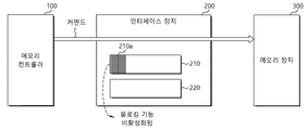
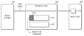
도 2는 본 발명의 실시 예에 따라, 인터페이스 장치가 인터페이싱 동작을 수행하는 방법을 도시하는 도면,
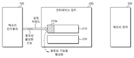
도 3은 본 발명의 실시 예에 따라, 메모리 컨트롤러가 인터페이스 장치의 블로킹 기능을 활성화시키는 방법을 도시하는 도면,
도 4는 본 발명의 실시 예에 따라, 메모리 컨트롤러가 인터페이스 장치의 인터페이스 설정 동작을 제어하는 방법을 도시하는 도면,
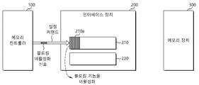
도 5는 본 발명의 실시 예에 따라, 메모리 컨트롤러가 인터페이스 장치의 블로킹 기능을 비활성화시키는 방법을 도시하는 도면,
도 6은 본 발명의 실시 예에 따라, 인터페이스 장치가 설정 커맨드에 대해 인터페이싱 동작을 수행하는 방법을 도시하는 도면,
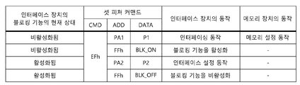
도 7은 본 발명의 실시 예에 따라 셋 피쳐(set feature) 커맨드의 사용 방법을 도시한 도면,
도 8은 본 발명의 다른 실시 예에 따른 메모리 시스템을 예시적으로 도시하는 도면,
도 9는 본 발명의 실시 예에 따른 메모리 시스템을 포함하는 데이터 처리 시스템을 예시적으로 도시하는 도면,
도 10은 본 발명의 실시 예에 따른 메모리 시스템을 포함하는 데이터 처리 시스템을 예시적으로 도시하는 도면,
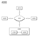
도 11은 본 발명의 실시 예에 따른 메모리 시스템을 포함하는 네트워크 시스템을 예시적으로 도시하는 도면,
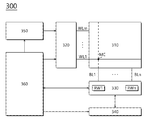
도 12는 본 발명의 실시 예에 따른 메모리 시스템에 포함된 비휘발성 메모리 장치를 예시적으로 도시하는 블럭도이다.
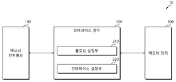
200: 인터페이스 장치 210: 블로킹 설정부
220: 인터페이스 설정부 300: 메모리 장치
Claims (21)
- 메모리 장치;
상기 메모리 장치를 제어하도록 구성된 메모리 컨트롤러; 및
상기 메모리 장치와 상기 메모리 컨트롤러 사이의 제어 신호 및 데이터 전송을 위한 인터페이싱 동작을 수행하도록 구성된 인터페이스 장치를 포함하되,
상기 인터페이스 장치는, 상기 메모리 컨트롤러의 블로킹 활성화 신호를 포함하는 설정 커맨드에 응답하여 상기 인터페이스 동작에 대한 블로킹 기능을 활성화시키고, 상기 블로킹 기능이 활성화된 동안에 상기 메모리 컨트롤러의 인터페이스 설정 커맨드에 응답하여 인터페이스 설정 동작을 수행하는 메모리 시스템. - 제1항에 있어서,
상기 인터페이스 장치는,
블로킹 설정부를 포함하고,
상기 설정 커맨드가 상기 블로킹 설정부의 어드레스를 포함할 때, 상기 블로킹 설정부에 상기 블로킹 활성화 신호를 저장함으로써 상기 블로킹 기능을 활성화시키는 메모리 시스템. - 제1항에 있어서,
상기 인터페이스 장치는 상기 블로킹 기능이 활성화된 동안에 블로킹 비활성화 신호를 포함하는 상기 설정 커맨드에 응답하여 상기 블로킹 기능을 비활성화시키는 메모리 시스템. - 제3항에 있어서,
상기 인터페이스 장치는,
블로킹 설정부를 포함하고,
상기 설정 커맨드가 상기 블로킹 설정부의 어드레스를 포함할 때, 상기 블로킹 설정부에 상기 블로킹 활성화 신호 또는 상기 블로킹 비활성화 신호를 저장함으로써 상기 블로킹 기능을 활성화시키거나 또는 비활성화시키는 메모리 시스템. - 제1항에 있어서,
상기 인터페이스 장치는,
상기 인터페이싱 동작을 수행하기 위해 참조하는 인터페이스 설정 값이 저장된 인터페이스 설정부를 포함하고,
상기 인터페이스 설정부의 어드레스를 포함하는 상기 인터페이스 설정 커맨드에 응답하여 상기 인터페이스 설정 동작을 수행함으로써 상기 인터페이스 설정 값을 조정하는 메모리 시스템. - 제1항에 있어서,
상기 인터페이스 장치는 상기 블로킹 기능이 비활성화된 동안에 커맨드를 수신할 경우, 상기 인터페이싱 동작을 수행함으로써 상기 메모리 장치로 상기 커맨드를 전송하는 메모리 시스템. - 제1항에 있어서,
상기 메모리 장치는 내부 동작을 수행하기 위해 참조하는 메모리 설정 값이 저장된 메모리 설정부를 포함하고,
상기 인터페이스 장치는 상기 블로킹 기능이 비활성화된 동안에 상기 메모리 설정부의 어드레스를 포함하는 상기 설정 커맨드에 응답하여, 상기 인터페이싱 동작을 수행함으로써 상기 메모리 장치로 상기 설정 커맨드를 전송하고,
상기 메모리 장치는 상기 설정 커맨드에 응답하여 상기 메모리 설정 값을 조정하는 메모리 시스템. - 메모리 장치;
상기 메모리 장치를 제어하기 위한 커맨드를 생성하도록 구성된 메모리 컨트롤러; 및
블로킹 기능이 비활성화된 동안에 상기 메모리 컨트롤러로부터 전송된 상기 커맨드에 응답하여, 인터페이싱 동작을 수행함으로써 상기 메모리 장치로 상기 커맨드를 전송하도록 구성된 인터페이스 장치를 포함하되,
상기 메모리 컨트롤러는 블로킹 활성화 신호를 포함하는 상기 커맨드를 상기 인터페이스 장치로 전송하고,
상기 인터페이스 장치는 상기 블로킹 활성화 신호를 포함하는 상기 커맨드에 응답하여 상기 블로킹 기능을 활성화시키고, 상기 블로킹 기능이 활성화된 동안에 상기 인터페이싱 동작을 수행하지 않는 메모리 시스템. - 제8항에 있어서,
상기 인터페이스 장치는 블로킹 설정부를 포함하고,
상기 메모리 컨트롤러는 상기 블로킹 설정부의 어드레스 및 상기 블로킹 활성화 신호를 포함하는 상기 커맨드를 상기 인터페이스 장치로 전송하고,
상기 인터페이스 장치는 상기 어드레스를 인식하고 상기 블로킹 설정부에 상기 블로킹 활성화 신호를 저장함으로써, 상기 블로킹 기능을 활성화시키는 메모리 시스템. - 제8항에 있어서,
상기 메모리 컨트롤러는 상기 블로킹 기능이 활성화된 동안에 블로킹 비활성화 신호를 포함하는 상기 커맨드를 상기 인터페이스로 전송하고,
상기 인터페이스는 상기 블로킹 비활성화 신호를 포함하는 상기 커맨드에 응답하여 상기 블로킹 기능을 비활성화시키는 메모리 시스템. - 제10항에 있어서,
상기 인터페이스 장치는 블로킹 설정부를 포함하고,
상기 메모리 컨트롤러는 상기 블로킹 설정부의 어드레스 및 상기 블로킹 비활성화 신호를 포함하는 상기 커맨드를 상기 인터페이스 장치로 전송하고,
상기 인터페이스 장치는 상기 어드레스를 인식하고 상기 블로킹 설정부에 상기 블로킹 비활성화 신호를 저장함으로써, 상기 블로킹 기능을 비활성화시키는 메모리 시스템. - 제8항에 있어서,
상기 메모리 컨트롤러는 상기 블로킹 기능이 활성화된 동안에 인터페이스 설정 커맨드를 상기 인터페이스 장치로 전송하고,
상기 인터페이스 장치는 상기 인터페이스 설정 커맨드에 응답하여 상기 인터페이싱 동작을 수행하기 위해 참조하는 인터페이스 설정 값을 조정하는 메모리 시스템. - 제12항에 있어서,
상기 인터페이스 장치는 상기 인터페이스 설정 값이 저장된 인터페이스 설정부를 포함하고,
상기 메모리 컨트롤러는 상기 인터페이스 설정부의 어드레스를 포함하는 상기 인터페이스 설정 커맨드를 상기 인터페이스 장치로 전송하고,
상기 인터페이스 장치는 상기 인터페이스 설정 커맨드에 응답하여 상기 어드레스를 인식하고 상기 인터페이스 설정 값을 조정하는 메모리 시스템. - 제8항에 있어서,
상기 메모리 장치는 내부 동작을 수행하기 위해 참조하는 메모리 설정 값이 저장된 메모리 설정부를 포함하고,
상기 메모리 컨트롤러는 상기 블로킹 기능이 비활성화된 동안에 상기 메모리 설정부의 어드레스를 포함하는 상기 커맨드를 상기 인터페이스 장치로 전송하고,
상기 인터페이스 장치는 상기 메모리 설정부의 어드레스를 포함하는 상기 커맨드에 응답하여, 상기 인터페이싱 동작을 수행함으로써 상기 메모리 장치로 상기 커맨드를 전송하고,
상기 메모리 장치는 상기 커맨드에 응답하여 상기 어드레스를 인식하고 상기 메모리 설정 값을 조정하는 메모리 시스템. - 메모리 장치;
메모리 컨트롤러; 및
상기 메모리 장치와 상기 메모리 컨트롤러 사이에서 인터페이싱 동작을 수행하고, 블로킹 설정부를 포함하도록 구성된 인터페이스 장치를 포함하되,
상기 메모리 컨트롤러는 상기 블로킹 설정부를 액세스함으로써 상기 인터페이스 장치의 블로킹 기능을 활성화시키고,
상기 인터페이스 장치는 상기 블로킹 기능이 활성화된 동안에, 상기 인터페이싱 동작을 수행하지 않는 메모리 시스템. - 제15항에 있어서,
상기 메모리 컨트롤러는 상기 블로킹 설정부의 어드레스 및 블로킹 활성화 신호를 포함하는 설정 커맨드를 상기 인터페이스로 전송하고,
상기 인터페이스는 상기 설정 커맨드에 응답하여 상기 어드레스를 인식하고 상기 블로킹 설정부에 상기 블로킹 활성화 신호를 저장함으로써 상기 블로킹 기능을 활성화시키는 메모리 시스템. - 제15항에 있어서,
상기 메모리 컨트롤러는 상기 블로킹 기능이 활성화된 동안에, 상기 블로킹 설정부의 어드레스 및 블로킹 비활성화 신호를 포함하는 설정 커맨드를 상기 인터페이스 장치로 전송하고,
상기 인터페이스 장치는 상기 설정 커맨드에 응답하여 상기 어드레스를 인식하고 상기 블로킹 설정부에 상기 블로킹 비활성화 신호를 저장함으로써 상기 블로킹 기능을 비활성화시키는 메모리 시스템. - 제15항에 있어서,
상기 메모리 컨트롤러는 상기 블로킹 기능이 활성화된 동안에 인터페이스 설정 커맨드를 상기 인터페이스 장치로 전송하고,
상기 인터페이스 장치는 상기 인터페이스 설정 커맨드에 응답하여 상기 인터페이싱 동작을 수행하기 위해 참조하는 인터페이스 설정 값을 조정하는 메모리 시스템. - 제15항에 있어서,
상기 인터페이스 장치는 상기 인터페이스 설정 값이 저장된 인터페이스 설정부를 포함하고,
상기 메모리 컨트롤러는 상기 인터페이스 설정부의 어드레스를 포함하는 상기 인터페이스 설정 커맨드를 상기 인터페이스 장치로 전송하고,
상기 인터페이스 장치는 상기 인터페이스 설정 커맨드에 응답하여 상기 어드레스를 인식하고 상기 인터페이스 설정 값을 조정하는 메모리 시스템. - 제15항에 있어서,
상기 인터페이스 장치는 상기 블로킹 기능이 비활성화된 동안에 상기 인터페이싱 동작을 수행하는 메모리 시스템. - 제15항에 있어서,
상기 메모리 장치는 내부 동작을 수행하기 위해 참조하는 메모리 설정 값이 저장된 메모리 설정부를 포함하고,
상기 메모리 컨트롤러는 상기 블로킹 기능이 비활성화된 동안에 상기 메모리 설정부의 어드레스를 포함하는 설정 커맨드를 상기 인터페이스 장치로 전송하고,
상기 인터페이스 장치는 상기 인터페이싱 동작을 수행함으로써 상기 메모리 장치로 상기 설정 커맨드를 전송하고,
상기 메모리 장치는 상기 설정 커맨드에 응답하여 상기 어드레스를 인식하고 상기 메모리 설정 값을 조정하는 메모리 시스템.
Priority Applications (4)
| Application Number | Priority Date | Filing Date | Title |
|---|---|---|---|
| KR1020190010756A KR102811682B1 (ko) | 2019-01-28 | 2019-01-28 | 메모리 시스템 |
| US16/570,315 US11042493B2 (en) | 2019-01-28 | 2019-09-13 | Memory system |
| CN201910972964.5A CN111488296B (zh) | 2019-01-28 | 2019-10-14 | 存储器系统 |
| US17/350,341 US11593285B2 (en) | 2019-01-28 | 2021-06-17 | Memory system |
Applications Claiming Priority (1)
| Application Number | Priority Date | Filing Date | Title |
|---|---|---|---|
| KR1020190010756A KR102811682B1 (ko) | 2019-01-28 | 2019-01-28 | 메모리 시스템 |
Publications (2)
| Publication Number | Publication Date |
|---|---|
| KR20200093363A true KR20200093363A (ko) | 2020-08-05 |
| KR102811682B1 KR102811682B1 (ko) | 2025-05-22 |
Family
ID=71732562
Family Applications (1)
| Application Number | Title | Priority Date | Filing Date |
|---|---|---|---|
| KR1020190010756A Active KR102811682B1 (ko) | 2019-01-28 | 2019-01-28 | 메모리 시스템 |
Country Status (3)
| Country | Link |
|---|---|
| US (2) | US11042493B2 (ko) |
| KR (1) | KR102811682B1 (ko) |
| CN (1) | CN111488296B (ko) |
Families Citing this family (1)
| Publication number | Priority date | Publication date | Assignee | Title |
|---|---|---|---|---|
| KR102811682B1 (ko) * | 2019-01-28 | 2025-05-22 | 에스케이하이닉스 주식회사 | 메모리 시스템 |
Citations (5)
| Publication number | Priority date | Publication date | Assignee | Title |
|---|---|---|---|---|
| US20080126749A1 (en) * | 2006-11-07 | 2008-05-29 | Spansion Llc | Using shared memory with an execute-in-place processor and a co-processor |
| US20080256374A1 (en) * | 2007-04-10 | 2008-10-16 | Harris Ian F | Sharing Non-Sharable Devices Between an Embedded Controller and A Processor in a Computer System |
| US20120221769A1 (en) * | 2008-07-23 | 2012-08-30 | Rambus Inc. | Reconfigurable memory controller |
| KR20130114354A (ko) * | 2012-04-09 | 2013-10-18 | 삼성전자주식회사 | 메모리 시스템 및 컨트롤러의 동작 방법 |
| KR20150051673A (ko) * | 2013-11-05 | 2015-05-13 | 에스케이하이닉스 주식회사 | 메모리 장치 및 이를 포함하는 시스템 |
Family Cites Families (13)
| Publication number | Priority date | Publication date | Assignee | Title |
|---|---|---|---|---|
| JP2003297080A (ja) * | 2002-03-29 | 2003-10-17 | Mitsubishi Electric Corp | 半導体記憶装置 |
| KR100816053B1 (ko) * | 2006-11-21 | 2008-03-21 | 엠텍비젼 주식회사 | 셀프 카피 기능을 가지는 메모리 장치, 메모리 시스템 및듀얼 포트 메모리 장치 |
| TWI413898B (zh) * | 2009-09-15 | 2013-11-01 | Phison Electronics Corp | 資料保護方法與系統、儲存裝置及儲存裝置控制器 |
| US8527825B2 (en) * | 2010-09-21 | 2013-09-03 | Qualcomm Incorporated | Debugger based memory dump using built in self test |
| KR101522293B1 (ko) | 2013-08-29 | 2015-05-21 | 주식회사 유니테스트 | 복수개의 스토리지를 개별 제어 가능한 테스트 장치 |
| US9729320B2 (en) * | 2014-02-25 | 2017-08-08 | Cavium, Inc. | Apparatus and method for software enabled access to protected hardware resources |
| KR102251809B1 (ko) | 2014-05-28 | 2021-05-13 | 삼성전자주식회사 | 메모리 시스템, 메모리 인터페이스 장치 및 메모리 시스템에서의 인터페이싱 방법 |
| KR102389232B1 (ko) * | 2015-10-16 | 2022-04-22 | 에스케이하이닉스 주식회사 | 메모리 장치 및 이를 포함하는 시스템 |
| US10430361B1 (en) * | 2015-12-17 | 2019-10-01 | Cru Acquisition Group, Llc | Combination write blocker |
| CN108345808B (zh) * | 2017-01-25 | 2021-12-31 | 三星电子株式会社 | 非易失性存储器件和包括非易失性存储器件的固态驱动器 |
| KR102519572B1 (ko) * | 2018-05-11 | 2023-04-07 | 에스케이하이닉스 주식회사 | 메모리 시스템 및 메모리 시스템의 동작 방법 |
| US11086803B2 (en) * | 2018-10-05 | 2021-08-10 | Micron Technology, Inc. | Dynamically configuring transmission lines of a bus |
| KR102811682B1 (ko) * | 2019-01-28 | 2025-05-22 | 에스케이하이닉스 주식회사 | 메모리 시스템 |
-
2019
- 2019-01-28 KR KR1020190010756A patent/KR102811682B1/ko active Active
- 2019-09-13 US US16/570,315 patent/US11042493B2/en active Active
- 2019-10-14 CN CN201910972964.5A patent/CN111488296B/zh active Active
-
2021
- 2021-06-17 US US17/350,341 patent/US11593285B2/en active Active
Patent Citations (5)
| Publication number | Priority date | Publication date | Assignee | Title |
|---|---|---|---|---|
| US20080126749A1 (en) * | 2006-11-07 | 2008-05-29 | Spansion Llc | Using shared memory with an execute-in-place processor and a co-processor |
| US20080256374A1 (en) * | 2007-04-10 | 2008-10-16 | Harris Ian F | Sharing Non-Sharable Devices Between an Embedded Controller and A Processor in a Computer System |
| US20120221769A1 (en) * | 2008-07-23 | 2012-08-30 | Rambus Inc. | Reconfigurable memory controller |
| KR20130114354A (ko) * | 2012-04-09 | 2013-10-18 | 삼성전자주식회사 | 메모리 시스템 및 컨트롤러의 동작 방법 |
| KR20150051673A (ko) * | 2013-11-05 | 2015-05-13 | 에스케이하이닉스 주식회사 | 메모리 장치 및 이를 포함하는 시스템 |
Also Published As
| Publication number | Publication date |
|---|---|
| US20200242056A1 (en) | 2020-07-30 |
| CN111488296B (zh) | 2023-08-01 |
| US20210311890A1 (en) | 2021-10-07 |
| CN111488296A (zh) | 2020-08-04 |
| US11593285B2 (en) | 2023-02-28 |
| US11042493B2 (en) | 2021-06-22 |
| KR102811682B1 (ko) | 2025-05-22 |
Similar Documents
| Publication | Publication Date | Title |
|---|---|---|
| US11101017B2 (en) | Memory system and test system | |
| US20180130537A1 (en) | Data storage device and operating method thereof | |
| US11704048B2 (en) | Electronic device | |
| US20190220228A1 (en) | Memory system and operating method thereof | |
| US20200150898A1 (en) | Memory system and operating method thereof | |
| US12026398B2 (en) | Memory system performing flush operation for buffer region | |
| KR20190076296A (ko) | 메모리 시스템 및 그것의 동작 방법 | |
| US20190088293A1 (en) | Nonvolatile memory device, data storage device including the same and operating method thereof | |
| KR102782782B1 (ko) | 불휘발성 메모리 장치의 동작 방법 및 그것을 포함하는 데이터 저장 장치의 동작 방법 | |
| US10629275B2 (en) | Data storage device and operating method thereof | |
| KR20200072620A (ko) | 전자 장치 | |
| US10776008B2 (en) | Memory system and operating method thereof | |
| US11593285B2 (en) | Memory system | |
| KR102475688B1 (ko) | 불휘발성 메모리 장치, 이를 포함하는 데이터 저장 장치 및 그것의 동작 방법 | |
| US11544004B2 (en) | Nonvolatile memory device and memory system including the same | |
| US10553292B1 (en) | Memory system with memory region read counts and a memory group read count and operating method thereof | |
| KR20210094773A (ko) | 메모리 시스템 및 그것을 포함하는 데이터 처리 시스템 |
Legal Events
| Date | Code | Title | Description |
|---|---|---|---|
| PA0109 | Patent application |
Patent event code: PA01091R01D Comment text: Patent Application Patent event date: 20190128 |
|
| PG1501 | Laying open of application | ||
| A201 | Request for examination | ||
| PA0201 | Request for examination |
Patent event code: PA02012R01D Patent event date: 20220128 Comment text: Request for Examination of Application Patent event code: PA02011R01I Patent event date: 20190128 Comment text: Patent Application |
|
| E902 | Notification of reason for refusal | ||
| PE0902 | Notice of grounds for rejection |
Comment text: Notification of reason for refusal Patent event date: 20240822 Patent event code: PE09021S01D |
|
| E701 | Decision to grant or registration of patent right | ||
| PE0701 | Decision of registration |
Patent event code: PE07011S01D Comment text: Decision to Grant Registration Patent event date: 20250401 |
|
| GRNT | Written decision to grant | ||
| PR0701 | Registration of establishment |
Comment text: Registration of Establishment Patent event date: 20250519 Patent event code: PR07011E01D |
|
| PR1002 | Payment of registration fee |
Payment date: 20250520 End annual number: 3 Start annual number: 1 |
|
| PG1601 | Publication of registration |