KR20200093726A - 디지털 제어형 벡터 신호 변조기 - Google Patents
디지털 제어형 벡터 신호 변조기 Download PDFInfo
- Publication number
- KR20200093726A KR20200093726A KR1020190010480A KR20190010480A KR20200093726A KR 20200093726 A KR20200093726 A KR 20200093726A KR 1020190010480 A KR1020190010480 A KR 1020190010480A KR 20190010480 A KR20190010480 A KR 20190010480A KR 20200093726 A KR20200093726 A KR 20200093726A
- Authority
- KR
- South Korea
- Prior art keywords
- phase
- switching
- orthogonal
- bits
- signal
- Prior art date
- Legal status (The legal status is an assumption and is not a legal conclusion. Google has not performed a legal analysis and makes no representation as to the accuracy of the status listed.)
- Ceased
Links
Images


Classifications
-
- H—ELECTRICITY
- H04—ELECTRIC COMMUNICATION TECHNIQUE
- H04L—TRANSMISSION OF DIGITAL INFORMATION, e.g. TELEGRAPHIC COMMUNICATION
- H04L27/00—Modulated-carrier systems
- H04L27/32—Carrier systems characterised by combinations of two or more of the types covered by groups H04L27/02, H04L27/10, H04L27/18 or H04L27/26
- H04L27/34—Amplitude- and phase-modulated carrier systems, e.g. quadrature-amplitude modulated carrier systems
- H04L27/36—Modulator circuits; Transmitter circuits
- H04L27/362—Modulation using more than one carrier, e.g. with quadrature carriers, separately amplitude modulated
-
- H—ELECTRICITY
- H03—ELECTRONIC CIRCUITRY
- H03F—AMPLIFIERS
- H03F3/00—Amplifiers with only discharge tubes or only semiconductor devices as amplifying elements
- H03F3/45—Differential amplifiers
- H03F3/45071—Differential amplifiers with semiconductor devices only
- H03F3/45076—Differential amplifiers with semiconductor devices only characterised by the way of implementation of the active amplifying circuit in the differential amplifier
- H03F3/45475—Differential amplifiers with semiconductor devices only characterised by the way of implementation of the active amplifying circuit in the differential amplifier using IC blocks as the active amplifying circuit
-
- H—ELECTRICITY
- H04—ELECTRIC COMMUNICATION TECHNIQUE
- H04L—TRANSMISSION OF DIGITAL INFORMATION, e.g. TELEGRAPHIC COMMUNICATION
- H04L27/00—Modulated-carrier systems
- H04L27/18—Phase-modulated carrier systems, i.e. using phase-shift keying
-
- H—ELECTRICITY
- H03—ELECTRONIC CIRCUITRY
- H03C—MODULATION
- H03C3/00—Angle modulation
- H03C3/38—Angle modulation by converting amplitude modulation to angle modulation
- H03C3/40—Angle modulation by converting amplitude modulation to angle modulation using two signal paths the outputs of which have a predetermined phase difference and at least one output being amplitude-modulated
-
- H—ELECTRICITY
- H03—ELECTRONIC CIRCUITRY
- H03C—MODULATION
- H03C5/00—Amplitude modulation and angle modulation produced simultaneously or at will by the same modulating signal
-
- H—ELECTRICITY
- H03—ELECTRONIC CIRCUITRY
- H03D—DEMODULATION OR TRANSFERENCE OF MODULATION FROM ONE CARRIER TO ANOTHER
- H03D7/00—Transference of modulation from one carrier to another, e.g. frequency-changing
- H03D7/16—Multiple-frequency-changing
- H03D7/165—Multiple-frequency-changing at least two frequency changers being located in different paths, e.g. in two paths with carriers in quadrature
- H03D7/166—Multiple-frequency-changing at least two frequency changers being located in different paths, e.g. in two paths with carriers in quadrature using two or more quadrature frequency translation stages
-
- H—ELECTRICITY
- H03—ELECTRONIC CIRCUITRY
- H03F—AMPLIFIERS
- H03F3/00—Amplifiers with only discharge tubes or only semiconductor devices as amplifying elements
- H03F3/189—High-frequency amplifiers, e.g. radio frequency amplifiers
- H03F3/19—High-frequency amplifiers, e.g. radio frequency amplifiers with semiconductor devices only
-
- H—ELECTRICITY
- H03—ELECTRONIC CIRCUITRY
- H03F—AMPLIFIERS
- H03F3/00—Amplifiers with only discharge tubes or only semiconductor devices as amplifying elements
- H03F3/189—High-frequency amplifiers, e.g. radio frequency amplifiers
- H03F3/19—High-frequency amplifiers, e.g. radio frequency amplifiers with semiconductor devices only
- H03F3/195—High-frequency amplifiers, e.g. radio frequency amplifiers with semiconductor devices only in integrated circuits
-
- H—ELECTRICITY
- H03—ELECTRONIC CIRCUITRY
- H03F—AMPLIFIERS
- H03F3/00—Amplifiers with only discharge tubes or only semiconductor devices as amplifying elements
- H03F3/45—Differential amplifiers
- H03F3/45071—Differential amplifiers with semiconductor devices only
-
- H—ELECTRICITY
- H03—ELECTRONIC CIRCUITRY
- H03F—AMPLIFIERS
- H03F3/00—Amplifiers with only discharge tubes or only semiconductor devices as amplifying elements
- H03F3/68—Combinations of amplifiers, e.g. multi-channel amplifiers for stereophonics
-
- H—ELECTRICITY
- H03—ELECTRONIC CIRCUITRY
- H03G—CONTROL OF AMPLIFICATION
- H03G3/00—Gain control in amplifiers or frequency changers
- H03G3/001—Digital control of analog signals
-
- H—ELECTRICITY
- H03—ELECTRONIC CIRCUITRY
- H03G—CONTROL OF AMPLIFICATION
- H03G3/00—Gain control in amplifiers or frequency changers
- H03G3/20—Automatic control
- H03G3/30—Automatic control in amplifiers having semiconductor devices
- H03G3/3052—Automatic control in amplifiers having semiconductor devices in bandpass amplifiers (H.F. or I.F.) or in frequency-changers used in a (super)heterodyne receiver
-
- H—ELECTRICITY
- H04—ELECTRIC COMMUNICATION TECHNIQUE
- H04L—TRANSMISSION OF DIGITAL INFORMATION, e.g. TELEGRAPHIC COMMUNICATION
- H04L27/00—Modulated-carrier systems
- H04L27/18—Phase-modulated carrier systems, i.e. using phase-shift keying
- H04L27/20—Modulator circuits; Transmitter circuits
- H04L27/2032—Modulator circuits; Transmitter circuits for discrete phase modulation, e.g. in which the phase of the carrier is modulated in a nominally instantaneous manner
- H04L27/2053—Modulator circuits; Transmitter circuits for discrete phase modulation, e.g. in which the phase of the carrier is modulated in a nominally instantaneous manner using more than one carrier, e.g. carriers with different phases
- H04L27/206—Modulator circuits; Transmitter circuits for discrete phase modulation, e.g. in which the phase of the carrier is modulated in a nominally instantaneous manner using more than one carrier, e.g. carriers with different phases using a pair of orthogonal carriers, e.g. quadrature carriers
-
- H—ELECTRICITY
- H04—ELECTRIC COMMUNICATION TECHNIQUE
- H04L—TRANSMISSION OF DIGITAL INFORMATION, e.g. TELEGRAPHIC COMMUNICATION
- H04L27/00—Modulated-carrier systems
- H04L27/32—Carrier systems characterised by combinations of two or more of the types covered by groups H04L27/02, H04L27/10, H04L27/18 or H04L27/26
- H04L27/34—Amplitude- and phase-modulated carrier systems, e.g. quadrature-amplitude modulated carrier systems
- H04L27/36—Modulator circuits; Transmitter circuits
- H04L27/365—Modulation using digital generation of the modulated carrier (not including modulation of a digitally generated carrier)
-
- H—ELECTRICITY
- H03—ELECTRONIC CIRCUITRY
- H03F—AMPLIFIERS
- H03F2200/00—Indexing scheme relating to amplifiers
- H03F2200/336—A I/Q, i.e. phase quadrature, modulator or demodulator being used in an amplifying circuit
-
- H—ELECTRICITY
- H03—ELECTRONIC CIRCUITRY
- H03F—AMPLIFIERS
- H03F2200/00—Indexing scheme relating to amplifiers
- H03F2200/421—Multiple switches coupled in the output circuit of an amplifier are controlled by a circuit
-
- H—ELECTRICITY
- H03—ELECTRONIC CIRCUITRY
- H03F—AMPLIFIERS
- H03F2200/00—Indexing scheme relating to amplifiers
- H03F2200/451—Indexing scheme relating to amplifiers the amplifier being a radio frequency amplifier
Landscapes
- Engineering & Computer Science (AREA)
- Power Engineering (AREA)
- Computer Networks & Wireless Communication (AREA)
- Signal Processing (AREA)
- Microelectronics & Electronic Packaging (AREA)
- Digital Transmission Methods That Use Modulated Carrier Waves (AREA)
- Transmitters (AREA)
Abstract
Description
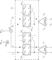
도 2는 본 발명의 일 실시예에 따른 스위칭 회로의 개략도이다.
도 3은 도 2의 스위칭 회로의 도통 상태(conduction status)의 개략도이다.
도 4는 본 발명의 일 실시예에 따른 스위칭 회로의 개략도이다.
Claims (6)
- 입력 무선 주파수(radio frequency, RF) 신호에 따라 입력 동위상 신호 및 입력 직교 신호를 생성하도록 구성된 직교 성분 생성기;
복수의 비트를 수신하고, 상기 복수의 비트에 의해 제어되는 복수의 스위치를 포함하며, 상기 복수의 비트에 따라 출력 동위상 신호 및 출력 직교 신호를 생성하도록 구성된 스위칭 회로 - 상기 출력 동위상 신호 및 상기 출력 직교 신호는 상기 입력 동위상 신호 및 상기 입력 직교 신호와 관련됨 -; 및
상기 출력 동영상 신호 및 상기 출력 직교 신호에 따라 출력 RF 신호를 생성하도록 구성된 결합 모듈
을 포함하는 벡터 변조기. - 제1항에있어서,
상기 스위칭 회로는,
상기 직교 성분 생생기에 연결된 스위칭 입력 단자;
상기 결합 모듈에 연결된 스위칭 출력 단자;
상기 스위칭 입력 단자와 상기 스위칭 출력 단자 사이에 연결되고, 상기 복수의 비트 내의 복수의 도통 비트(conducting bit)에 의해 제어되는 복수의 도통 스위치; 및
상기 스위칭 입력 단자에 연결되고 전압을 수신하며, 상기 복수의 비트 내의 복수의 전환 비트(diverting bit)에 의해 제어되는 복수의 전환 스위치 - 상기 복수의 전환 비트는 상기 복수의 도통 비트의 보수임 -를 포함하는, 벡터 변조기. - 제1항에 있어서,
상기 직교 성분 생성기와 상기 스위칭 회로 사이에 연결되고, 상기 입력 동위상 신호를 수신하여 중간 동위상 신호를 출력하도록 구성된 동위상 증폭기; 및
상기 직교 성분 생성기와 상기 스위칭 회로 사이에 연결되고, 상기 입력 직교 신호를 수신하여 중간 직교 신호를 출력하도록 구성된 직교 증폭기를 더 포함하는 벡터 변조기. - 제3항에 있어서,
상기 입력 동위상 신호는 제1 입력 동위상 신호 및 제2 입력 동위상 신호를 포함하고;
상기 입력 직교 신호는 제1 입력 직교 신호 및 제2 입력 직교 신호를 포함하고;
상기 동위상 증폭기는 제1 동위상 출력 단자 및 제2 동위상 출력 단자를 포함하고;
상기 직교 증폭기는 제1 직교 출력 단자 및 제2 직교 출력 단자를 포함하고;
상기 중간 동위상 신호는 제1 중간 동위상 신호 및 음의 중간 동위상 신호를 포함하고;
상기 중간 직교 신호는 제1 중간 직교 신호 및 음의 중간 직교 신호를 포함하고;
상기 출력 동위상 신호는 제1 출력 동위상 신호 및 제2 출력 동위상 신호를 포함하고;
상기 출력 직교 신호는 제1 출력 직교 신호 및 제2 출력 직교 신호를 포함하고;
상기 출력 RF 신호는 제1 출력 RF 신호 및 제2 출력 RF 신호를 포함하며;
상기 결합 모듈은,
상기 제1 출력 동위상 신호 및 상기 제1 출력 직교 신호에 따라 상기 제1 출력 RF 신호를 생성하도록 구성된 제1 결합 요소; 및
상기 제2 출력 동위상 신호 및 상기 제2 출력 직교 신호에 따라 상기 제2 출력 RF 신호를 생성하도록 구성된 제2 결합 요소를 포함하는, 벡터 변조기. - 제4항에 있어서,
상기 스위칭 회로는,
제1 동위상 스위칭 서브회로; 및
제1 직교 스위칭 서브회로를 포함하고,
상기 제1 동위상 스위칭 서브회로는,
상기 동위상 증폭기의 제1 동위상 출력 단자에 연결된 제1 동위상 스위칭 입력 단자;
상기 동위상 증폭기의 제2 동위상 출력 단자에 연결된 제2 동위상 스위칭 입력 단자;
제1 동위상 스위칭 출력 단자;
제2 동위상 스위칭 출력 단자;
상기 제1 동위상 스위칭 입력 단자와 상기 제1 동위상 스위칭 출력 단자 사이에 연결되고, 상기 복수의 비트 내의 복수의 동위상 도통 비트에 의해 제어되는 복수의 제1 동위상 도통 스위치;
상기 제2 동위상 스위칭 입력 단자와 상기 제2 동위상 스위칭 출력 단자 사이에 연결되고, 상기 복수의 비트 내의 복수의 동위상 도통 비트에 의해 제어되는 복수의 제2 동위상 도통 스위치;
상기 제1 동위상 스위칭 입력 단자에 결합되어 전압을 수신하고, 상기 복수의 비트 내의 복수의 동위상 전환 비트에 의해 제어되는 복수의 제1 동위상 전환 스위치 - 상기 복수의 동위상 전환 비트는 상기 복수의 동위상 도통 비트의 보수임 -; 및
상기 제2 동위상 스위칭 입력 단자에 연결되어 상기 전압을 수신하고, 상기 복수의 동위상 전환 비트에 의해 제어되는 복수의 제2 동위상 전환 스위치를 포함하고,
상기 제1 직교 스위칭 서브회로는,
상기 직교 증폭기의 제1 직교 출력 단자에 연결된 제1 직교 스위칭 입력 단자;
상기 직교 증폭기의 제2 직교 출력 단자에 연결된 제2 직교 스위칭 입력 단자;
제1 직교 스위칭 출력 단자;
제2 직교 스위칭 출력 단자;
상기 제1 직교 스위칭 입력 단자와 상기 제1 직교 스위칭 출력 단자 사이에 연결되고, 상기 복수의 비트 내의 복수의 직교 도통 비트에 의해 제어되는 복수의 제1 직교 도통 스위치;
상기 제2 직교 스위칭 입력 단자와 상기 제2 직교 스위칭 출력 단자 사이에 연결되고, 상기 복수의 비트 내의 복수의 직교 도통 비트에 의해 제어되는 복수의 제2 직교 도통 스위치;
상기 제1 직교 스위칭 입력 단자에 연결되어 상기 전압을 수신하고, 상기 복수의 비트 내의 복수의 직교 전환 비트에 의해 제어되는 복수의 제1 직교 전환 스위치 - 상기 복수의 직교 전환 비트는 상기 복수의 제1 직교 도통 비트의 보수임 -; 및
상기 제2 직교 스위칭 입력 단자에 연결되어 상기 전압을 수신하고, 상기 복수의 직교 전환 비트에 의해 제어되는 복수의 제2 직교 전환 스위치를 포함하는, 벡터 변조기. - 제5항에 있어서,
상기 스위칭 회로는,
제2 동위상 스위칭 서브회로; 및
제2 직교 스위칭 서브회로를 포함하고,
상기 제2 동위상 스위칭 서브회로는,
상기 동위상 증폭기의 제2 동위상 출력 단자에 연결된 제1 동위상 스위칭 입력 단자;
상기 동위상 증폭기의 제1 동위상 출력 단자에 연결된 제2 동위상 스위칭 입력 단자;
제1 동위상 스위칭 출력 단자;
제2 동위상 스위칭 출력 단자;
상기 제1 동위상 스위칭 입력 단자와 상기 제1 동위상 스위칭 출력 단자 사이에 연결되고, 상기 복수의 비트 내의 복수의 동위상 도통 비트에 의해 제어되는 복수의 제1 동위상 도통 스위치;
상기 제2 동위상 스위칭 입력 단자와 상기 제2 동위상 스위칭 출력 단자 사이에 연결되고, 상기 복수의 비트 내의 복수의 동위상 도통 비트에 의해 제어되는 복수의 제2 동위상 도통 스위치;
상기 제1 동위상 스위칭 입력 단자에 연결되어 상기 전압을 수신하고, 상기 복수의 비트 내의 복수의 동위상 전환 비트에 의해 제어되는 복수의 제1 동위상 전환 스위치 - 상기 복수의 제1 동위상 전환 비트는 상기 복수의 동위상 도통 비트의 보수임 -; 및
상기 제2 동위상 스위칭 입력 단자에 연결되어 상기 전압을 수신하고, 상기 복수의 동위상 전환 비트에 의해 제어되는 복수의 제2 동위상 전환 스위치를 포함하고,
상기 제2 직교 스위칭 서브회로는,
상기 직교 증폭기의 제2 직교 출력 단자에 연결된 제1 직교 스위칭 입력 단자;
상기 직교 증폭기의 제1 직교 출력 단자에 연결된 제2 직교 스위칭 입력 단자;
제1 직교 스위칭 출력 단자;
제2 직교 스위칭 출력 단자;
상기 제1 직교 스위칭 입력 단자와 상기 제1 직교 스위칭 출력 단자 사이에 연결되고, 상기 복수의 비트 내의 복수의 직교 도통 비트에 의해 제어되는 복수의 제1 직교 도통 스위치;
상기 제2 직교 스위칭 입력 단자와 상기 제2 직교 스위칭 출력 단자 사이에 연결되고, 상기 복수의 비트 내의 복수의 직교 도통 비트에 의해 제어되는 복수의 제2 직교 도통 스위치;
상기 제1 직교 스위칭 입력 단자에 연결되어 상기 전압을 수신하고, 상기 복수의 비트 내의 복수의 직교 전환 비트에 의해 제어되는 복수의 제1 직교 전환 스위치 - 상기 복수의 제1 직교 전환 비트는 상기 복수의 제1 직교 도통 비트의 보수임 -; 및
상기 제2 직교 스위칭 입력 단자에 연결되어 상기 전압을 수신하고, 상기 복수의 직교 전환 비트에 의해 제어되는 복수의 제2 직교 전환 스위치를 포함하는, 벡터 변조기.
Priority Applications (5)
| Application Number | Priority Date | Filing Date | Title |
|---|---|---|---|
| TW107144059A TWI675554B (zh) | 2018-12-07 | 2018-12-07 | 數位控制向量訊號調變器 |
| US16/234,484 US10476717B1 (en) | 2018-12-07 | 2018-12-27 | Digital-controlled vector signal modulator |
| EP19153196.1A EP3687064B1 (en) | 2018-12-07 | 2019-01-23 | Digital-controlled vector signal modulator |
| JP2019010748A JP6856677B2 (ja) | 2018-12-07 | 2019-01-25 | デジタル制御されるベクトル信号変調器 |
| KR1020190010480A KR20200093726A (ko) | 2018-12-07 | 2019-01-28 | 디지털 제어형 벡터 신호 변조기 |
Applications Claiming Priority (5)
| Application Number | Priority Date | Filing Date | Title |
|---|---|---|---|
| TW107144059A TWI675554B (zh) | 2018-12-07 | 2018-12-07 | 數位控制向量訊號調變器 |
| US16/234,484 US10476717B1 (en) | 2018-12-07 | 2018-12-27 | Digital-controlled vector signal modulator |
| EP19153196.1A EP3687064B1 (en) | 2018-12-07 | 2019-01-23 | Digital-controlled vector signal modulator |
| JP2019010748A JP6856677B2 (ja) | 2018-12-07 | 2019-01-25 | デジタル制御されるベクトル信号変調器 |
| KR1020190010480A KR20200093726A (ko) | 2018-12-07 | 2019-01-28 | 디지털 제어형 벡터 신호 변조기 |
Publications (1)
| Publication Number | Publication Date |
|---|---|
| KR20200093726A true KR20200093726A (ko) | 2020-08-06 |
Family
ID=92264564
Family Applications (1)
| Application Number | Title | Priority Date | Filing Date |
|---|---|---|---|
| KR1020190010480A Ceased KR20200093726A (ko) | 2018-12-07 | 2019-01-28 | 디지털 제어형 벡터 신호 변조기 |
Country Status (5)
| Country | Link |
|---|---|
| US (1) | US10476717B1 (ko) |
| EP (1) | EP3687064B1 (ko) |
| JP (1) | JP6856677B2 (ko) |
| KR (1) | KR20200093726A (ko) |
| TW (1) | TWI675554B (ko) |
Family Cites Families (16)
| Publication number | Priority date | Publication date | Assignee | Title |
|---|---|---|---|---|
| US4794621A (en) * | 1987-08-26 | 1988-12-27 | Josef Dirr | Apparatus for transmitting information by angle modulation |
| US4843351A (en) * | 1987-08-28 | 1989-06-27 | Hewlett-Packard Company | Vector modulation signal generator |
| US5317290A (en) * | 1987-10-19 | 1994-05-31 | General Electric Company | MMIC (monolithic microwave integrated circuit) switchable bidirectional phase shift network |
| US5355103A (en) * | 1990-06-29 | 1994-10-11 | American Nucleonics Corporation | Fast settling, wide dynamic range vector modulator |
| US7295819B2 (en) * | 2003-03-11 | 2007-11-13 | Andrew Corporation | Signal sample acquisition techniques |
| US6980779B2 (en) * | 2003-11-20 | 2005-12-27 | Nokia Corporation | RF transmitter using digital-to-RF conversion |
| US7355470B2 (en) * | 2006-04-24 | 2008-04-08 | Parkervision, Inc. | Systems and methods of RF power transmission, modulation, and amplification, including embodiments for amplifier class transitioning |
| US7609779B2 (en) * | 2006-02-27 | 2009-10-27 | Freescale Semiconductor, Inc. | RF transmitter with interleaved IQ modulation |
| TWI520439B (zh) * | 2009-04-13 | 2016-02-01 | 凡爾賽特公司 | 半雙工相位陣列天線系統 |
| KR101067470B1 (ko) | 2009-12-09 | 2011-09-27 | 한국과학기술원 | Iq 디지털 벡터 변조기 |
| US8699626B2 (en) | 2011-11-29 | 2014-04-15 | Viasat, Inc. | General purpose hybrid |
| US9246722B2 (en) * | 2012-03-20 | 2016-01-26 | Intel Deutschland Gmbh | Device for providing a differential output signal and method for providing a differential output signal |
| JP6163874B2 (ja) * | 2013-05-23 | 2017-07-19 | 株式会社リコー | 回転角度検出装置、画像処理装置及び回転角度検出方法 |
| US10700766B2 (en) * | 2017-04-19 | 2020-06-30 | Amir Keyvan Khandani | Noise cancelling amplify-and-forward (in-band) relay with self-interference cancellation |
| WO2018215647A1 (en) * | 2017-05-25 | 2018-11-29 | Technische Universiteit Eindhoven | Efficient wideband phased antenna array using true time delays and interpolation |
| CN108923797B (zh) * | 2018-06-25 | 2019-10-15 | 东南大学 | 一种应用于lte mtc电力物联网的新型发射机 |
-
2018
- 2018-12-07 TW TW107144059A patent/TWI675554B/zh active
- 2018-12-27 US US16/234,484 patent/US10476717B1/en active Active
-
2019
- 2019-01-23 EP EP19153196.1A patent/EP3687064B1/en active Active
- 2019-01-25 JP JP2019010748A patent/JP6856677B2/ja active Active
- 2019-01-28 KR KR1020190010480A patent/KR20200093726A/ko not_active Ceased
Also Published As
| Publication number | Publication date |
|---|---|
| EP3687064A1 (en) | 2020-07-29 |
| US10476717B1 (en) | 2019-11-12 |
| JP6856677B2 (ja) | 2021-04-07 |
| TW202023205A (zh) | 2020-06-16 |
| JP2020120302A (ja) | 2020-08-06 |
| EP3687064B1 (en) | 2022-02-16 |
| TWI675554B (zh) | 2019-10-21 |
Similar Documents
| Publication | Publication Date | Title |
|---|---|---|
| US9246722B2 (en) | Device for providing a differential output signal and method for providing a differential output signal | |
| US9800452B2 (en) | Digital quadrature modulator and switched-capacitor array circuit | |
| US11424725B2 (en) | Digital power amplifier with filtered output | |
| US8704606B2 (en) | Mixer cell, modulator and method | |
| KR100599148B1 (ko) | D급 증폭기를 제어하는 시스템 | |
| WO2018188501A1 (zh) | 一种数模转换器 | |
| EP2852051B1 (en) | Switch-mode amplifier | |
| US8867665B2 (en) | Communication systems and methods supporting multiple modulation techniques | |
| ES2744127T3 (es) | Estructura de amplificador de señal para radiotransmisor | |
| US10411348B2 (en) | Phase shifting device | |
| JP4881596B2 (ja) | 双方向周波数変換器およびこれを用いた無線機 | |
| EP2999116A1 (en) | Direct digital radio frequency modulator | |
| KR20200093726A (ko) | 디지털 제어형 벡터 신호 변조기 | |
| US10581395B2 (en) | Variable gain amplifier | |
| EP3843098B1 (en) | Sign switching circuitry | |
| US7852135B2 (en) | Circuit arrangement for signal mixing | |
| US7801498B2 (en) | Transmission of analog signals in a system-on-chip | |
| KR100770432B1 (ko) | 전류 미러링을 이용한 주파수 변환회로 | |
| EP4560918A1 (en) | Signal generation circuit | |
| KR20170077001A (ko) | 이진 가중치 가변 부하 | |
| EP4572140A1 (en) | Apparatuses, systems and methods for facilitating a phase shifter | |
| US20130082756A1 (en) | Signal input device of digital-rf converter | |
| EP4657754A1 (en) | Signal generation circuit | |
| KR20240049084A (ko) | 위상 천이기 | |
| WO2007125469A1 (en) | Power amplifier. |
Legal Events
| Date | Code | Title | Description |
|---|---|---|---|
| PA0109 | Patent application |
Patent event code: PA01091R01D Comment text: Patent Application Patent event date: 20190128 |
|
| PA0201 | Request for examination | ||
| PE0902 | Notice of grounds for rejection |
Comment text: Notification of reason for refusal Patent event date: 20200414 Patent event code: PE09021S01D |
|
| AMND | Amendment | ||
| PG1501 | Laying open of application | ||
| E601 | Decision to refuse application | ||
| PE0601 | Decision on rejection of patent |
Patent event date: 20201007 Comment text: Decision to Refuse Application Patent event code: PE06012S01D Patent event date: 20200414 Comment text: Notification of reason for refusal Patent event code: PE06011S01I |
|
| X091 | Application refused [patent] | ||
| PX0901 | Re-examination |
Patent event code: PX09011S01I Patent event date: 20201007 Comment text: Decision to Refuse Application Patent event code: PX09012R01I Patent event date: 20200603 Comment text: Amendment to Specification, etc. |
|
| E601 | Decision to refuse application | ||
| E801 | Decision on dismissal of amendment | ||
| PE0601 | Decision on rejection of patent |
Patent event date: 20201119 Comment text: Decision to Refuse Application Patent event code: PE06012S01D Patent event date: 20200414 Comment text: Notification of reason for refusal Patent event code: PE06011S01I |
|
| PE0801 | Dismissal of amendment |
Patent event code: PE08012E01D Comment text: Decision on Dismissal of Amendment Patent event date: 20201119 Patent event code: PE08011R01I Comment text: Amendment to Specification, etc. Patent event date: 20201105 Patent event code: PE08011R01I Comment text: Amendment to Specification, etc. Patent event date: 20200603 |