KR20200094084A - Production method of layer structure for thin film solar cell - Google Patents
Production method of layer structure for thin film solar cell Download PDFInfo
- Publication number
- KR20200094084A KR20200094084A KR1020197032274A KR20197032274A KR20200094084A KR 20200094084 A KR20200094084 A KR 20200094084A KR 1020197032274 A KR1020197032274 A KR 1020197032274A KR 20197032274 A KR20197032274 A KR 20197032274A KR 20200094084 A KR20200094084 A KR 20200094084A
- Authority
- KR
- South Korea
- Prior art keywords
- layer
- back electrode
- electrode layer
- region
- measurement
- Prior art date
- Legal status (The legal status is an assumption and is not a legal conclusion. Google has not performed a legal analysis and makes no representation as to the accuracy of the status listed.)
- Granted
Links
Images


Classifications
-
- H01L31/046—
-
- H—ELECTRICITY
- H10—SEMICONDUCTOR DEVICES; ELECTRIC SOLID-STATE DEVICES NOT OTHERWISE PROVIDED FOR
- H10F—INORGANIC SEMICONDUCTOR DEVICES SENSITIVE TO INFRARED RADIATION, LIGHT, ELECTROMAGNETIC RADIATION OF SHORTER WAVELENGTH OR CORPUSCULAR RADIATION
- H10F19/00—Integrated devices, or assemblies of multiple devices, comprising at least one photovoltaic cell covered by group H10F10/00, e.g. photovoltaic modules
- H10F19/30—Integrated devices, or assemblies of multiple devices, comprising at least one photovoltaic cell covered by group H10F10/00, e.g. photovoltaic modules comprising thin-film photovoltaic cells
- H10F19/31—Integrated devices, or assemblies of multiple devices, comprising at least one photovoltaic cell covered by group H10F10/00, e.g. photovoltaic modules comprising thin-film photovoltaic cells having multiple laterally adjacent thin-film photovoltaic cells deposited on the same substrate
- H10F19/33—Patterning processes to connect the photovoltaic cells, e.g. laser cutting of conductive or active layers
-
- H—ELECTRICITY
- H10—SEMICONDUCTOR DEVICES; ELECTRIC SOLID-STATE DEVICES NOT OTHERWISE PROVIDED FOR
- H10F—INORGANIC SEMICONDUCTOR DEVICES SENSITIVE TO INFRARED RADIATION, LIGHT, ELECTROMAGNETIC RADIATION OF SHORTER WAVELENGTH OR CORPUSCULAR RADIATION
- H10F19/00—Integrated devices, or assemblies of multiple devices, comprising at least one photovoltaic cell covered by group H10F10/00, e.g. photovoltaic modules
- H10F19/30—Integrated devices, or assemblies of multiple devices, comprising at least one photovoltaic cell covered by group H10F10/00, e.g. photovoltaic modules comprising thin-film photovoltaic cells
- H10F19/31—Integrated devices, or assemblies of multiple devices, comprising at least one photovoltaic cell covered by group H10F10/00, e.g. photovoltaic modules comprising thin-film photovoltaic cells having multiple laterally adjacent thin-film photovoltaic cells deposited on the same substrate
-
- G—PHYSICS
- G01—MEASURING; TESTING
- G01N—INVESTIGATING OR ANALYSING MATERIALS BY DETERMINING THEIR CHEMICAL OR PHYSICAL PROPERTIES
- G01N23/00—Investigating or analysing materials by the use of wave or particle radiation, e.g. X-rays or neutrons, not covered by groups G01N3/00 – G01N17/00, G01N21/00 or G01N22/00
- G01N23/22—Investigating or analysing materials by the use of wave or particle radiation, e.g. X-rays or neutrons, not covered by groups G01N3/00 – G01N17/00, G01N21/00 or G01N22/00 by measuring secondary emission from the material
- G01N23/2209—Investigating or analysing materials by the use of wave or particle radiation, e.g. X-rays or neutrons, not covered by groups G01N3/00 – G01N17/00, G01N21/00 or G01N22/00 by measuring secondary emission from the material using wavelength dispersive spectroscopy [WDS]
-
- H01L22/30—
-
- H—ELECTRICITY
- H10—SEMICONDUCTOR DEVICES; ELECTRIC SOLID-STATE DEVICES NOT OTHERWISE PROVIDED FOR
- H10F—INORGANIC SEMICONDUCTOR DEVICES SENSITIVE TO INFRARED RADIATION, LIGHT, ELECTROMAGNETIC RADIATION OF SHORTER WAVELENGTH OR CORPUSCULAR RADIATION
- H10F71/00—Manufacture or treatment of devices covered by this subclass
-
- H—ELECTRICITY
- H10—SEMICONDUCTOR DEVICES; ELECTRIC SOLID-STATE DEVICES NOT OTHERWISE PROVIDED FOR
- H10P—GENERIC PROCESSES OR APPARATUS FOR THE MANUFACTURE OR TREATMENT OF DEVICES COVERED BY CLASS H10
- H10P74/00—Testing or measuring during manufacture or treatment of wafers, substrates or devices
- H10P74/20—Testing or measuring during manufacture or treatment of wafers, substrates or devices characterised by the properties tested or measured, e.g. structural or electrical properties
- H10P74/203—Structural properties, e.g. testing or measuring thicknesses, line widths, warpage, bond strengths or physical defects
-
- H—ELECTRICITY
- H10—SEMICONDUCTOR DEVICES; ELECTRIC SOLID-STATE DEVICES NOT OTHERWISE PROVIDED FOR
- H10P—GENERIC PROCESSES OR APPARATUS FOR THE MANUFACTURE OR TREATMENT OF DEVICES COVERED BY CLASS H10
- H10P74/00—Testing or measuring during manufacture or treatment of wafers, substrates or devices
- H10P74/27—Structural arrangements therefor
-
- G—PHYSICS
- G01—MEASURING; TESTING
- G01N—INVESTIGATING OR ANALYSING MATERIALS BY DETERMINING THEIR CHEMICAL OR PHYSICAL PROPERTIES
- G01N2223/00—Investigating materials by wave or particle radiation
- G01N2223/60—Specific applications or type of materials
- G01N2223/611—Specific applications or type of materials patterned objects; electronic devices
-
- G—PHYSICS
- G01—MEASURING; TESTING
- G01N—INVESTIGATING OR ANALYSING MATERIALS BY DETERMINING THEIR CHEMICAL OR PHYSICAL PROPERTIES
- G01N2223/00—Investigating materials by wave or particle radiation
- G01N2223/60—Specific applications or type of materials
- G01N2223/645—Specific applications or type of materials quality control
-
- H—ELECTRICITY
- H10—SEMICONDUCTOR DEVICES; ELECTRIC SOLID-STATE DEVICES NOT OTHERWISE PROVIDED FOR
- H10P—GENERIC PROCESSES OR APPARATUS FOR THE MANUFACTURE OR TREATMENT OF DEVICES COVERED BY CLASS H10
- H10P74/00—Testing or measuring during manufacture or treatment of wafers, substrates or devices
- H10P74/23—Testing or measuring during manufacture or treatment of wafers, substrates or devices characterised by multiple measurements, corrections, marking or sorting processes
- H10P74/235—Testing or measuring during manufacture or treatment of wafers, substrates or devices characterised by multiple measurements, corrections, marking or sorting processes comprising optical enhancement of defects or not-directly-visible states
-
- Y—GENERAL TAGGING OF NEW TECHNOLOGICAL DEVELOPMENTS; GENERAL TAGGING OF CROSS-SECTIONAL TECHNOLOGIES SPANNING OVER SEVERAL SECTIONS OF THE IPC; TECHNICAL SUBJECTS COVERED BY FORMER USPC CROSS-REFERENCE ART COLLECTIONS [XRACs] AND DIGESTS
- Y02—TECHNOLOGIES OR APPLICATIONS FOR MITIGATION OR ADAPTATION AGAINST CLIMATE CHANGE
- Y02E—REDUCTION OF GREENHOUSE GAS [GHG] EMISSIONS, RELATED TO ENERGY GENERATION, TRANSMISSION OR DISTRIBUTION
- Y02E10/00—Energy generation through renewable energy sources
- Y02E10/50—Photovoltaic [PV] energy
-
- Y—GENERAL TAGGING OF NEW TECHNOLOGICAL DEVELOPMENTS; GENERAL TAGGING OF CROSS-SECTIONAL TECHNOLOGIES SPANNING OVER SEVERAL SECTIONS OF THE IPC; TECHNICAL SUBJECTS COVERED BY FORMER USPC CROSS-REFERENCE ART COLLECTIONS [XRACs] AND DIGESTS
- Y02—TECHNOLOGIES OR APPLICATIONS FOR MITIGATION OR ADAPTATION AGAINST CLIMATE CHANGE
- Y02E—REDUCTION OF GREENHOUSE GAS [GHG] EMISSIONS, RELATED TO ENERGY GENERATION, TRANSMISSION OR DISTRIBUTION
- Y02E10/00—Energy generation through renewable energy sources
- Y02E10/50—Photovoltaic [PV] energy
- Y02E10/541—CuInSe2 material PV cells
-
- Y—GENERAL TAGGING OF NEW TECHNOLOGICAL DEVELOPMENTS; GENERAL TAGGING OF CROSS-SECTIONAL TECHNOLOGIES SPANNING OVER SEVERAL SECTIONS OF THE IPC; TECHNICAL SUBJECTS COVERED BY FORMER USPC CROSS-REFERENCE ART COLLECTIONS [XRACs] AND DIGESTS
- Y02—TECHNOLOGIES OR APPLICATIONS FOR MITIGATION OR ADAPTATION AGAINST CLIMATE CHANGE
- Y02P—CLIMATE CHANGE MITIGATION TECHNOLOGIES IN THE PRODUCTION OR PROCESSING OF GOODS
- Y02P70/00—Climate change mitigation technologies in the production process for final industrial or consumer products
- Y02P70/50—Manufacturing or production processes characterised by the final manufactured product
Landscapes
- Physics & Mathematics (AREA)
- Life Sciences & Earth Sciences (AREA)
- Biochemistry (AREA)
- Health & Medical Sciences (AREA)
- Chemical & Material Sciences (AREA)
- Analytical Chemistry (AREA)
- Spectroscopy & Molecular Physics (AREA)
- General Health & Medical Sciences (AREA)
- General Physics & Mathematics (AREA)
- Immunology (AREA)
- Pathology (AREA)
- Photovoltaic Devices (AREA)
- Engineering & Computer Science (AREA)
- Manufacturing & Machinery (AREA)
- Sustainable Development (AREA)
Abstract
본 발명은 다음 단계를 포함하는 박막 태양 전지들의 제조를 위한 층 구조의 제조 방법에 관한 것이다 :
-캐리어 기판 (2)을 제공하는 단계,
-캐리어 기판 (2) 상에 후면 전극층 (3)을 증착하는 단계,
-적어도 하나의 후면전극층이없는 영역 (5)을 생성하는 단계,
-측정층 (4)이 적어도 하나의 후면전극층이없는 영역 (5) 위에 위치하도록 후면 전극층 (3) 위에 측정층 (4)을 생성하는 단계-여기서 측정층 (4)은 광활성 흡수층 (4) 또는 광활성 흡수층 (4)의 전구체 층이고-,
-상기 후면 전극층 (3)의 상기 적어도 하나의 후면전극층이없는 영역 (5) 위에 위치한 상기 측정층 (4)의 영역 (9)에서 상기 측정층 (4)의 적어도 하나의 성분의 양 또는 상대적인 값을 결정하는 단계.The present invention relates to a method of manufacturing a layer structure for the production of thin film solar cells comprising the following steps:
-Providing a carrier substrate (2),
-Depositing the back electrode layer (3) on the carrier substrate (2),
-Creating an area 5 without at least one back electrode layer,
-Creating a measurement layer (4) over the back electrode layer (3) such that the measurement layer (4) is located over an area (5) without at least one back electrode layer, where the measurement layer (4) is a photoactive absorbing layer (4) or Is the precursor layer of the photoactive absorbing layer (4)-,
-The amount or relative value of at least one component of the measuring layer 4 in the region 9 of the measuring layer 4 located above the region 5 without the at least one rear electrode layer of the rear electrode layer 3 Steps to determine.
Description
본 발명은 박막 태양 모듈 제조 분야에 속해 있으며, 직렬 연결되고 집적된 박막 태양 전지들 생산을 위한 층 구조 (layer structure)를 제조하는 방법 및 본 발명에 따른 방법을 사용하여 제조된 박막 태양 모듈에 관한 것이다.The present invention belongs to the field of thin film solar module manufacturing, and relates to a method of manufacturing a layer structure for producing serially connected and integrated thin film solar cells and a thin film solar module manufactured using the method according to the present invention. will be.
햇빛을 전기 에너지로 직접 변환하기 위한 태양 전지는 잘 알려져 있다. "박막 태양 전지"라는 용어는 적절한 기계적 안정성을 위해 캐리어 기판을 필요로 하는 단지 수 미크론의 두께를 갖는 층 시스템을 지칭한다. 공지된 캐리어 기판은 유리, 플라스틱 (폴리머) 또는 금속 및 캔으로 제조되며, 각각의 층 두께 및 특정 재료 특성에 따라 강성 플레이트 또는 가요성 필름으로 설계될 수 있다. 캐리어 기판은 광 입사를 향하거나 (superstrate configuration, 상위기판구성) 또는 광 입사로부터 멀어 질 수 있다(substrate configuration, 하위기판구성).Solar cells for converting sunlight directly into electrical energy are well known. The term "thin film solar cell" refers to a layer system having a thickness of only a few microns that requires a carrier substrate for adequate mechanical stability. Known carrier substrates are made of glass, plastic (polymer) or metal and can, and can be designed as rigid plates or flexible films depending on the respective layer thickness and specific material properties. The carrier substrate may be directed towards light incidence (superstrate configuration) or away from light incidence (substrate configuration).
광활성 반도체층 (흡수층)의 재료는 입사 태양 스펙트럼이 최대로 이용되도록 선택된다. 물리적 특성 및 기술적 취급 특성으로 인해, 켈코파이라이트 (chalcopyrite) 유형 (구리 인듐 / 갈륨 설파이드 / 셀레나이드) 및 케스트라이트 (kesterite) 유형 (구리 아연 주석 설포셀레나이드)의 화합물 반도체는 박막 태양 전지에 특히 적합하다.The material of the photoactive semiconductor layer (absorption layer) is selected so that the incident solar spectrum is utilized to its fullest. Due to the physical and technical handling properties, compound semiconductors of the chalcopyrite type (copper indium/gallium sulfide/selenide) and the kesterite type (copper zinc tin sulfo selenide) are particularly suitable for thin film solar cells. Suitable.
박막 태양 전지의 생산에서 중요한 측면은 흡수층의 화학량론, 즉 포함되는 원소의 유형 및 양에 기초한 흡수층의 조성을 엄격하게 준수하다는 것이다. 이것이 박막 태양 전지의 효율 및 다른 물리적 특성에 실질적으로 영향을 미치기 때문이다. 결과적으로, 연속해서 생산할 때, 특정 품질 요구 사항이 충족되어야 한다면 흡수층의 조성의 변동이 감지된다는 문제가 있다.An important aspect in the production of thin film solar cells is the strict adherence to the composition of the absorber layer based on the stoichiometry of the absorber layer, ie the type and amount of elements involved. This is because it has a substantial effect on the efficiency and other physical properties of thin film solar cells. As a result, when continuously produced, there is a problem that a change in the composition of the absorbent layer is detected if certain quality requirements have to be met.
흡수층에서 원소들의 상대적인 비율은 이 목적을 위해 주로 사용되는 파장 분산형 X-선 분광법 (WDX) 또는 에너지 분산형 X-선 분광법 (EDX)을 갖는 X-선 분광법에 의해 결정될 수 있다. 이들 방법에서, 예를 들어 전자에 의한 충격 또는 X-선 조사의 결과로서 흡수층에 의해 방출된 원소들의 특징적인 X-선 방사선은 정성적 및 정량적으로 또는 함유된 원소들의 상대적인 비율에 의해 검출되고 분석된다. 그러나, 실제로, 흡수층 원소의 측정된 값은 동일한 성분으로부터 유래된 후면 전극층으로부터의 신호에 의해 왜곡되는 것으로 입증되었다. 예를 들어, 켈코파이라이트 화합물 반도체의 경우, 구리 (Cu)가 후면 전극층에 포함되는 경우 흡수체에 있는 구리 (Cu)에 대한 신호는 후면 전극층으로부터의 신호에 의해 왜곡된다. 이는 흡수체의 조성이 공정 제어에서 적절한 정밀도로 결정될 수 없기 때문에 불리하다.The relative proportions of elements in the absorbent layer can be determined by X-ray spectroscopy with wavelength dispersive X-ray spectroscopy (WDX) or energy dispersive X-ray spectroscopy (EDX), which is mainly used for this purpose. In these methods, the characteristic X-ray radiation of the elements emitted by the absorbing layer as a result of, for example, impact by electrons or X-ray irradiation is detected and analyzed qualitatively and quantitatively or by a relative proportion of contained elements. do. However, in practice, it has been demonstrated that the measured value of the absorbing layer element is distorted by the signal from the back electrode layer derived from the same component. For example, in the case of a kelcoyrite compound semiconductor, when copper (Cu) is included in the back electrode layer, the signal for copper (Cu) in the absorber is distorted by the signal from the back electrode layer. This is disadvantageous because the composition of the absorber cannot be determined with proper precision in process control.
후면 전극층의 효과는, 예를 들어, 후면 전극층의 예상된 신호에 대응하여, 흡수체의 특정 원소에 대한 신호로부터 일정한 값이 차감되는 것으로 고려되었다. 그러나, 이것은 제한적으로만 가능한데, 예를 들어, 켈코파이라이트 흡수체의 구리 (Cu), 인듐 (In) 및 갈륨 (Ga)의 함량에 대한 엄격한 사양으로 인해 측정의 정확성에 대한 요구 사항이 상대적으로 높고 후면 전극층의 비균질성에 의해 그 정확도가 이미 상당히 감소되기 때문이다. 예를 들어 갈륨 (Ga) 대 인듐 (In) 및 갈륨 (Ga) 원소의 비율, 즉 Ga / (In + Ga)의 비율을 측정하고 구리 (Cu) 대 인듐 (In) 및 갈륨 (Ga)의 비율에 대해, 즉 Cu / (In + Ga)에 대해 간접 측정으로 사용하는 것도 고려될 수 있다. 일반적으로 말해서 Ga의 상대적 함량, 즉 Ga / (Cu + Ga)은 사용되는 Cu / Ga 타겟에서 일정하다.The effect of the back electrode layer was considered to be subtracted from the signal for a particular element of the absorber, for example, in response to the expected signal of the back electrode layer. However, this is only possible on a limited basis, for example, due to strict specifications for the content of copper (Cu), indium (In) and gallium (Ga) of the Kelcopyrite absorber, the requirements for the accuracy of the measurement are relatively high. This is because the accuracy is already significantly reduced by the heterogeneity of the back electrode layer. For example, measure the ratio of gallium (Ga) to indium (In) and gallium (Ga) elements, that is, the ratio of Ga / (In + Ga) and the ratio of copper (Cu) to indium (In) and gallium (Ga) For, ie use as an indirect measurement for Cu / (In + Ga) can also be considered. Generally speaking, the relative content of Ga, namely Ga/(Cu+Ga), is constant in the Cu/Ga target used.
실제로, 타겟 조성에 변동이 있고 사용된 도핑 물질의 양이 원하는 타겟 값을 변화시켜 전체적으로 정확도가 감소된다. 실제로는, 예를 들어, EDX X-선 분광법을 사용하여 검출된 Ga 강도가 비교적 낮다는 것이 더 복잡한 문제이다.In practice, there is a variation in the target composition and the amount of doping material used changes the desired target value, thereby reducing the overall accuracy. In practice, the more complicated problem is that the Ga intensity detected using, for example, EDX X-ray spectroscopy is relatively low.
매우 높은 정확도로 흡수체의 조성을 시험하기 위해서는 궁극적으로 소위 "위트니스 글라스 (witness glasses)"가 생성되어야 한다. 즉, 흡수층만 제공되고 후면 전극층은 제공되지 않는 별도의 기판들이 생성되어야 한다. 그러나, 한편으로, 이는 생산 비용을 증가시키는 결과가 초래되고, 적어도 자동화된 연속 생산에서 인라인 생산 시스템의 경우에서는, 많은 노력으로만 가능하다. 또한, 사용하기 위해 제공된 캐리어 기판들은 개별적으로 시험되지 않아서 원칙적으로는 이러한 캐리어 기판의 흡수체가 원하는 조성을 갖고 있다는 것은 보장될 수 없다.To test the composition of the absorber with very high accuracy, so-called "witness glasses" must ultimately be produced. In other words, separate substrates should be created that provide only the absorber layer and not the back electrode layer. However, on the one hand, this results in an increase in production cost, at least in the case of an inline production system in an automated continuous production, only with a lot of effort. Further, the carrier substrates provided for use have not been individually tested, and in principle, it cannot be ensured that the absorbent body of such a carrier substrate has a desired composition.
대조적으로, 본 발명의 목적은 흡수체의 조성을 신뢰성 있고 정확하게 제어할 수 있게 하는 직렬 연결되고 집적된 박막 태양 전지의 제조를 위한 층 구조를 제조하는 방법을 이용 가능하게 하는 것이다. 이 방법은 박막 태양 모듈의 자동화된 연속 생산에 사용할 수 있어야 하며 가능한 적은 불량으로 박막 태양 모듈을 경제적으로 생산할 수 있어야 한다. 이들 및 다른 목적들은 독립항의 특징을 갖는 층 구조를 생성하는 방법에 의해 본 발명의 제안에 따라 달성된다. 본 발명의 유리한 실시예는 종속항들의 특징들을 통해 나타난다.In contrast, the object of the present invention is to make it possible to use a method of manufacturing a layer structure for the manufacture of a series-connected and integrated thin film solar cell that enables reliable and accurate control of the composition of the absorber. This method should be able to be used for the automated continuous production of thin film solar modules, and economical production of thin film solar modules with as few defects as possible. These and other objects are achieved in accordance with the proposal of the present invention by a method of creating a layer structure having the features of the independent claims. Advantageous embodiments of the invention are indicated through the features of the dependent claims.
본 발명에 따른 방법은 직렬 연결되고 집적된 박막 집적 태양 전지들의 제조를 위한 층 구조를 생성하는 역할을 한다. 그것은 반드시 지시된 순서로 수행될 필요는 없지만, 향후 보여주는 순서로 수행될 수 있는 다수의 단계를 포함한다.The method according to the invention serves to create a layer structure for the manufacture of serially connected and integrated thin film integrated solar cells. It does not necessarily need to be performed in the order indicated, but includes a number of steps that can be performed in the order shown in the future.
따라서, 우선,이 목적에 적합한 임의의 재료로 제조될 수있는 캐리어 기판이 준비된다. 캐리어 물질은 특히 유리, 금속, 플라스틱 또는 세라믹으로 제조될 수있다. 바람직하게는, 투명한 유리 또는 플라스틱 기판이 사용된다.Therefore, first of all, a carrier substrate is prepared, which can be made of any material suitable for this purpose. The carrier material can especially be made of glass, metal, plastic or ceramic. Preferably, a transparent glass or plastic substrate is used.
그 후, 후면 전극층, 즉 박막 태양 전지의 후면 전극들이 패터닝에 의해 형성되는, 전기 전도성 물질로 만들어진 층이 캐리어 기판 상에 증착된다. 후면 전극층은 광의 입사로부터 멀어지도록 광활성층 면 상에 배열된다.Thereafter, a back electrode layer, that is, a layer made of an electrically conductive material, on which the back electrodes of the thin film solar cell are formed by patterning, is deposited on the carrier substrate. The back electrode layer is arranged on the surface of the photoactive layer so as to be away from incident light.
그리고, 후면 전극층의 후면전극층이없는 영역 (rear-electrode-layer-free region)이 적어도 하나 만들어진다. 후면전극층이없는 영역이란 후면 전극층의 하나의 영역 또는 섹션이며, 여기에는 상기 후면전극층이없는 부분의 물질은 존재하지 않는다. 각각의 후면전극층이없는 영역은 후면 전극층의 재료에 의해 적어도 부분적으로, 특히 완전하게 둘러싸여 있다. 즉, 각각의 후면전극층이없는 영역은 후면 전극층의 리세스 (recess) 또는 불연속적인 형태로 구현된다. 본 발명의 맥락에서, 후술할 측정층 (measurement layer)의 적어도 하나의 성분 (원소)의 양 또는 상대적 비율을 측정하는 것이 잔류물에 의해 심각하게 손상되지 않는 한, 후면 전극층의 잔류물이 여전히 후면전극층이없는 영역에 있을 수 있다. 적어도 하나의 후면전극층이없는 영역은 예를 들어 후면 전극층의 증착시 마스킹에 의해 생성될 수있다. 바람직하게는, 적어도 하나의 후면전극층이없는 영역은 디코팅 (decoating), 즉 후면 전극층의 증착 후 후속 제거에 의해 생성된다. 이것은 예를 들어 습식 화학 에칭에 의해 수행될 수 있다. 바람직하게는, 디코팅은 특히 레이저 펄스들이 사용되는 레이저 어블레이션 (ablation)에 의해 수행된다. 레이저 어블레이션에 의해, 후면전극층이없는 영역은 후면 전극층의 여러 상이한 위치에 간단하고 경제적으로 생성될 수 있다. 1 내지 1000 피코 초 (ps), 특히 1 내지 100 피코 초 (ps) 범위의 최대 펄스 지속 시간을 갖는 레이저 펄스들을 사용하는 것이 특히 유리하다. 본 발명자들은 이에 의해서 사실상 특별한 예방 조치없이 잔류물 없는 디코팅이 가능하다는 것을 입증하였다. 그러나, 특히 적어도 1 나노 초 범위에서 더 긴 펄스 지속 시간을 갖는 레이저 펄스들을 사용하는 것도 고려될 수 있다. 이러한 레이저 펄스들로 후면 전극층을 저 잔류 또는 잔류물이 거의 없이 제거하는 것이 또한 가능한 바, 레이저 유도 (laser guidance)를 통해서, 예를 들어 레이저 펄스들에 의해 조사된 영역을 적절하게 크게 오버랩 함으로써, 달성할 수 있다. In addition, at least one region of a rear electrode layer without a rear electrode layer (rear-electrode-layer-free region) is formed. The region without the back electrode layer is one region or section of the back electrode layer, and there is no material in the portion without the back electrode layer. The area without each back electrode layer is at least partially, particularly completely surrounded by the material of the back electrode layer. That is, the region without each back electrode layer is implemented as a recess or discontinuous shape of the back electrode layer. In the context of the present invention, the residue of the back electrode layer is still back, unless measuring the amount or relative proportion of at least one component (element) of the measurement layer to be described later is seriously damaged by the residue. It may be in an area without an electrode layer. An area without at least one back electrode layer can be created, for example, by masking during deposition of the back electrode layer. Preferably, the region without at least one back electrode layer is created by decoating, ie subsequent removal after deposition of the back electrode layer. This can be done, for example, by wet chemical etching. Preferably, the decoating is performed by laser ablation, in particular where laser pulses are used. By laser ablation, an area without a back electrode layer can be simply and economically created at several different positions of the back electrode layer. It is particularly advantageous to use laser pulses with a maximum pulse duration ranging from 1 to 1000 picoseconds (ps), especially from 1 to 100 picoseconds (ps). The inventors have thereby demonstrated that decoating without residues is practically possible without special precautions. However, it is also conceivable to use laser pulses with a longer pulse duration, especially in the range of at least 1 nanosecond. It is also possible to remove the low or little residue of the back electrode layer with these laser pulses, by means of laser guidance, for example by appropriately largely overlapping the area irradiated by the laser pulses, Can be achieved.
적어도 하나의 후면전극층이없는 영역을 형성한 후에, 하나의 측정층 (measurement layer)이 만들어지고, (적어도) 상기 적어도 하나의 후면전극층이없는 영역이 측정층에 의해 겹쳐진다. 측정층의 재료가 상기 적어도 하나의 후면전극층이없는 영역 위에 위치된다. 측정층은 광활성 흡수층 또는 광활성 흡수층의 전구체 층이다. 전구체 층은 열 처리에 의해 흡수층으로 전환될 수있다 (2 단계 방법).After forming an area without at least one back electrode layer, one measurement layer is made, and (at least) the area without the at least one back electrode layer is overlaid by the measurement layer. The material of the measurement layer is positioned over the area without the at least one back electrode layer. The measurement layer is a photoactive absorbing layer or a precursor layer of the photoactive absorbing layer. The precursor layer can be converted to an absorber layer by heat treatment (two-step method).
그 후, 측정층의 적어도 하나의 성분 (원소)의 절대량 또는 상대적인 값(함량)은 적어도 하나의 후면전극층이없는 영역 위에 (바로) 위치되어 있는 측정층의 영역에서만 배타적으로 결정된다. 후면 전극층의 후면전극층이없는 영역 바로 위에 위치하여 (즉, 평평한 캐리어 기판에 수직으로 보이거나 또는 투영되어 있는) 측정을 위해 사용되는 측정층 영역을 여기서 그리고 후술할 때 "측정 필드 (measurement field)"라고 지칭한다. 특히, 이러한 방식으로, 측정층의 조성이 결정된다. 측정은 측정 필드에서만 수행되며 측정 필드 외부에서는 측정이 수행되지 않는다. 이 측정에 바람직하게 사용되는 것은 X-선 분광법, 예를 들어, 파장분산 X-선 분광법 (WDX) 또는 에너지 분산 X-선 분광법 (EDX)에 기초한 방법이며, 바람직하게는 X-선 조사에 의해 여기 (excitation)된다.Thereafter, the absolute amount or relative value (content) of at least one component (element) of the measurement layer is determined exclusively only in the region of the measurement layer located (directly) above the region without at least one back electrode layer. "Measurement field", as described herein and later, is used to measure a measurement layer area located directly above the back electrode layer-free area of the back electrode layer (ie, viewed or projected perpendicular to a flat carrier substrate) It is called. In particular, in this way, the composition of the measurement layer is determined. Measurement is performed only in the measurement field, and no measurement is performed outside the measurement field. Preferably used for this measurement is a method based on X-ray spectroscopy, for example, wavelength-dispersive X-ray spectroscopy (WDX) or energy dispersive X-ray spectroscopy (EDX), preferably by X-ray irradiation. It becomes excitation.
본 발명에 따른 방법의 특히 유리한 사용을 위해, 측정층은 후면 전극층의 재료에 포함되기도 하는 하나 이상의 성분 (원소)을 포함한다. 유리하게는, 본 발명에 따른 방법에서, 측정층 및 후면 전극층 모두에 포함되는 적어도 이 성분의 양 또는 상대적인 비율이 결정된다. 물론, 후면 전극층에 포함되지 않은 측정층의 성분 (원소)의 양 또는 상대적인 비율이 마찬가지로 결정될 수 있다. 전형적으로, 측정층은 몰리브덴을 포함하지 않으므로, 몰리브덴이 없다. 따라서, 측정층에서 몰리브덴의 양에 대한 결정은 이루어지지 않는다. 바람직하게는, 측정층에서 구리 (Cu) 및/또는 아연 (Zn)의 양 또는 상대 함량이 결정된다.For particularly advantageous use of the method according to the invention, the measuring layer comprises one or more components (elements) which may also be included in the material of the back electrode layer. Advantageously, in the method according to the invention, the amount or relative proportion of at least this component comprised in both the measurement layer and the back electrode layer is determined. Of course, the amount or relative proportion of components (elements) of the measurement layer not included in the back electrode layer can likewise be determined. Typically, the measurement layer is free of molybdenum, so it is free of molybdenum. Therefore, the determination of the amount of molybdenum in the measurement layer is not made. Preferably, the amount or relative content of copper (Cu) and/or zinc (Zn) in the measurement layer is determined.
측정층의 재료는 바람직하게는 화합물 반도체를 포함하거나, 측정층이 전구체 층인 경우, 화합물 반도체를 제조하기 위한 전구체 층의 원소들을 포함한다. 바람직하게는, 그러나 필수는 아니지만, 측정층은 켈코파이라이트 화합물 반도체 또는 켈코파이라이트 화합물 반도체를 제조하기 위한 전구체 층의 원소들, 특히 Cu2ZnSn(S,Se)4, Cu(In,Ga,Al)(S,Se)2, CuInSe2, Cu(In,Ga)Se2 또는 Cu(In,Ga)(S,Se)2 를 포함한다. 상기 화학식에서 괄호 안에 표시된 원소들이 단독으로 또는 조합하여 존재할 수 있다. 측정층의 유리한 실시 양태에서, 측정층은 켈코파이라이트 화합물 반도체 또는 켈코파이라이트 화합물 반도체를 제조하기 위한 전구체 층의 원소들로 제조된다. 측정층은 바람직하게는 케스트라이트 유형의 화합물 반도체 (구리-아연-주석-설포셀레나이드, 약칭 CZTS) 또는 케스트라이트 화합물 반도체를 제조하기 위한 전구체 층의 원소들을 포함하거나, 이러한 케스트라이트 화합물 반도체 또는 이들의 케스트라이트 화합물 반도체를 제조하기 위한 전구체 층의 원소들로 만들어질 수 있다. 전구체 층들은 각각의 경우에 열 처리에 의해 변환되어 화합물 반도체를 형성할 수 있다.The material of the measurement layer preferably comprises a compound semiconductor, or, if the measurement layer is a precursor layer, includes elements of the precursor layer for producing the compound semiconductor. Preferably, but not necessarily, the measurement layer is an element of a precursor layer for producing a kelcoyrite compound semiconductor or a kelcoyrite compound semiconductor, in particular Cu2ZnSn(S,Se)4, Cu(In,Ga,Al) (S,Se)2, CuInSe2, Cu(In,Ga)Se2 or Cu(In,Ga)(S,Se)2. The elements indicated in parentheses in the above formula may be present alone or in combination. In an advantageous embodiment of the measuring layer, the measuring layer is made of elements of a precursor layer for producing a kelcopyrite compound semiconductor or a kelcopyrite compound semiconductor. The measurement layer preferably comprises elements of the precursor layer for preparing a castrite type compound semiconductor (copper-zinc-tin-sulfoselenide, abbreviated CZTS) or a castrite compound semiconductor, or such a castrite compound semiconductor or these The castrite compound may be made of elements of a precursor layer for manufacturing a semiconductor. The precursor layers can in each case be converted by heat treatment to form a compound semiconductor.
바람직하게는, 흡수층은 2 단계 공정에 의해 후면 전극층 상에 생성된다. 여기서, (복수의 개별층들을 포함할 수 있는) 전구체 층이 먼저 후면 전극층 상에 증착된다. 전구체 층은 예를 들어 스퍼터링에 의해 구리, 인듐 및 갈륨 원소를 포함한다. 전구체 층으로 코팅할 때, 예를 들어 EP 715 358 B1에 공지된 바와 같이, 계량된 량의 나트륨이 선택적으로 전구체 층에 선별적으로 도입될 수 있다. 또한, 전구체 층은 예를 들어 열기화에 의해 셀레늄 원소를 포함한다. 증착 공정 동안, 캐리어 기판의 온도는 일반적으로 100 ℃ 미만으로, 원소들은 실질적으로 미 반응 상태로 유지된다. 그 후, 이 전구체 층은 예를 들어 황-함유 분위기에서 급속 열처리 (RTP, rapid thermal processing)로 반응하여 켈코파이라이트 화합물 반도체를 형성한다. 열처리는 실제 반도체 층을 형성하기 위해 전구체 층의 결정화 및 상 변환을 야기한다. 이러한 2 단계 방법은 예를 들어 J. Palm 등의 "대면적 박막 전구체의 동시 신속한 셀레늄화 및 황화를 적용하는 CIS 모듈 파일럿 처리", 박막 고체 필름 431-432, pp. 414- 522 (2003)에 공지되어 있다.Preferably, the absorber layer is created on the back electrode layer by a two step process. Here, a precursor layer (which may include multiple individual layers) is first deposited on the back electrode layer. The precursor layer comprises elements of copper, indium and gallium, for example by sputtering. When coating with a precursor layer, a metered amount of sodium can optionally be selectively introduced into the precursor layer, as is known, for example, from EP 715 358 B1. In addition, the precursor layer contains selenium elements, for example by heat treatment. During the deposition process, the temperature of the carrier substrate is generally below 100° C., and the elements remain substantially unreacted. The precursor layer is then reacted, for example, by rapid thermal processing (RTP) in a sulfur-containing atmosphere to form a kelcopyrite compound semiconductor. Heat treatment causes crystallization and phase conversion of the precursor layer to form the actual semiconductor layer. Such a two-step method, for example, J. Palm et al., "CIS module pilot treatment for simultaneous rapid selenization and sulfidation of large area thin film precursors", thin film solid films 431-432, pp. 414-522 (2003).
후면 전극층의 재료는 바람직하게는 구리 (Cu) 및 / 또는 아연 (Zn)을 포함한다.The material of the back electrode layer preferably comprises copper (Cu) and/or zinc (Zn).
본 발명에 따른 방법은 측정층이 켈코파이라이트 화합물 반도체 및 / 또는 케스트라이트 화합물 반도체 또는 켈코파이라이트 화합물 반도체의 전구체 층 및 / 또는 케스트라이트 화합물 반도체의 전구체 층을 포함하는 층 시스템에 특히 유리하게 사용될 수 있다. 후면 전극층은 구리 (Cu) 및 / 또는 아연 (Zn)을 포함하는 바, 측정층의 적어도 하나의 성분 (예를 들어, Cu 및 / 또는 Zn)이 후면 전극층에 또한 포함된다.The method according to the invention is particularly advantageously used in layer systems in which the measurement layer comprises a kelcopyrite compound semiconductor and/or a castrite compound semiconductor or a precursor layer of a kelcopyrite compound semiconductor and/or a castrite compound semiconductor precursor layer. Can. The back electrode layer comprises copper (Cu) and/or zinc (Zn), so that at least one component of the measurement layer (eg, Cu and/or Zn) is also included in the back electrode layer.
본 발명에 따른 방법은 유리하게는 측정층의 하나 또는 복수의 구성 요소의 양 또는 상대적 비율 (함량)의 정확한 측정을 가능하게 하는데, 이는 각 경우에 측정이 후면전극층이없는 영역의 바로 위에 있는 측정 필드에 놓인 측정층의 영역들에서만 발생한다는 점이다. 따라서, 측정 결과들의 왜곡 또는 존재하는 측정층 구성 요소들의 왜곡이 방지될 수 있다. 상기 방법은 박막 태양 모듈의 생산의 시계열에 아무 문제 없이 통합될 수 있으며, 이로써 비용이 유리하게 절약될 수 있다. 특히 유리하게는, 본 발명에 따른 방법은 측정 목적만을 위해 제조된 위트니스글라스 (witness glass)와는 달리, 사용하기위한 실제 박막 태양 모듈에서 흡수체의 정확한 공정 제어를 가능하게 하여, 박막 태양 모듈 자체의 정확한 품질을 처음으로 가능하게 한다.The method according to the invention advantageously enables accurate measurement of the amount or relative proportion (content) of one or a plurality of components of a measurement layer, which in each case the measurement is directly above the area without the back electrode layer. It only occurs in the areas of the measurement layer lying in the field. Thus, distortion of measurement results or distortion of existing measurement layer components can be prevented. The method can be integrated without any problem into the time series of the production of thin film solar modules, whereby the cost can be advantageously saved. Particularly advantageously, the method according to the invention allows for precise process control of the absorber in an actual thin-film solar module for use, unlike Witness glass manufactured for measurement purposes only, so that the thin-film solar module itself is accurate. Quality makes it possible for the first time.
바람직하게는, 후면전극층이없는 복수의 영역들이 후면 전극층에 생성되어, 측정층의 여러 상이한 위치에 있는, 측정층의 적어도 하나의 성분의 양 또는 함량이, 후면전극층이없는 영역 위에서 각각의 경우에 신뢰성있고 확실하게 결정될 수 있다. 이러한 방식으로, 측정층에서 분석된 성분의 있을 수 있는 변동이 기록될 수 있어 측정층의 균질성도 검증될 수 있다. 따라서, 특히 고품질 요구 사항이 충족될 수 있다.Preferably, a plurality of regions without a back electrode layer are created in the back electrode layer, such that the amount or content of at least one component of the measuring layer at different positions of the measuring layer, in each case above the region without the back electrode layer It can be determined reliably and reliably. In this way, possible fluctuations of the analyzed component in the measurement layer can be recorded so that the homogeneity of the measurement layer can also be verified. Thus, particularly high quality requirements can be met.
예를 들어, 후면전극층이없는 복수의 영역들이 측정층의 재료들을 증착하기 위한 캐리어 기판의 이송 방향 (즉, 코팅 방향)을 따라 배열되며, 그 결과 측정층의 양호한 제어 가능하다. 특히 유리하게는, 후면전극층이없는 복수의 영역들이 캐리어 기판의 이송 방향에 대해 횡 방향으로 배열된다. 실제로, 측정층 조성의 변동이 주로 이송 방향에 대해 횡 방향으로 발생하므로, 이 측정을 통해 특히 중요한 공정 제어가 가능하다는 것으로 나타났다. 예를 들어, 후면전극층이없는 영역들은 일렬로 배열되고, 특히 균일하게 분포된다. 유리하게는, 후면전극층이없는 영역들은 이송 방향을 따라 및/또는 가로 방향으로 캐리어 기판의 전체 크기에 걸쳐 분포되어 배치된다.For example, a plurality of regions without a back electrode layer are arranged along the transport direction (i.e., coating direction) of the carrier substrate for depositing materials of the measurement layer, resulting in good control of the measurement layer. Particularly advantageously, a plurality of regions without a back electrode layer are arranged in the transverse direction with respect to the transport direction of the carrier substrate. Indeed, it has been found that this measurement allows particularly important process control, since variations in the composition of the measurement layer occur mainly in the transverse direction to the transport direction. For example, areas without a back electrode layer are arranged in a line, and are particularly uniformly distributed. Advantageously, areas without the back electrode layer are distributed and arranged over the entire size of the carrier substrate along the transport direction and/or in the transverse direction.
적어도 하나의 후면전극층이없는 영역은 유리하게는 (완전한) 디코팅을 위해 제공되는 캐리어 기판 또는 박막 태양 모듈의 에지 영역에 배열되는데, 에지 영역은 광학적으로 활성화 되어 있지 않으며 태양 전지들을 둘러싸고 있다. 이것은 광학적으로 활성화된 영역이 후면전극층이없는 영역에 의해서 감소되지 않는다는 이점을 갖는다.The region without at least one back electrode layer is advantageously arranged in the edge region of the carrier substrate or thin film solar module provided for (complete) decoating, the edge region not being optically active and surrounding the solar cells. This has the advantage that the optically active area is not reduced by the area without the back electrode layer.
그러나, 가능하고 유리한 것은 또한 광전 에너지 생산을 위해 제공된 측정층 영역 내부에 후면전극층이없는 적어도 하나의 영역을 배열하는 것이다. 확실하게, 이것은 광활성 영역을 감소시킨다. 그러나, 측정층의 조성은 박막 태양 모듈의 에지 영역에서 뿐만 아니라 광활성 내부에서도 검출될 수 있으며, 그 결과 특히 높은 품질 요건이 충족될 수 있다. 비교적 작은 후면전극층이없는 영역을 생성함으로써 전기적 특성에 대한 영향을 완화시킬 수 있다. 유리하게는, 적어도 하나의 후면전극층이없는 영역 또는 모든 후면전극층이없는 영역들의 가장 긴 또는 최대 치수는 최대 크기가 10 mm, 특히 최대 5 mm이다. 예를 들어, 가장 큰 치수는 1 내지 10 mm, 특히 1 내지 5 mm의 범위에 있다. 유리하게는, 적어도 하나의 후면전극층이없는 영역 또는 모든 후면전극층이없는 영역들의 최단 또는 최소 치수는 적어도 1 mm 의 크기를 갖는다. 적어도 하나의 후방전극층이없는 영역은 바람직하게는 선형으로 구현되지 않으며, 본 발명의 맥락에서 "선형 치수"는 적어도 100 : 1 의 최대 치수 대 최소 치수의 비를 의미하고, 특히 10 : 1 보다 큰 비율을 의미한다.However, possible and advantageous is also to arrange at least one area without a back electrode layer inside the area of the measurement layer provided for the production of photoelectric energy. Certainly, this reduces the photoactive area. However, the composition of the measurement layer can be detected not only in the edge region of the thin film solar module, but also inside the photoactive, and as a result, particularly high quality requirements can be met. By creating a region without a relatively small back electrode layer, it is possible to mitigate the effect on electrical properties. Advantageously, the longest or largest dimension of an area without at least one back electrode layer or all without back electrode layers has a maximum size of 10 mm, especially up to 5 mm. For example, the largest dimension is in the range of 1 to 10 mm, especially 1 to 5 mm. Advantageously, the shortest or minimum dimension of the region without at least one back electrode layer or all without the back electrode layer has a size of at least 1 mm. The region without at least one back electrode layer is preferably not implemented linearly, and in the context of the present invention “linear dimension” means the ratio of the maximum dimension to the minimum dimension of at least 100:1, especially greater than 10:1. Means the ratio.
적어도 하나의 후면전극층이없는 영역은 2 개의 인접한 태양 전지들의 직렬 연결을 패터닝하기 위한 패터닝 라인 (P1, P2, P3 라인)과 다르다. 전형적으로, 2 개의 인접한 태양 전지들의 직렬 연결을 위한 패터닝 라인들은 적어도 후면 전극층을 분할하는 하나의 패터닝 라인 (P1 라인), 적어도 광전 활성 흡수층을 분할하는 하나의 패터닝 라인 (P2 라인)과 적어도 전면 전극층을 분할하는 하나의 패터닝 라인 (P3 라인)을 포함한다. The region without at least one back electrode layer is different from the patterning lines (P1, P2, P3 lines) for patterning the series connection of two adjacent solar cells. Typically, the patterning lines for the series connection of two adjacent solar cells are at least one patterning line (P1 line) dividing the back electrode layer, at least one patterning line (P2 line) dividing the photoelectrically active absorbing layer and at least a front electrode layer It includes one patterning line (P3 line) to divide it.
적어도 하나의 후면전극층이없는 영역은 후면 전극층을 서로 공간적으로 분리된 2 개의 후면 전극층 영역들로 완전히 분할하지는 않는다. 특히, 적어도 하나의 후면전극층이없는 영역은 후면 전극층을 완전히 분할하는 P1 라인이 아니다.The region without at least one back electrode layer does not completely divide the back electrode layer into two back electrode layer regions spatially separated from each other. In particular, an area without at least one back electrode layer is not a P1 line completely dividing the back electrode layer.
유리하게는, 복수의 후면전극층이없는 영역들은 적어도 하나의 직선을 따라 일렬로 배열되고, 직선은 패터닝 라인들 (P1, P2, P3 라인)과 평행하지 않으며, 즉 패터닝 라인 (P1, P2, P3 라인)에 대해 0°와 다른 각도, 예를 들어 수직을 이룬다. 후면전극층이없는 영역의 적어도 하나의 선형 배열은 캐리어 기판 또는 (완전한) 디코팅을 위해 제공된 박막 태양 모듈의 에지 영역에 위치될 수 있으며, 에지 영역은 광학적으로 비 활성화이며 태양 전지들을 둘러싸고 있다. 그러나, 후면전극층이없는 영역의 적어도 하나의 선형 배열이 에지 영역 내부, 특히 광전 에너지 생산을 위해 제공된 측정층의 영역 내에 적어도 부분적으로, 특히 완전하게 위치하는 것이 또한 가능하다. Advantageously, regions without a plurality of back electrode layers are arranged in a line along at least one straight line, and the straight line is not parallel to the patterning lines P1, P2, P3 lines, i.e., the patterning lines P1, P2, P3 Line) to a different angle from 0°, for example perpendicular. At least one linear arrangement of the region without the back electrode layer can be located in the edge region of the carrier substrate or the thin film solar module provided for (complete) decoating, the edge region being optically inactive and surrounding the solar cells. However, it is also possible that at least one linear arrangement of the region without the back electrode layer is located at least partially, especially completely within the edge region, in particular in the region of the measurement layer provided for photoelectric energy production.
태양 전지들에 의해 전류를 동일하게 생산하는 측면에서, 동일한 면적을 갖는 태양 전지들의 후면전극층이없는 영역들과 함께, 후면전극층이없는 영역이 태양 전지들의 광전 활성 영역들에 각각 배치되는 것이 유리할 수 있다. 따라서, 전체 면적이 합쳐진 복수의 후면전극층이없는 영역들이 각각의 경우에 총 면적이 동일한 태양 전지 내에 위치되는 것이 유리하다.In terms of producing the same current by solar cells, it may be advantageous for the areas without the back electrode layer of the solar cells having the same area to be disposed in the photoactive regions of the solar cells, respectively. have. Therefore, it is advantageous that the areas without the plurality of back electrode layers combined with the total area are located in the solar cell having the same total area in each case.
명시적으로 나타내지 않았더라도, 본 발명의 맥락에서, 다른 층에 "over/above"또는 "on" 으로 배열된다는 것이 층들이 서로 직접적으로 위에 있어야 한다는 것을 의미하지는 않는다. 이러한 의미는 캐리어 기판에 "on"또는 "over/above" 하게 배열된다는 것에도 동일하게 적용된다. 적어도 하나의 다른 층이 하나의 층과 그 층 위에 있는 하나의 층 사이에 위치될 수 있다. 따라서, 적어도 하나의 다른 층이 캐리어 기판과 캐리어 기판 상에 배열된 층 사이에 위치될 수 있다. 용어 "층"은 하나의 동일한 재료로 제조된 개별 층을 나타낼 수 있지만, 또한 어느 하나의 층 위에 배치된 복수의 개별 층들로까지 확장할 수 있고, 여기서 적어도 2 개의 바로 인접한 단일 층들은 구별을 위해 서로 상이한 재료로 제조될 수 있다. 예를 들어, 후면 전극층 및/또는 측정층은 각각의 경우에 하나 또는 복수의 서로 다른 개별 층들로 구성될 수 있다.Although not explicitly indicated, in the context of the present invention, being arranged "over/above" or "on" on another layer does not mean that the layers must be directly on top of each other. This meaning applies equally to being arranged "on" or "over/above" on the carrier substrate. At least one other layer may be located between one layer and one layer above it. Thus, at least one other layer can be positioned between the carrier substrate and the layers arranged on the carrier substrate. The term “layer” can refer to individual layers made of one and the same material, but can also extend to a plurality of individual layers disposed on either layer, where at least two immediately adjacent single layers are distinguished It can be made of different materials. For example, the back electrode layer and/or the measurement layer may in each case consist of one or a plurality of different individual layers.
후면 전극층 및 측정층을 제조하기 위해, 원칙적으로 모든 화학-물리적 증착 방법들이 적절하며, 예를 들면 화학기상증착 (CVD, chemical vapor deposition), 물리기상증착 (PVD, physical vapor deposition), 스퍼터링 (음극스퍼터링) 또는 열기화 이다.In order to prepare the back electrode layer and the measurement layer, in principle, all chemical-physical deposition methods are suitable, for example, chemical vapor deposition (CVD), physical vapor deposition (PVD), sputtering (cathode) Sputtering) or heat.
층 시스템을 제조하기 위한 본 발명에 따른 방법은 직렬 연결되고 집적된 박막 태양 전지들 및 그와 함께 제조된 박막 태양 모듈의 제조에 사용될 수 있다. 물론, 직렬 연결되고 집적된 박막 태양 전지들의 제조는 추가 단계들, 예를 들어 전면 전극층 및 하나 또는 복수의 버퍼층들의 증착뿐만 아니라 다양한 층을 패턴화하는 단계들을 포함한다. 그러나 이러한 것들은 본 발명을 이해하는 데에 불필요하며, 따라서 더 이상의 상세한 설명을 필요로 하지 않는다.The method according to the invention for manufacturing a layer system can be used in the manufacture of thin film solar cells connected in series and integrated and thin film solar modules made therewith. Of course, fabrication of serially connected and integrated thin film solar cells includes additional steps, such as deposition of the front electrode layer and one or a plurality of buffer layers, as well as patterning the various layers. However, these are not necessary for understanding the present invention, and therefore do not require further detailed explanation.
본 발명은 또한 본 발명에 따른 방법을 사용하여 제조된 박막 태양 모듈에까지 확장된다. 특히, 하나 또는 복수의 후면전극층이없는 영역들이 박막 태양 모듈의 광활성 부분 내에 배열될 수 있다.The invention also extends to thin film solar modules manufactured using the method according to the invention. In particular, regions without one or a plurality of back electrode layers can be arranged in the photoactive portion of the thin film solar module.
본 발명은 이제 첨부 도면을 참조하여 예시적인 실시예를 사용하여 상세하게 설명된다.
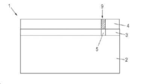
도 1은 박막 태양 전지들의 제조를 위한 중간 생성물인 층 구조의 도 2의 절단선 A-A를 따라 절단한 단면도이다.
도 2는 도 1의 층 구조의 평면도이다.
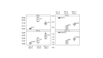
도 3은 2 개의 캐리어 기판들 및 하나의 위트니스글라스 (witness glass)를 갖는 흡수층의 다양한 원소들의 상대적 비율을 나타내기 위한 박스 플롯 (box plot) 이다.
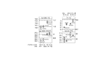
도 4는 측정 필드들이 있거나 없는 캐리어 기판들로 다양한 물리적 파라미터를 나타내기 위한 박스 플롯이다.
도 5는 흐름도를 사용하는 프로세스 단계들의 예시적인 실시예이다.The present invention is now described in detail using exemplary embodiments with reference to the accompanying drawings.
1 is a cross-sectional view taken along line AA of FIG. 2 of a layer structure that is an intermediate product for the production of thin film solar cells.
FIG. 2 is a plan view of the layer structure of FIG. 1.
FIG. 3 is a box plot for showing the relative proportions of various elements of the absorbent layer with two carrier substrates and one witness glass.
4 is a box plot for showing various physical parameters with carrier substrates with or without measurement fields.
5 is an exemplary embodiment of process steps using a flow chart.
먼저, 도 1 및 도 2를 고려하면, 본 발명에 따른 방법을 설명하기 위한 예시적인 층 구조(1)를 개략적으로 도시한다. 층 구조(1)는 직렬 연결되고 집적된 박막 태양 전지들의 생산에서 중간 생성물이다.Referring first to FIGS. 1 and 2, an exemplary layer structure 1 for describing the method according to the invention is schematically illustrated. The layer structure 1 is an intermediate product in the production of series connected and integrated thin film solar cells.
층 구조(1)는 기판(2)과 기판(2)상의 후면 전극층(3)을 포함한다. 측정층(4)은 후면 전극층(3) 상에 배치되는데, 이는 광활성 흡수층 또는 광활성 흡수층의 전구체 층이다.The layer structure 1 includes a
여기서 기판(2)은 예를 들어 무기 유리로 제조되는 반면, 박막 태양 전지들을 제조하는데 있어서 거치는 공정 단계에 대한 불활성 거동뿐만 아니라 만족스러운 안정성을 갖는 다른 절연 재료들이 마찬가지로 사용될 수 있다. 예를 들어 플라스틱, 특히 중합체 또는 금속 또는 금속 합금을 사용할 수 있다. 층 두께 및 특정 재료 특성에 따라, 기판(2)은 강성판 또는 가요성 필름으로 설계될 수 있다. 기판(2)의 층 두께는 예를 들어 1mm 내지 5mm 이다. 후면 전극층(3)은 광 입사에 대면하는 기판(2)의 표면 상에 배열된다. 후면 전극층(3)은, 예를 들어 빛이 침투할 수 없는 금속으로 이루어진다. 예를 들어, 금속은 기상 증착 또는 마그네트론 강화 음극 스퍼터링에 의해 기판(2) 상에 증착될 수 있다. 후면 전극층(3)은 예를 들어 구리(Cu) 및/또는 아연(Zn)을 포함하거나 이것으로 만들어지거나 이러한 금속을 갖는 다층 시스템으로 구성된다. 후면 전극층(3)의 층 두께는 예를 들어 1 ㎛ 미만이고 특히 300 nm 내지 600 nm의 범위이다. 패터닝 후, 박막 태양 전지들의 후면 접점은 후면 전극층(3)에 형성된다. 예를 들어 Si3N4, SiON 또는 SiCN으로 만들어진 알칼리 장벽은 기판(2)과 후면 전극층(3) 사이에 배치될 수 있다. 이것은 도 1에 도시되지 않았다.Here, the
측정층(4)은 예를 들어 광활성 흡수층이고, 바람직하게는 켈코파이라이트 화합물 반도체, 특히 Cu2ZnSn(S,Se)4, Cu(In,Ga,Al)(S,Se)2, CuInSe2, CuInS2, Cu (In,Ga)Se2 또는 Cu(In,Ga)(S,Se)2 또는 케스트라이트 화합물 반도체 (CZTS)를 포함하거나 이들로 만들어진다. 바람직하게는, 측정층(4)은 Cu(InGa)(S,Se)2를 포함하거나 이로 이루어지고, 예를 들어 전술한 2 단계 RTP 공정에 의해 제조되었다. 측정층(4)은 또한 흡수층 (선택적으로 다중층으로 구성됨)의 전구체 층일 수 있으며, 열처리에 의해 변환되어 화합물 반도체를 형성한다. 측정층(4)은 후면 전극층(3) 상에 직접 도포된다. 측정층(4)은 예를 들어 1.5 ㎛의 두께를 갖는다.The measuring layer 4 is, for example, a photoactive absorbing layer, preferably a kelcopyrite compound semiconductor, in particular Cu 2 ZnSn(S,Se) 4 , Cu(In,Ga,Al)(S,Se) 2 , CuInSe 2 , CuInS 2 , Cu (In,Ga)Se 2 or Cu(In,Ga)(S,Se) 2 or castrite compound semiconductor (CZTS). Preferably, the measurement layer 4 comprises or consists of Cu(InGa)(S,Se) 2 , and has been prepared, for example, by the two-step RTP process described above. The measurement layer 4 may also be a precursor layer of an absorbing layer (optionally composed of multiple layers), which is converted by heat treatment to form a compound semiconductor. The measurement layer 4 is applied directly on the
전형적으로, 예를 들어 도핑되지 않은 산화 아연 (i-ZnO)을 포함하는 적어도 하나의 버퍼층 (도시되지 않음)이 측정층(4) 상에 배열된다. 그 위에는 전면 전극층 (도시되지 않음)이 위치한다. 전면 전극층은 가시 광선 스펙트럼 범위에서 방사선에 투명하고, 패터닝 후에 그것에는 박막 태양 전지의 전면 접점이 형성된다. 일반적으로, 환경 영향으로부터 보호하기 위한 커버층 (도시되지 않음)이 전면 전극위 도포되며, 전면 전극은 예를 들어 폴리비닐부티랄 (PVB), 에틸렌 비닐 아세테이트 (EVA), 또는 실리콘으로 만들어진 플라스틱 층 (봉지 필름)으로 만들어진다 . 또한, 햇빛에 투명한 커버 플레이트 (도시되지 않음)가 마련될 수있다. 직렬 연결되고 집적된 박막 태양 전지들의 제조를 위해, 후면 전극층 (3) 및 전면 전극층 (도시되지 않음)이 라인 P1, P2 및 P3 (후면 전극층을 분할하기 위한 P1, 전면 전극섹션과 후면 전극섹션의 접촉을 위한 P2, 전면 전극층을 분리하기 위한 P3) 을 패터닝함으로써 자체 공지 된 방식으로 패터닝된다.Typically, at least one buffer layer (not shown) comprising, for example, undoped zinc oxide (i-ZnO) is arranged on the measuring layer 4. Above it is a front electrode layer (not shown). The front electrode layer is transparent to radiation in the visible light spectrum range, and after patterning it forms the front contact of the thin film solar cell. Generally, a cover layer (not shown) for protection from environmental influences is applied on the front electrode, the front electrode being a plastic layer made of, for example, polyvinyl butyral (PVB), ethylene vinyl acetate (EVA), or silicone It is made of (envelope film). In addition, a cover plate (not shown) that is transparent to sunlight can be provided. For the production of series-connected and integrated thin film solar cells, the
중간 생성물이 도 1 및 도 2에 도시된, 박막 태양 전지들을 제조하기 위한 층 구조는 당업자에게 널리 공지되어 있으며, 이미 특허 문헌의 수많은 공보에, 예를 들어, DE 19956735 B4에 상세하게 기술되어있다. The layer structure for making thin film solar cells, with the intermediate product shown in FIGS. 1 and 2, is well known to those skilled in the art and has already been described in detail in numerous publications in the patent literature, for example DE 19956735 B4. .
도 1에 도시된 기판 구성에서, 후면 전극층(3)은 기판 (2)에 인접한다. 물론, 층 구조(1)는 기판 (2)이 투명하고 광의 진입면 위에 배치되는 상위기판구성 (superstrate configuration)을 가질 수 있다. In the substrate configuration shown in Fig. 1, the
예를 들어, 캐리어 기판 (2)은 인라인 생산 시스템에서 후면 전극층 (3) 및 측정층 (4)으로 코팅되며, 캐리어 기판 (2)은 이러한 목적을 위해 도 2에서 화살표로 표시된 이송 방향 (T)을 따라 이동된다. 측정층 (4)이 흡수층의 전구체 층인 경우, 측정층 (4)은 흡수층으로 열적 변환된다.For example, the
도 2에서 알 수 있는 바와 같이, 캐리어 기판 (2)은 더 긴 치수 (a)와 더 짧은 치수 (b)를 갖는 직사각형이며, 예를 들어 더 긴 치수 (a)는 이송 방향 (T)으로 연장된다. 캐리어 기판 (2)의 표면이 후면 전극층 (3) 및 측정층 (4)으로 완전히 코팅되고, 즉 후면 전극층 (3)이 캐리어 기판 (2)을 완전히 덮고, 측정층 (4)은 후면 전극층 (3)을 완전히 덮는다. 도 2에 도시된 가상의 분리선 (6)에 의해, 광전 에너지 생성을 위해 제공된 박막 태양 전지들의 광활성 영역 (7)은 에지 영역 (8)에서 분리되고, 여기서 캐리어 기판 (2)은 나중에 완전히 디코팅된다 (decoated). 도 1 및 도 2에 도시된 박막 태양 전지들을 제조시의 중간 생성물에서, 후면 전극층 (3) 및 측정층 (4)은 광활성 영역 (7) 및 에지 영역 (8) 모두에 존재한다.As can be seen in Figure 2, the
층 구조 (1)에서, 후면 전극층 (3)은 각각의 경우 후면 전극층 (3)의 리세스 (불연속) 형태로 구현되는, 후면전극층이없는 복수의 영역들 (5)을 갖는다. 따라서 후면전극층이없는 영역들 (5)은 각각의 경우 후면 전극층 (3)의 외부 경계 내에 위치하고 각각의 경우에 후면 전극층 (3)의 재료로 둘러싸여 있다. 후면전극층이없는 영역들 (5)은, 예를 들어, 다른 형상이 마찬가지로 가능한, 직사각형 형상을 갖는다. 측정층 (4)은 모든 후면전극층이없는 영역 (5)들을 덮는다.In the layer structure (1), the back electrode layer (3) has a plurality of regions (5) without a back electrode layer, each implemented in the form of a recess (discontinuous) of the back electrode layer (3). Therefore, the
도 2에 도시된 바와 같이, 선택적으로 존재할 수 있는, 후면전극층이없는 복수의 영역들 (5)이 후면 전극층 (3)에 구현된다. 예를 들어, 후면전극층이없는 복수의 영역들 (5)이 (나중에) 광학적으로 활성화된 영역 (7) 및 / 또는 (나중에) 디코팅된 에지 영역 (8)에 구현된다. 후면전극층이없는 영역들 (5)은 예를 들어 캐리어 기판의 이송 방향 (T)에 대해 횡 방향으로, 즉, 예를 들어, 여기서는, 캐리어 기판 (2)의 짧은 치수 (b)를 따라서 및/또는 캐리어 기판 (2)의 이송 방향 (T)을 따라, 즉, 예를 들어, 여기서는 캐리어 기판의 보다 긴 치수 (a)를 따라서 배열된다.As shown in Fig. 2, a plurality of
후면전극층이없는 영역들 (5)은 각각의 경우 후면 전극층 (3)을 바람직하게는 1 내지 1000 피코 초 범위의 펄스 지속 시간을 갖는 펄스 레이저 빔 (레이저 어블레이션)에 의해 디코팅함으로써 생성된다.The
후면전극층이없는 각 영역 (5)위에 이하 "측정 필드"(9)로 지칭되는 측정층 (4)의 영역이 위치하며, 측정층 (4)의 하나 또는 복수의 원소들의 양 또는 함량 (상대적 값)을 측정 필드 (9)에서만 측정한다. 도 1에서, 측정층 (4)의 측정 필드 (9)는 해칭 (hatching)으로 식별된다.Above each region (5) without the back electrode layer is the region of the measurement layer (4), hereinafter referred to as the "measurement field" (9), where the amount or content of one or more elements of the measurement layer (4) (relative value) ) Is measured only in the measurement field (9). In FIG. 1, the measurement field 9 of the measurement layer 4 is identified as hatching.
도 1 및 도 2의 층 구조 (1)의 제조는 도 5의 흐름도를 참조하여 예시된 바와 같이 본 발명에 따른 방법의 일부이다. 따라서, 먼저 캐리어 기판 (2)이 준비된다 (단계 I). 그 후, 후면 전극층 (3)이 캐리어 기판 (2) 상에 도포된다 (단계 II). 이어서, 후면 전극층 (3)에서 후면전극층이없는 영역 (5)을 형성하고 (단계 III), 측정층 (4)을 만든다 (단계 IV). 그 후, 측정층 (4)의 적어도 하나의 성분 (원소)의 양 또는 상대적 함량은 각각의 경우 후면전극층이없는 영역 (5) 위에 위치한 측정층 (4)의 측정 필드들 (9)에서 결정된다 (단계 V). 이러한 측정은 측정 필드들 외부에서 발생하지 않는다.The production of the layer structure 1 of FIGS. 1 and 2 is part of the method according to the invention as illustrated with reference to the flowchart of FIG. 5. Therefore, the
특히, 단계 V에서, 측정층 (4)의 정확한 조성, 예를 들어 원소 Cu, In 및 Ga의 양 또는 함량이 결정된다. 이는 예를 들어, 후면 전극층 (3)에 Cu가 포함되어 있더라도 매우 정확하게 측정된다. 예를 들어, 바람직하게는 X-선 방사선 조사를 통한 여기 (excitation)가 수행되는 파장분산 X-선 분광법 (WDX) 또는 에너지분산 X-선 분광법 (EDX)이 사용된다. 후면 전극층에 존재하는 동일 원소에 의해서 측정층 (4)의 하나의 원소에 대한 측정 신호 왜곡 또는 간섭은 후면전극층이없는 영역들 (5) 위의 측정 필드들 (9)에서만 독점적으로 측정하는 것에 의해 유리하게 회피될 수 있다.In particular, in step V, the exact composition of the measuring layer 4, for example the amount or content of elements Cu, In and Ga, is determined. This is measured very accurately even if Cu is contained in the
도 3은 다양한 시편의 전구체 층에서 다양한 원소의 백분율 몫을 비교하기 위한 박스 플롯 (box plot)을 도시한다. 전구체 층 및 누락된 후면 전극층을 갖는 위트니스글라스 (witness glass) 및 구리 (Cu)를 함유하는 후면 전극층을 갖는 캐리어 기판상의 측정 필드에서 측정을 수행하였으며, 여기서 측정 필드 아래에서 두 개의 서로 다른 레이저 (피코 초 레이저 및 나노초 레이저)로 후면 전극층을 제거 하였다 . 왼쪽 도면은 다양한 시편에 대한 In 및 Ga의 백분율 점유율 (원자 %)을 기록한다. 오른쪽 도면은 다양한 시편에 대한 Cu의 백분율 점유율 (원자 %)과 Cu/(In+Ga) 비율을 기록한다. WDX X-선 분광법으로 측정하였다.3 shows a box plot for comparing percentage quotients of various elements in precursor layers of various specimens. Measurements were performed in a measurement field on a carrier substrate with a back electrode layer containing witness glass and copper (Cu) with a precursor layer and a missing back electrode layer, where two different lasers (pico Ultra-laser and nano-second laser) to remove the back electrode layer. The figure on the left reports the percentage occupancy (in atomic %) of In and Ga for various specimens. The figure on the right records the percentage occupancy (% atomic) and Cu/(In+Ga) ratio of Cu for various specimens. It was measured by WDX X-ray spectroscopy.
명백히, ps 레이저에 의해 후면 전극층이 제거된 측정 필드에서의 Cu/(In+Ga) 비는 위트니스글라스 (witness glass)에 대해 측정된 값에 가깝다. 대조적으로, ns 레이저로 처리된 측정 필드에서, 여전히 존재하는 Cu 잔류물로 인해 그 비율이 상당히 높다. 따라서, 본 실험에 사용된 ps 레이저는 Cu/(In+Ga) 비를 정확하게 결정하는 데에 특히 적합한 반면, ns 레이저의 레이저 유도는 예를 들어 더 높은 펄스 대 펄스 중첩 또는 더 높은 전력에 의해 최적화 될 수있다. 그러나, 원칙적으로 ns 레이저도 적합하다. Cu/(In+Ga) 비는 ps 레이저 공정에 대해 1 %의 편차를 가지며, ns 레이저 공정에 대해서는 위트니스글라스 (witness glass)에 대해 측정된 값에서 2%의 편차를 갖는다. 이것의 원인은 아마도 ns 공정에서 Cu의 잔류물이 비교적 높기 때문일 것 이다. 레이저 프로세스의 조정을 통해 여기서도 여전히 상당한 개선이 달성될 것으로 예상된다. ps 레이저 공정의 경우, Cu 값들과 측정된 Cu/(In-Ga) 비율은, 대조적으로, 위트니스글라스 (witness glasses)의 값보다 약간 낮고, 이는 디코팅이 적절하게 되었다는 것을 확인해주는 것이다.Obviously, the Cu/(In+Ga) ratio in the measurement field where the back electrode layer was removed by the ps laser is close to the value measured for witness glass. In contrast, in the measurement field treated with an ns laser, the proportion is quite high due to the Cu residue still present. Thus, the ps laser used in this experiment is particularly suitable for accurately determining the Cu/(In+Ga) ratio, while the laser induction of the ns laser is optimized, for example, by higher pulse to pulse overlap or higher power Can be However, in principle, an ns laser is also suitable. The Cu/(In+Ga) ratio has a deviation of 1% for the ps laser process, and a deviation of 2% from the measured value for witness glass for the ns laser process. This is probably due to the relatively high residual of Cu in the ns process. It is expected that significant improvements will still be achieved here through adjustment of the laser process. In the case of the ps laser process, the Cu values and the measured Cu/(In-Ga) ratio, in contrast, are slightly lower than the value of the witness glasses, which confirms that the decoating has become appropriate.
상기 결과들은 국부적인 저항 손실 (ohmic losses)을 나타내는 시편에 대한 로크인 적외선분석 (lock-in-infrared-analyses)에 의해 추가적으로 지지되었다. 여기서는 측정 필드들이 비활동 영역으로 인식될 수 있었지만 저항 손실이 증가하지 않았다.The results were further supported by lock-in-infrared-analyses on specimens showing local ohmic losses. Here, the measurement fields could be recognized as inactive areas, but the resistance loss did not increase.
측정층은 측정 필드들의 영역에서 현미경으로 추가로 분석되었다. 이들 영역들에서, 일부 성장 결함 및 최소 미세 스폴링 (spalling)이 확실하게 식별가능 하고, 그것들은 각각의 경우에 사용된 레이저 방법에 따라 좌우되었다. 그러나, 이들 영역들은 전기적으로, 적어도 광학 현미경 하에서는 중대해 보이지 않았다. 왜냐하면 그 영역들은 최종 모듈에서 전면 및 후면 전극 사이에 도전성 연결을 해서 부분적 단락을 초래할 수 없는 영역들에 위치하여 있기 때문이다. 적외선 분석으로 이 평가를 확인했다.The measurement layer was further analyzed microscopically in the area of the measurement fields. In these areas, some growth defects and minimal fine spalling are reliably discernible, and they depend on the laser method used in each case. However, these areas did not look great electrically, at least under an optical microscope. This is because the regions are located in regions where a conductive connection between the front and rear electrodes in the final module cannot result in a partial short circuit. Infrared analysis confirmed this evaluation.
본 발명에 따른 방법이 나중에 광학적으로 비활성인 박막 태양 모듈의 영역에서뿐만 아니라 광활성 영역에서도 사용될 수 있다는 것이 실험으로 나타나고 있다. It has been shown experimentally that the method according to the invention can later be used in the photoactive region as well as in the region of the optically inert thin film solar module.
도 4는 Cu를 함유하는 박막 태양 전지 후면 전극을 갖는 캐리어 기판 상에 측정 필드를 갖거나 갖지 않는 박막 태양 모듈의 IU 특성을 도시한다. 다수의 박막 태양 전지들 내에서, 후면 전극은 2 개의 상이한 레이저로 광활성 영역에서 제거되었다. 각각의 경우에, 30 x 30 cm2 캐리어 기판이 측정 필드를 갖거나 갖지 않은 채로 광활성 영역에 만들어졌다. 효율 (Eta), 단락 전류 밀도 (ISC), 모듈에서 태양 전지당 개방 회로 전압 (Voc) 및 충전 계수 (FF)의 측정값에 대한 박스 플롯이 도시되어 있다. 캡슐화 ("회로")뿐만 아니라 캡슐화 및 광노화후 ("LS후 모듈") 박막 태양 모듈간에 차이가 있다. 측정 필드의 존재 ("예") 또는 측정 필드의 부재 ("아니오")에 따라 추가 구별이 이루어진다. 박스 플롯의 유의 막대(significance bar)들은,이 경우에 여러 측정 필드가 실제로 비교적 작은 영역에서 만들어졌더라도, 효율에 대한 측정 필드의 실질적인 영향이 없음을 보여 주고 있다. 따라서 모듈 면적이 약 1m2 인 일반 제품에 미치는 영향은 무시할 수 있다. 4 shows the IU properties of a thin film solar module with or without a measurement field on a carrier substrate having a thin film solar cell back electrode containing Cu. In many thin film solar cells, the back electrode was removed in the photoactive region with two different lasers. In each case, a 30 x 30 cm 2 carrier substrate was created in the photoactive region with or without a measurement field. Box plots for measurements of efficiency (Eta), short-circuit current density (ISC), open circuit voltage (Voc) and charge factor (FF) per solar cell in the module are shown. There is a difference between thin film solar modules after encapsulation ("circuit") as well as after encapsulation and photoaging ("post-LS module"). Further distinctions are made depending on the presence of the measurement field (“Yes”) or the absence of the measurement field (“No”). Significance bars in the box plot show that even though several measurement fields in this case are actually made in relatively small areas, there is no real effect of the measurement field on efficiency. Therefore, the effect on the general product with a module area of about 1 m 2 can be neglected.
상기 설명으로부터, 본 발명에 의해 흡수층 또는 이의 전구체 층의 조성을 제어하기 위한 종래 기술 방법의 단점이 극복될 수 있음이 명백해졌다. 측정층의 원소들이 후면 전극층의 신호 왜곡 없이 후면전극층이없는 영역들을 통해 신뢰성 있고 확실하게 검증될 수 있다. 후면전극층이없는 영역들이 박막 태양 모듈의 광활성 영역 내에 있을 때 박막 태양 모듈의 품질 자체는 실질적으로 손상되지 않는다. 적어도 WDX 또는 EDX X-선 분광법을 사용하여 측정한 경우, 후면전극층이없는 영역들에서 잔류물 존재의 영향은 무시할 만하다. 잔류물 존재 신호는 후면전극층이없는 영역들 위에 놓인 측정층에 의해 감쇠된다는 것이 추가적으로 밝혀진 사실이다. 후면전극층이없는 영역들에서는 전구체 층 또는 열 변환에 의해 생성된 흡수층의 접착력이 저하되는 문제점이 관찰되지 않았다. 마찬가지로, 예를 들어 실리콘 질화물 (SiN)로 만들어지고 캐리어 기판 상에 위치된 배리어 층은 후면전극층이없는 영역들에서 전구체 층 또는 흡수층의 성장에 불리한 영향을 미치는 것이 관찰되지 않았다. 결과적으로, 본 발명에 따른 방법은 박막 태양 전지들의 제조에 유리하게 사용될 수 있다. From the above description, it has become apparent that the disadvantages of the prior art method for controlling the composition of the absorber layer or its precursor layer can be overcome by the present invention. The elements of the measurement layer can be reliably and reliably verified through regions without the back electrode layer without signal distortion of the back electrode layer. When the regions without the back electrode layer are within the photoactive region of the thin film solar module, the quality of the thin film solar module itself is not substantially damaged. At least when measured using WDX or EDX X-ray spectroscopy, the effect of the presence of residue in the areas without the back electrode layer is negligible. It is further found that the residual presence signal is attenuated by the measurement layer overlying the areas without the back electrode layer. In regions without a back electrode layer, no problem was observed in that the adhesion strength of the precursor layer or the absorber layer generated by heat conversion was lowered. Likewise, a barrier layer made of, for example, silicon nitride (SiN) and positioned on a carrier substrate was not observed to adversely affect the growth of the precursor layer or absorber layer in regions without the back electrode layer. Consequently, the method according to the invention can be advantageously used in the manufacture of thin film solar cells.
1
층 구조
2
캐리어 기판
3
후면 전극층
4
측정층
5
후면전극이없는 영역
6
분리선
7
광전 영역
8
에지 영역
9
측정 필드1-layer structure
2 carrier substrate
3 back electrode layer
4 Measurement layer
5 Area without back electrode
6 Separator
7 photoelectric area
8 edge area
9 Measurement field
Claims (15)
-캐리어 기판 (2)을 제공하는 단계,
-캐리어 기판 (2) 상에 후면 전극층 (3)을 증착하는 단계,
-적어도 하나의 후면전극층이없는 영역 (5)을 생성하는 단계,
-측정층 (4)이 상기 적어도 하나의 후면전극층이없는 영역 (5) 위에 위치하도록 상기 후면 전극층 (3) 위에 측정층 (4)을 생성하는 단계-여기서 측정층 (4)은 광활성 흡수층 (4) 또는 광활성 흡수층 (4)의 전구체 층이고-,
-상기 후면 전극층 (3)의 상기 적어도 하나의 후면전극층이없는 영역 (5) 위에 위치한 상기 측정층 (4)의 영역 (9)에서 상기 측정층 (4)의 적어도 하나의 성분의 양 또는 상대적인 비율을 결정하는 단계를 포함하는, 제조 방법.A method of manufacturing a layer structure (1) for producing thin film solar cells,
-Providing a carrier substrate (2),
-Depositing the back electrode layer (3) on the carrier substrate (2),
-Creating an area 5 without at least one back electrode layer,
-Creating a measurement layer (4) over the back electrode layer (3) such that the measurement layer (4) is located over the region (5) without the at least one back electrode layer-where the measurement layer (4) is a photoactive absorbing layer (4 ) Or a precursor layer of the photoactive absorbing layer (4)-,
-The amount or relative proportion of at least one component of the measuring layer 4 in the region 9 of the measuring layer 4 located above the region 5 without the at least one rear electrode layer of the rear electrode layer 3 The method comprising the step of determining.
A thin film solar module manufactured using the method according to any one of claims 1 to 14.
Applications Claiming Priority (3)
| Application Number | Priority Date | Filing Date | Title |
|---|---|---|---|
| EP17166982 | 2017-04-19 | ||
| EP17166982.3 | 2017-04-19 | ||
| PCT/CN2018/083473 WO2018192512A1 (en) | 2017-04-19 | 2018-04-18 | Method for producing layer structure for thin-film solar cells |
Publications (2)
| Publication Number | Publication Date |
|---|---|
| KR20200094084A true KR20200094084A (en) | 2020-08-06 |
| KR102352100B1 KR102352100B1 (en) | 2022-01-14 |
Family
ID=58578883
Family Applications (1)
| Application Number | Title | Priority Date | Filing Date |
|---|---|---|---|
| KR1020197032274A Active KR102352100B1 (en) | 2017-04-19 | 2018-04-18 | Method for producing layered structures for thin-film solar cells |
Country Status (6)
| Country | Link |
|---|---|
| US (1) | US11183605B2 (en) |
| EP (1) | EP3613083B1 (en) |
| JP (1) | JP7070946B2 (en) |
| KR (1) | KR102352100B1 (en) |
| CN (1) | CN111279491B (en) |
| WO (1) | WO2018192512A1 (en) |
Citations (4)
| Publication number | Priority date | Publication date | Assignee | Title |
|---|---|---|---|---|
| JP2013115128A (en) * | 2011-11-25 | 2013-06-10 | Showa Shell Sekiyu Kk | Thin film solar cell module and method of manufacturing the same |
| KR20130129923A (en) * | 2010-10-20 | 2013-11-29 | 아사히 가라스 가부시키가이샤 | Glass substrate for cu-in-ga-se solar cells and solar cell using same |
| JP2014090014A (en) * | 2012-10-29 | 2014-05-15 | Fujifilm Corp | Method and device for forming compound thin film |
| US20150228820A1 (en) * | 2014-02-07 | 2015-08-13 | Tsmc Solar Ltd. | Front contact for a solar cell, and method of making same |
Family Cites Families (26)
| Publication number | Priority date | Publication date | Assignee | Title |
|---|---|---|---|---|
| JPH01125875A (en) * | 1988-10-19 | 1989-05-18 | Matsushita Electric Ind Co Ltd | Solar cell element |
| CA2024662A1 (en) * | 1989-09-08 | 1991-03-09 | Robert Oswald | Monolithic series and parallel connected photovoltaic module |
| DE4442824C1 (en) | 1994-12-01 | 1996-01-25 | Siemens Ag | Solar cell having higher degree of activity |
| DE19956735B4 (en) | 1999-11-25 | 2008-08-21 | Shell Erneuerbare Energien Gmbh | A thin film solar cell comprising a chalcopyrite compound and a titanium and oxygen-containing compound |
| SE0400582D0 (en) * | 2004-03-05 | 2004-03-05 | Forskarpatent I Uppsala Ab | Method for in-line process control of the CIGS process |
| US20090104342A1 (en) * | 2007-10-22 | 2009-04-23 | Applied Materials, Inc. | Photovoltaic fabrication process monitoring and control using diagnostic devices |
| EP2159846A1 (en) * | 2008-08-29 | 2010-03-03 | ODERSUN Aktiengesellschaft | Thin film solar cell and photovoltaic string assembly |
| JP5297840B2 (en) * | 2009-03-03 | 2013-09-25 | シャープ株式会社 | LAMINATE, THIN-FILM PHOTOELECTRIC CONVERSION DEVICE, INTEGRATED THIN-FILM SOLAR CELL AND METHOD FOR PRODUCING THEM |
| EP2416377B1 (en) * | 2009-03-31 | 2015-07-01 | LG Innotek Co., Ltd. | Solar cell and manufacturing method thereof |
| KR20110008640A (en) * | 2009-07-20 | 2011-01-27 | 삼성전자주식회사 | Solar cell module and manufacturing method thereof |
| KR101144570B1 (en) * | 2009-09-30 | 2012-05-11 | 엘지이노텍 주식회사 | Solar cell and method of fabircating the same |
| US8969720B2 (en) * | 2010-03-17 | 2015-03-03 | Dow Global Technologies Llc | Photoelectronically active, chalcogen-based thin film structures incorporating tie layers |
| JP5430748B2 (en) * | 2010-04-14 | 2014-03-05 | 京セラ株式会社 | Photoelectric conversion device and method for manufacturing photoelectric conversion device |
| JP5054157B2 (en) * | 2010-06-17 | 2012-10-24 | 昭和シェル石油株式会社 | CIS thin film solar cell |
| KR20120086447A (en) * | 2011-01-26 | 2012-08-03 | 엘지이노텍 주식회사 | Solar cell apparatus and method of fabricating the same |
| WO2013031453A1 (en) * | 2011-08-29 | 2013-03-07 | 京セラ株式会社 | Photoelectric conversion apparatus |
| KR20130028449A (en) * | 2011-09-09 | 2013-03-19 | 한국철강 주식회사 | Thin film type solar cells and manufacturing method thereof |
| US20130118569A1 (en) * | 2011-11-14 | 2013-05-16 | Taiwan Semiconductor Manufacturing Co., Ltd. | Method for forming thin film solar cell with buffer-free fabrication process |
| US20130186461A1 (en) * | 2012-01-20 | 2013-07-25 | Dong-jin Kim | Solar cell and method of manufacturing the same |
| US9224903B2 (en) * | 2012-04-17 | 2015-12-29 | Kyocera Corporation | Method for manufacturing photoelectric converter |
| CN104396015A (en) * | 2012-05-03 | 2015-03-04 | 内克西斯公司 | Laser etching a stack of thin layers for a connection of a photovoltaic cell |
| US9343378B2 (en) * | 2013-03-12 | 2016-05-17 | Alliance For Sustainable Energy, Llc | Optical control of multi-stage thin film solar cell production |
| CN103227243B (en) * | 2013-05-06 | 2015-08-05 | 王家雄 | Prepare the volume to volume production method of copper-indium-galliun-selenium film solar cell |
| KR20150031889A (en) | 2013-09-17 | 2015-03-25 | 엘지이노텍 주식회사 | Solar cell |
| KR20150039536A (en) | 2013-10-02 | 2015-04-10 | 엘지이노텍 주식회사 | Solar cell |
| EP2887405A1 (en) * | 2013-12-23 | 2015-06-24 | Saint-Gobain Glass France | Coating system for thin film solar cells |
-
2018
- 2018-04-18 EP EP18787592.7A patent/EP3613083B1/en active Active
- 2018-04-18 KR KR1020197032274A patent/KR102352100B1/en active Active
- 2018-04-18 JP JP2020507732A patent/JP7070946B2/en active Active
- 2018-04-18 CN CN201880040964.5A patent/CN111279491B/en active Active
- 2018-04-18 WO PCT/CN2018/083473 patent/WO2018192512A1/en not_active Ceased
- 2018-04-18 US US16/605,793 patent/US11183605B2/en active Active
Patent Citations (4)
| Publication number | Priority date | Publication date | Assignee | Title |
|---|---|---|---|---|
| KR20130129923A (en) * | 2010-10-20 | 2013-11-29 | 아사히 가라스 가부시키가이샤 | Glass substrate for cu-in-ga-se solar cells and solar cell using same |
| JP2013115128A (en) * | 2011-11-25 | 2013-06-10 | Showa Shell Sekiyu Kk | Thin film solar cell module and method of manufacturing the same |
| JP2014090014A (en) * | 2012-10-29 | 2014-05-15 | Fujifilm Corp | Method and device for forming compound thin film |
| US20150228820A1 (en) * | 2014-02-07 | 2015-08-13 | Tsmc Solar Ltd. | Front contact for a solar cell, and method of making same |
Also Published As
| Publication number | Publication date |
|---|---|
| JP2020518137A (en) | 2020-06-18 |
| JP7070946B2 (en) | 2022-05-18 |
| EP3613083A4 (en) | 2021-01-06 |
| US11183605B2 (en) | 2021-11-23 |
| KR102352100B1 (en) | 2022-01-14 |
| CN111279491A (en) | 2020-06-12 |
| WO2018192512A1 (en) | 2018-10-25 |
| EP3613083C0 (en) | 2026-02-25 |
| EP3613083B1 (en) | 2026-02-25 |
| CN111279491B (en) | 2022-05-31 |
| US20200052138A1 (en) | 2020-02-13 |
| EP3613083A1 (en) | 2020-02-26 |
Similar Documents
| Publication | Publication Date | Title |
|---|---|---|
| US8309390B2 (en) | Method of manufacturing a photovoltaic device and system for patterning an object | |
| TWI478367B (en) | Solar cell and method of manufacturing same | |
| Gouillart et al. | Interface engineering of ultrathin Cu (In, Ga) Se2 solar cells on reflective back contacts | |
| CN102744520A (en) | Methods of temporally varying the laser intensity during scribing a photovoltaic device | |
| US11211508B2 (en) | Thin-film solar module with improved shunt resistance | |
| ES2978384T3 (en) | Method for post-treatment of an absorbent layer | |
| CN102290456A (en) | Method of modifying a cadmium telluride layer, and a thin film device having a cadmium telluride layer | |
| JP6297038B2 (en) | Thin film solar cell and method for manufacturing thin film solar cell | |
| JP2013149697A (en) | Integrated soar cell manufacturing method | |
| US11444217B2 (en) | Method for producing a thin-film solar module | |
| KR102352100B1 (en) | Method for producing layered structures for thin-film solar cells | |
| EP2811537A2 (en) | Photoelectric module and method of manufacturing the same | |
| CN102315321A (en) | Transparency conducting layer and forming method thereof | |
| JP2019009241A (en) | Solar cell and method for manufacturing the same | |
| KR101326964B1 (en) | Solar cell module and method of fabricating the same | |
| KR101768788B1 (en) | Method for producing a compound semiconductor, and thin-film solar cell | |
| JP2015162525A (en) | Photoelectric conversion element, solar cell, and method for manufacturing photoelectric conversion element | |
| JP2021174868A (en) | Manufacturing method of photoelectric conversion element | |
| JP2019029629A (en) | Solar cell and method for manufacturing the same | |
| KR20150082978A (en) | Solar cell and method of fabricating the same | |
| CN105706247A (en) | Rear contact substrate for photovoltaic cell |
Legal Events
| Date | Code | Title | Description |
|---|---|---|---|
| PA0105 | International application |
St.27 status event code: A-0-1-A10-A15-nap-PA0105 |
|
| PA0201 | Request for examination |
St.27 status event code: A-1-2-D10-D11-exm-PA0201 |
|
| T11-X000 | Administrative time limit extension requested |
St.27 status event code: U-3-3-T10-T11-oth-X000 |
|
| T11-X000 | Administrative time limit extension requested |
St.27 status event code: U-3-3-T10-T11-oth-X000 |
|
| T11-X000 | Administrative time limit extension requested |
St.27 status event code: U-3-3-T10-T11-oth-X000 |
|
| R18-X000 | Changes to party contact information recorded |
St.27 status event code: A-3-3-R10-R18-oth-X000 |
|
| T11-X000 | Administrative time limit extension requested |
St.27 status event code: U-3-3-T10-T11-oth-X000 |
|
| N231 | Notification of change of applicant | ||
| P11-X000 | Amendment of application requested |
St.27 status event code: A-2-2-P10-P11-nap-X000 |
|
| P13-X000 | Application amended |
St.27 status event code: A-2-2-P10-P13-nap-X000 |
|
| PN2301 | Change of applicant |
St.27 status event code: A-3-3-R10-R13-asn-PN2301 St.27 status event code: A-3-3-R10-R11-asn-PN2301 |
|
| PG1501 | Laying open of application |
St.27 status event code: A-1-1-Q10-Q12-nap-PG1501 |
|
| D13-X000 | Search requested |
St.27 status event code: A-1-2-D10-D13-srh-X000 |
|
| D14-X000 | Search report completed |
St.27 status event code: A-1-2-D10-D14-srh-X000 |
|
| E902 | Notification of reason for refusal | ||
| PE0902 | Notice of grounds for rejection |
St.27 status event code: A-1-2-D10-D21-exm-PE0902 |
|
| T11-X000 | Administrative time limit extension requested |
St.27 status event code: U-3-3-T10-T11-oth-X000 |
|
| R17-X000 | Change to representative recorded |
St.27 status event code: A-3-3-R10-R17-oth-X000 |
|
| P11-X000 | Amendment of application requested |
St.27 status event code: A-2-2-P10-P11-nap-X000 |
|
| P13-X000 | Application amended |
St.27 status event code: A-2-2-P10-P13-nap-X000 |
|
| E701 | Decision to grant or registration of patent right | ||
| PE0701 | Decision of registration |
St.27 status event code: A-1-2-D10-D22-exm-PE0701 |
|
| GRNT | Written decision to grant | ||
| PR0701 | Registration of establishment |
St.27 status event code: A-2-4-F10-F11-exm-PR0701 |
|
| PR1002 | Payment of registration fee |
St.27 status event code: A-2-2-U10-U12-oth-PR1002 Fee payment year number: 1 |
|
| PG1601 | Publication of registration |
St.27 status event code: A-4-4-Q10-Q13-nap-PG1601 |
|
| PN2301 | Change of applicant |
St.27 status event code: A-5-5-R10-R13-asn-PN2301 St.27 status event code: A-5-5-R10-R11-asn-PN2301 |
|
| P22-X000 | Classification modified |
St.27 status event code: A-4-4-P10-P22-nap-X000 |
|
| PR1001 | Payment of annual fee |
St.27 status event code: A-4-4-U10-U11-oth-PR1001 Fee payment year number: 4 |
|
| P22-X000 | Classification modified |
St.27 status event code: A-4-4-P10-P22-nap-X000 |