KR20200095103A - 데이터 저장 장치 및 그 동작 방법 - Google Patents
데이터 저장 장치 및 그 동작 방법 Download PDFInfo
- Publication number
- KR20200095103A KR20200095103A KR1020190012769A KR20190012769A KR20200095103A KR 20200095103 A KR20200095103 A KR 20200095103A KR 1020190012769 A KR1020190012769 A KR 1020190012769A KR 20190012769 A KR20190012769 A KR 20190012769A KR 20200095103 A KR20200095103 A KR 20200095103A
- Authority
- KR
- South Korea
- Prior art keywords
- core
- mapping
- logical block
- cpu
- cores
- Prior art date
- Legal status (The legal status is an assumption and is not a legal conclusion. Google has not performed a legal analysis and makes no representation as to the accuracy of the status listed.)
- Granted
Links
Images


Classifications
-
- G—PHYSICS
- G06—COMPUTING OR CALCULATING; COUNTING
- G06F—ELECTRIC DIGITAL DATA PROCESSING
- G06F3/00—Input arrangements for transferring data to be processed into a form capable of being handled by the computer; Output arrangements for transferring data from processing unit to output unit, e.g. interface arrangements
- G06F3/06—Digital input from, or digital output to, record carriers, e.g. RAID, emulated record carriers or networked record carriers
- G06F3/0601—Interfaces specially adapted for storage systems
- G06F3/0628—Interfaces specially adapted for storage systems making use of a particular technique
- G06F3/0629—Configuration or reconfiguration of storage systems
- G06F3/0631—Configuration or reconfiguration of storage systems by allocating resources to storage systems
-
- G—PHYSICS
- G06—COMPUTING OR CALCULATING; COUNTING
- G06F—ELECTRIC DIGITAL DATA PROCESSING
- G06F3/00—Input arrangements for transferring data to be processed into a form capable of being handled by the computer; Output arrangements for transferring data from processing unit to output unit, e.g. interface arrangements
- G06F3/06—Digital input from, or digital output to, record carriers, e.g. RAID, emulated record carriers or networked record carriers
- G06F3/0601—Interfaces specially adapted for storage systems
- G06F3/0602—Interfaces specially adapted for storage systems specifically adapted to achieve a particular effect
- G06F3/061—Improving I/O performance
-
- G—PHYSICS
- G06—COMPUTING OR CALCULATING; COUNTING
- G06F—ELECTRIC DIGITAL DATA PROCESSING
- G06F12/00—Accessing, addressing or allocating within memory systems or architectures
- G06F12/02—Addressing or allocation; Relocation
- G06F12/0223—User address space allocation, e.g. contiguous or non contiguous base addressing
- G06F12/023—Free address space management
- G06F12/0238—Memory management in non-volatile memory, e.g. resistive RAM or ferroelectric memory
- G06F12/0246—Memory management in non-volatile memory, e.g. resistive RAM or ferroelectric memory in block erasable memory, e.g. flash memory
-
- G—PHYSICS
- G06—COMPUTING OR CALCULATING; COUNTING
- G06F—ELECTRIC DIGITAL DATA PROCESSING
- G06F3/00—Input arrangements for transferring data to be processed into a form capable of being handled by the computer; Output arrangements for transferring data from processing unit to output unit, e.g. interface arrangements
- G06F3/06—Digital input from, or digital output to, record carriers, e.g. RAID, emulated record carriers or networked record carriers
- G06F3/0601—Interfaces specially adapted for storage systems
- G06F3/0602—Interfaces specially adapted for storage systems specifically adapted to achieve a particular effect
- G06F3/0614—Improving the reliability of storage systems
- G06F3/0616—Improving the reliability of storage systems in relation to life time, e.g. increasing Mean Time Between Failures [MTBF]
-
- G—PHYSICS
- G06—COMPUTING OR CALCULATING; COUNTING
- G06F—ELECTRIC DIGITAL DATA PROCESSING
- G06F3/00—Input arrangements for transferring data to be processed into a form capable of being handled by the computer; Output arrangements for transferring data from processing unit to output unit, e.g. interface arrangements
- G06F3/06—Digital input from, or digital output to, record carriers, e.g. RAID, emulated record carriers or networked record carriers
- G06F3/0601—Interfaces specially adapted for storage systems
- G06F3/0628—Interfaces specially adapted for storage systems making use of a particular technique
- G06F3/0629—Configuration or reconfiguration of storage systems
- G06F3/0635—Configuration or reconfiguration of storage systems by changing the path, e.g. traffic rerouting, path reconfiguration
-
- G—PHYSICS
- G06—COMPUTING OR CALCULATING; COUNTING
- G06F—ELECTRIC DIGITAL DATA PROCESSING
- G06F3/00—Input arrangements for transferring data to be processed into a form capable of being handled by the computer; Output arrangements for transferring data from processing unit to output unit, e.g. interface arrangements
- G06F3/06—Digital input from, or digital output to, record carriers, e.g. RAID, emulated record carriers or networked record carriers
- G06F3/0601—Interfaces specially adapted for storage systems
- G06F3/0628—Interfaces specially adapted for storage systems making use of a particular technique
- G06F3/0638—Organizing or formatting or addressing of data
- G06F3/064—Management of blocks
-
- G—PHYSICS
- G06—COMPUTING OR CALCULATING; COUNTING
- G06F—ELECTRIC DIGITAL DATA PROCESSING
- G06F3/00—Input arrangements for transferring data to be processed into a form capable of being handled by the computer; Output arrangements for transferring data from processing unit to output unit, e.g. interface arrangements
- G06F3/06—Digital input from, or digital output to, record carriers, e.g. RAID, emulated record carriers or networked record carriers
- G06F3/0601—Interfaces specially adapted for storage systems
- G06F3/0628—Interfaces specially adapted for storage systems making use of a particular technique
- G06F3/0653—Monitoring storage devices or systems
-
- G—PHYSICS
- G06—COMPUTING OR CALCULATING; COUNTING
- G06F—ELECTRIC DIGITAL DATA PROCESSING
- G06F3/00—Input arrangements for transferring data to be processed into a form capable of being handled by the computer; Output arrangements for transferring data from processing unit to output unit, e.g. interface arrangements
- G06F3/06—Digital input from, or digital output to, record carriers, e.g. RAID, emulated record carriers or networked record carriers
- G06F3/0601—Interfaces specially adapted for storage systems
- G06F3/0628—Interfaces specially adapted for storage systems making use of a particular technique
- G06F3/0655—Vertical data movement, i.e. input-output transfer; data movement between one or more hosts and one or more storage devices
- G06F3/0658—Controller construction arrangements
-
- G—PHYSICS
- G06—COMPUTING OR CALCULATING; COUNTING
- G06F—ELECTRIC DIGITAL DATA PROCESSING
- G06F3/00—Input arrangements for transferring data to be processed into a form capable of being handled by the computer; Output arrangements for transferring data from processing unit to output unit, e.g. interface arrangements
- G06F3/06—Digital input from, or digital output to, record carriers, e.g. RAID, emulated record carriers or networked record carriers
- G06F3/0601—Interfaces specially adapted for storage systems
- G06F3/0668—Interfaces specially adapted for storage systems adopting a particular infrastructure
- G06F3/0671—In-line storage system
- G06F3/0673—Single storage device
- G06F3/0679—Non-volatile semiconductor memory device, e.g. flash memory, one time programmable memory [OTP]
-
- G—PHYSICS
- G06—COMPUTING OR CALCULATING; COUNTING
- G06F—ELECTRIC DIGITAL DATA PROCESSING
- G06F3/00—Input arrangements for transferring data to be processed into a form capable of being handled by the computer; Output arrangements for transferring data from processing unit to output unit, e.g. interface arrangements
- G06F3/06—Digital input from, or digital output to, record carriers, e.g. RAID, emulated record carriers or networked record carriers
- G06F3/0601—Interfaces specially adapted for storage systems
- G06F3/0668—Interfaces specially adapted for storage systems adopting a particular infrastructure
- G06F3/0671—In-line storage system
- G06F3/0673—Single storage device
- G06F3/068—Hybrid storage device
-
- G—PHYSICS
- G06—COMPUTING OR CALCULATING; COUNTING
- G06F—ELECTRIC DIGITAL DATA PROCESSING
- G06F2212/00—Indexing scheme relating to accessing, addressing or allocation within memory systems or architectures
- G06F2212/10—Providing a specific technical effect
- G06F2212/1032—Reliability improvement, data loss prevention, degraded operation etc
- G06F2212/1036—Life time enhancement
-
- G—PHYSICS
- G06—COMPUTING OR CALCULATING; COUNTING
- G06F—ELECTRIC DIGITAL DATA PROCESSING
- G06F2212/00—Indexing scheme relating to accessing, addressing or allocation within memory systems or architectures
- G06F2212/72—Details relating to flash memory management
- G06F2212/7211—Wear leveling
Landscapes
- Engineering & Computer Science (AREA)
- Theoretical Computer Science (AREA)
- Physics & Mathematics (AREA)
- General Engineering & Computer Science (AREA)
- General Physics & Mathematics (AREA)
- Human Computer Interaction (AREA)
- Computer Networks & Wireless Communication (AREA)
- Techniques For Improving Reliability Of Storages (AREA)
- Memory System (AREA)
Abstract
Description
도 2는 HIL(host interface layer)의 제1 CPU에서 FTL(flash translation layer)의 제2 CPU의 각 코어로 논리 블록 어드레스들을 맵핑하는 것을 나타낸 도면이다.
도 3은 도 1의 휘발성 메모리를 나타낸 도면이다.
도 4는 FTL의 제2 CPU에 포함된 코어들 각각에 대한 P/E 평균 카운트들을 포함하는 P/E 평균 카운트 테이블을 나타낸 도면이다.
도 5는 논리 블록 어드레스 그룹들 각각의 코어 별 액세스 카운트를 포함하는 코어 액세스 카운트 테이블을 나타낸 도면이다.
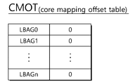
도 6은 논리 블록 어드레스 그룹 별 코어 맵핑 오프셋을 포함하는 코어 맵핑 오프셋 테이블을 나타낸 도면이다.
도 7은 본 발명의 실시 예에 따른 데이터 저장 장치의 동작 방법을 나타낸 순서도이다.
도 8은 본 발명의 실시 예에 따른 솔리드 스테이트 드라이브(SSD)를 포함하는 데이터 처리 시스템을 예시적으로 나타낸 도면이다.
도 9는 도 8의 컨트롤러의 구성을 예시적으로 나타낸 도면이다.
도 10은 본 발명의 실시 예에 따른 데이터 저장 장치를 포함하는 데이터 처리 시스템을 예시적으로 나타낸 도면이다.
도 11은 본 발명의 실시 예에 따른 데이터 저장 장치를 포함하는 데이터 처리 시스템을 예시적으로 나타낸 도면이다.
도 12는 본 발명의 실시 예에 따른 데이터 저장 장치를 포함하는 네트워크 시스템을 예시적으로 나타낸 도면이다.
도 13은 본 발명의 실시 예에 따른 데이터 저장 장치에 포함된 불휘발성 메모리 장치를 예시적으로 나타낸 블록도이다.
200: 컨트롤러 210: 제1 CPU
220: 제2 CPU 300: 휘발성 메모리
Claims (14)
- 불휘발성 메모리 장치; 및 상기 불휘발성 메모리 장치의 동작을 제어하는 컨트롤러를 포함하고,
상기 컨트롤러는, 제1 CPU 및 복수의 코어들을 포함하는 제2 CPU를 포함하고,
상기 제1 CPU는 기 설정된 주기 마다 상기 제2 CPU의 상기 복수의 코어들 각각에 대한 프로그램/소거(program/erase, P/E) 평균 카운트를 비교하고, 상기 복수의 코어들 중 상기 P/E 평균 카운트의 차이 값이 기 설정된 임계 값 이상인 제1 코어와 제2 코어가 존재하면, 호스트로부터 수신되는 논리 블록 어드레스들에 맵핑되는 코어를 변경하는 리-맵핑 동작을 수행하는 데이터 저장 장치. - 제1항에 있어서,
상기 데이터 저장 장치는, 휘발성 메모리를 더 포함하고,
상기 휘발성 메모리는,
상기 제2 CPU의 상기 복수의 코어들 각각에 대한 상기 P/E 평균 카운트로 구성된 프로그램/소거 카운트 테이블;
복수의 논리 블록 어드레스 그룹들 각각에 대한 코어 별 액세스 카운트로 구성된 코어 액세스 카운트 테이블; 및
상기 복수의 논리 블록 어드레스 그룹들 각각에 대한 코어 맵핑 오프셋으로 구성된 코어 맵핑 오프셋 테이블
을 포함하는 데이터 저장 장치. - 제2항에 있어서,
상기 제1 CPU는 상기 리-맵핑 동작을 수행하도록 구성된 리-맵핑 모듈을 포함하는 데이터 저장 장치. - 제3항에 있어서,
상기 제1 CPU는 상기 제2 CPU의 상기 복수의 코어들 중 상기 제1 코어와 상기 제2 코어가 존재하면, 상기 리-맵핑 모듈을 구동시켜 상기 리-맵핑 동작을 수행하는 데이터 저장 장치. - 제3항에 있어서,
상기 제1 코어의 P/E 평균 카운트가 상기 제2 코어의 P/E 평균 카운트보다 큰 경우,
상기 리-맵핑 모듈은 상기 코어 액세스 카운트 테이블을 참조하여 상기 복수의 논리 블록 어드레스 그룹들 중 상기 제1 코어의 액세스 카운트가 상기 제2 코어의 액세스 카운트보다 크고, 상기 제1 코어의 상기 액세스 카운트와 상기 제2 코어의 상기 액세스 카운트의 차이가 가장 큰 논리 블록 어드레스 그룹을 리-맵핑 대상 논리 블록 어드레스 그룹으로 선택하는 데이터 저장 장치. - 제5항에 있어서,
상기 리-맵핑 모듈은 상기 코어 맵핑 오프셋 테이블에서 상기 리-맵핑 대상 논리 블록 어드레스 그룹에 대응하는 상기 코어 맵핑 오프셋을 재설정하는 데이터 저장 장치. - 제6항에 있어서,
상기 리-맵핑 모듈은 리-맵핑 대상 논리 블록 어드레스 그룹에 대응하는 상기 코어 맵핑 오프셋을 상기 제1 코어부터 상기 제2 코어까지의 오프셋으로 변경하여 상기 코어 맵핑 오프셋을 재설정하는 데이터 저장 장치. - 제6항에 있어서,
상기 리-맵핑 모듈은 상기 코어 맵핑 오프셋을 재설정하기 전에, 상기 리-맵핑 대상 논리 블록 어드레스 그룹에 포함된 논리 블록 어드레스들 각각에 대응하는 데이터를 리-맵핑될 코어의 전용 저장 영역으로 이동시키기 위한 지시를 상기 제2 CPU의 상기 복수의 코어들 각각에 제공하는 데이터 저장 장치. - 제8항에 있어서,
상기 제2 CPU의 상기 복수의 코어들은 각각 상기 리-맵핑 모듈로부터 제공된 상기 지시에 따라 상기 리-맵핑 대상 논리 블록 어드레스 그룹에 포함된 상기 논리 블록 어드레스들 중 대응하는 적어도 하나의 논리 블록 어드레스에 대응하는 데이터를 상기 리-맵핑될 코어의 상기 전용 저장 영역으로 이동시키는 데이터 저장 장치. - 불휘발성 메모리 장치; 및 상기 불휘발성 메모리 장치의 동작을 제어하되, 제1 CPU 및 복수의 코어들을 포함하는 제2 CPU를 갖는 컨트롤러를 포함하는 데이터 저장 장치의 동작 방법으로서,
기 설정된 주기 마다 상기 제2 CPU의 상기 복수의 코어들 각각에 대한 프로그램/소거(program/erase, P/E) 평균 카운트를 비교하는 단계;
상기 제2 CPU의 상기 복수의 코어들 중 상기 P/E 평균 카운트의 차이 값이 기 설정된 임계 값 이상인 제1 코어와 제2 코어가 존재하는지 여부를 확인하는 단계; 및
상기 제1 코어와 상기 제2 코어가 존재하면, 호스트로부터 수신되는 논리 블록 어드레스들에 맵핑되는 코어를 변경하는 리-맵핑 동작을 수행하는 단계
를 포함하는 데이터 저장 장치의 동작 방법. - 제10항에 있어서,
상기 제1 코어의 P/E 평균 카운트가 상기 제2 코어의 P/E 평균 카운트보다 큰 경우,
상기 리-맵핑 동작을 수행하는 단계는,
복수의 논리 블록 어드레스 그룹들 중 상기 제1 코어의 액세스 카운트가 상기 제2 코어의 액세스 카운트보다 크고, 상기 제1 코어의 상기 액세스 카운트와 상기 제2 코어의 상기 액세스 카운트의 차이가 가장 큰 논리 블록 어드레스 그룹을 리-맵핑 대상 논리 블록 어드레스 그룹으로 선택하는 단계; 및
상기 리-맵핑 대상 논리 블록 어드레스 그룹에 대응하는 코어 맵핑 오프셋을 재설정하는 단계
를 포함하는 데이터 저장 장치의 동작 방법. - 제11항에 있어서,
상기 코어 맵핑 오프셋은 각 논리 블록 어드레스 그룹에 포함된 복수의 논리 블록 어드레스들 각각에 맵핑되는 코어를 결정하는 오프셋인 데이터 저장 장치의 동작 방법. - 제12항에 있어서,
상기 코어 맵핑 오프셋을 재설정하는 단계는,
상기 리-맵핑 대상 논리 블록 어드레스 그룹에 대응하는 상기 코어 맵핑 오프셋을 상기 제1 코어로부터 상기 제2 코어까지의 오프셋으로 변경하는 단계
를 포함하는 데이터 저장 장치의 동작 방법. - 제11항에 있어서,
상기 코어 맵핑 오프셋을 재설정하는 단계 이전에,
상기 리-맵핑 대상 논리 블록 어드레스 그룹에 포함된 논리 블록 어드레스들 각각에 대응하는 데이터를 리-맵핑될 코어의 전용 저장 영역으로 이동시키는 단계
를 더 포함하는 데이터 저장 장치의 동작 방법.
Priority Applications (3)
| Application Number | Priority Date | Filing Date | Title |
|---|---|---|---|
| KR1020190012769A KR102808981B1 (ko) | 2019-01-31 | 2019-01-31 | 데이터 저장 장치 및 그 동작 방법 |
| US16/660,651 US10949105B2 (en) | 2019-01-31 | 2019-10-22 | Data storage device and operating method of the data storage device |
| CN201911079270.5A CN111506516B (zh) | 2019-01-31 | 2019-11-07 | 数据存储装置及数据存储装置的操作方法 |
Applications Claiming Priority (1)
| Application Number | Priority Date | Filing Date | Title |
|---|---|---|---|
| KR1020190012769A KR102808981B1 (ko) | 2019-01-31 | 2019-01-31 | 데이터 저장 장치 및 그 동작 방법 |
Publications (2)
| Publication Number | Publication Date |
|---|---|
| KR20200095103A true KR20200095103A (ko) | 2020-08-10 |
| KR102808981B1 KR102808981B1 (ko) | 2025-05-16 |
Family
ID=71837434
Family Applications (1)
| Application Number | Title | Priority Date | Filing Date |
|---|---|---|---|
| KR1020190012769A Active KR102808981B1 (ko) | 2019-01-31 | 2019-01-31 | 데이터 저장 장치 및 그 동작 방법 |
Country Status (3)
| Country | Link |
|---|---|
| US (1) | US10949105B2 (ko) |
| KR (1) | KR102808981B1 (ko) |
| CN (1) | CN111506516B (ko) |
Cited By (13)
| Publication number | Priority date | Publication date | Assignee | Title |
|---|---|---|---|---|
| US11126379B2 (en) | 2019-11-25 | 2021-09-21 | SK Hynix Inc. | Memory system |
| US11194520B2 (en) | 2017-10-27 | 2021-12-07 | SK Hynix Inc. | Memory system and operating method thereof |
| US11360707B2 (en) | 2019-11-21 | 2022-06-14 | SK Hynix Inc. | Memory controller for replacing bad blocks with reserved blocks and operating method thereof |
| US11366763B2 (en) | 2019-02-27 | 2022-06-21 | SK Hynix Inc. | Controller including cache memory, memory system, and operating method thereof |
| US11436148B2 (en) | 2020-06-30 | 2022-09-06 | SK Hynix Inc. | Memory controller and method of operating the same |
| US11449235B2 (en) | 2020-06-25 | 2022-09-20 | SK Hynix Inc. | Storage device for processing merged transactions and method of operating the same |
| US11494313B2 (en) | 2020-04-13 | 2022-11-08 | SK Hynix Inc. | Cache memory including dedicated areas, storage device and method for storing data in the dedicated areas of the cache memory |
| US11573891B2 (en) | 2019-11-25 | 2023-02-07 | SK Hynix Inc. | Memory controller for scheduling commands based on response for receiving write command, storage device including the memory controller, and operating method of the memory controller and the storage device |
| US11599464B2 (en) | 2020-05-21 | 2023-03-07 | SK Hynix Inc. | Memory controller and method of operating the same |
| US11645197B2 (en) | 2020-05-18 | 2023-05-09 | SK Hynix Inc. | Memory controller and method of operating the same |
| US11934309B2 (en) | 2020-04-13 | 2024-03-19 | SK Hynix Inc. | Memory controller, storage device including the memory controller, and method of operating the memory controller and the storage device |
| US12118241B2 (en) | 2017-10-27 | 2024-10-15 | SK Hynix Inc. | Memory controller, memory system, and operating method thereof |
| US12164784B2 (en) | 2022-07-21 | 2024-12-10 | SK Hynix Inc. | Memory controller for performing wear-leveling and memory system including the same |
Families Citing this family (3)
| Publication number | Priority date | Publication date | Assignee | Title |
|---|---|---|---|---|
| KR102874986B1 (ko) * | 2020-10-06 | 2025-10-23 | 에스케이하이닉스 주식회사 | 저장 장치 및 그 동작 방법 |
| KR102934445B1 (ko) * | 2020-10-15 | 2026-03-06 | 에스케이하이닉스 주식회사 | 메모리 시스템 및 메모리 시스템의 동작방법 |
| US12190958B2 (en) | 2021-11-22 | 2025-01-07 | Samsung Electronics Co., Ltd. | Storage controller and storage device including the same |
Citations (4)
| Publication number | Priority date | Publication date | Assignee | Title |
|---|---|---|---|---|
| US20100088461A1 (en) * | 2008-10-02 | 2010-04-08 | Yang Wun Mo | Solid state storage system using global wear leveling and method of controlling the solid state storage system |
| US20120150527A1 (en) * | 2009-08-21 | 2012-06-14 | Tadhg Creedon | Storage peripheral device emulation |
| US20130265825A1 (en) * | 2012-04-10 | 2013-10-10 | Paul A. Lassa | System and method for micro-tiering in non-volatile memory |
| KR20150121560A (ko) * | 2014-04-21 | 2015-10-29 | 삼성전자주식회사 | 스토리지 장치, 스토리지 시스템 및 스토리지 시스템의 동작 방법 |
Family Cites Families (28)
| Publication number | Priority date | Publication date | Assignee | Title |
|---|---|---|---|---|
| US7653778B2 (en) * | 2006-05-08 | 2010-01-26 | Siliconsystems, Inc. | Systems and methods for measuring the useful life of solid-state storage devices |
| US9153337B2 (en) | 2006-12-11 | 2015-10-06 | Marvell World Trade Ltd. | Fatigue management system and method for hybrid nonvolatile solid state memory system |
| US20090150640A1 (en) | 2007-12-11 | 2009-06-11 | Royer Steven E | Balancing Computer Memory Among a Plurality of Logical Partitions On a Computing System |
| US7870363B2 (en) | 2007-12-28 | 2011-01-11 | Intel Corporation | Methods and arrangements to remap non-volatile storage |
| JP5221157B2 (ja) * | 2008-02-04 | 2013-06-26 | 株式会社日立製作所 | コンピュータシステム及び物理ディスク回収方法 |
| KR101516580B1 (ko) | 2009-04-22 | 2015-05-11 | 삼성전자주식회사 | 컨트롤러, 이를 포함하는 데이터 저장 장치 및 데이터 저장 시스템, 및 그 방법 |
| US8601202B1 (en) * | 2009-08-26 | 2013-12-03 | Micron Technology, Inc. | Full chip wear leveling in memory device |
| TWI423024B (zh) | 2009-11-23 | 2014-01-11 | Phison Electronics Corp | 用於快閃記憶體的資料儲存方法及其控制器與儲存系統 |
| US8869161B2 (en) | 2010-11-18 | 2014-10-21 | Fujitsu Limited | Characterization and assignment of workload requirements to resources based on predefined categories of resource utilization and resource availability |
| CN102511044B (zh) | 2011-09-06 | 2013-10-02 | 华为技术有限公司 | 一种数据删除方法及装置 |
| US8839073B2 (en) * | 2012-05-04 | 2014-09-16 | Lsi Corporation | Zero-one balance management in a solid-state disk controller |
| US9274839B2 (en) | 2012-09-27 | 2016-03-01 | Intel Corporation | Techniques for dynamic physical memory partitioning |
| WO2014105058A1 (en) | 2012-12-28 | 2014-07-03 | Intel Corporation | Optimal logical processor count and type selection for a given workload on platform thermals and power budgeting constraints |
| US9384059B2 (en) | 2013-05-31 | 2016-07-05 | Hitachi, Ltd. | Comparing resource costs between allocation plans in a load balance apparatus |
| KR102128472B1 (ko) | 2014-02-17 | 2020-06-30 | 삼성전자주식회사 | 인-스토리지 컴퓨팅 동작들을 수행할 수 있는 스토리지 장치, 이의 동작 방법, 및 이를 포함하는 시스템 |
| US10261697B2 (en) | 2015-06-08 | 2019-04-16 | Samsung Electronics Co., Ltd. | Storage device and operating method of storage device |
| TWI601059B (zh) * | 2015-11-19 | 2017-10-01 | 慧榮科技股份有限公司 | 資料儲存裝置與資料儲存方法 |
| US10101939B2 (en) * | 2016-03-09 | 2018-10-16 | Toshiba Memory Corporation | Storage system having a host that manages physical data locations of a storage device |
| KR102509986B1 (ko) | 2016-03-28 | 2023-03-14 | 삼성전자주식회사 | 다중 코어 프로세서 및 다중 코어 프로세서를 제어하는 방법 |
| KR102610537B1 (ko) | 2016-11-10 | 2023-12-06 | 삼성전자주식회사 | 솔리드 스테이트 드라이브 장치 및 이를 포함하는 저장 시스템 |
| US10338983B2 (en) * | 2016-12-30 | 2019-07-02 | EMC IP Holding Company LLC | Method and system for online program/erase count estimation |
| KR102395538B1 (ko) * | 2017-04-28 | 2022-05-10 | 에스케이하이닉스 주식회사 | 데이터 저장 장치 및 그것의 동작 방법 |
| CN107391391B (zh) | 2017-07-19 | 2019-05-14 | 深圳大普微电子科技有限公司 | 在固态硬盘的ftl实现数据拷贝的方法、系统及固态硬盘 |
| US20190227618A1 (en) | 2018-01-23 | 2019-07-25 | Goke Us Research Laboratory | Power Management for a Data Storage Apparatus |
| JP6967986B2 (ja) | 2018-01-29 | 2021-11-17 | キオクシア株式会社 | メモリシステム |
| US10956318B2 (en) | 2018-06-19 | 2021-03-23 | Macronix International Co., Ltd. | Overlapping ranges of pages in memory systems |
| US20200233588A1 (en) | 2019-01-23 | 2020-07-23 | Alibaba Group Holding Limited | Efficient lightweight storage nodes |
| KR102852744B1 (ko) | 2019-04-03 | 2025-09-01 | 에스케이하이닉스 주식회사 | 컨트롤러, 이를 포함하는 메모리 시스템 및 메모리 시스템의 동작 방법 |
-
2019
- 2019-01-31 KR KR1020190012769A patent/KR102808981B1/ko active Active
- 2019-10-22 US US16/660,651 patent/US10949105B2/en active Active
- 2019-11-07 CN CN201911079270.5A patent/CN111506516B/zh active Active
Patent Citations (4)
| Publication number | Priority date | Publication date | Assignee | Title |
|---|---|---|---|---|
| US20100088461A1 (en) * | 2008-10-02 | 2010-04-08 | Yang Wun Mo | Solid state storage system using global wear leveling and method of controlling the solid state storage system |
| US20120150527A1 (en) * | 2009-08-21 | 2012-06-14 | Tadhg Creedon | Storage peripheral device emulation |
| US20130265825A1 (en) * | 2012-04-10 | 2013-10-10 | Paul A. Lassa | System and method for micro-tiering in non-volatile memory |
| KR20150121560A (ko) * | 2014-04-21 | 2015-10-29 | 삼성전자주식회사 | 스토리지 장치, 스토리지 시스템 및 스토리지 시스템의 동작 방법 |
Cited By (15)
| Publication number | Priority date | Publication date | Assignee | Title |
|---|---|---|---|---|
| US11194520B2 (en) | 2017-10-27 | 2021-12-07 | SK Hynix Inc. | Memory system and operating method thereof |
| US12118241B2 (en) | 2017-10-27 | 2024-10-15 | SK Hynix Inc. | Memory controller, memory system, and operating method thereof |
| US11366763B2 (en) | 2019-02-27 | 2022-06-21 | SK Hynix Inc. | Controller including cache memory, memory system, and operating method thereof |
| US11360707B2 (en) | 2019-11-21 | 2022-06-14 | SK Hynix Inc. | Memory controller for replacing bad blocks with reserved blocks and operating method thereof |
| US11573891B2 (en) | 2019-11-25 | 2023-02-07 | SK Hynix Inc. | Memory controller for scheduling commands based on response for receiving write command, storage device including the memory controller, and operating method of the memory controller and the storage device |
| US12222855B2 (en) | 2019-11-25 | 2025-02-11 | SK Hynix Inc. | Memory controller for scheduling commands based on response for receiving write command, storage device including the memory controller, and operating method of the memory controller and the storage device |
| US11126379B2 (en) | 2019-11-25 | 2021-09-21 | SK Hynix Inc. | Memory system |
| US11494313B2 (en) | 2020-04-13 | 2022-11-08 | SK Hynix Inc. | Cache memory including dedicated areas, storage device and method for storing data in the dedicated areas of the cache memory |
| US11934309B2 (en) | 2020-04-13 | 2024-03-19 | SK Hynix Inc. | Memory controller, storage device including the memory controller, and method of operating the memory controller and the storage device |
| US12332784B2 (en) | 2020-04-13 | 2025-06-17 | SK Hynix Inc. | Memory controller, storage device including the memory controller, and method of operating the memory controller and the storage device |
| US11645197B2 (en) | 2020-05-18 | 2023-05-09 | SK Hynix Inc. | Memory controller and method of operating the same |
| US11599464B2 (en) | 2020-05-21 | 2023-03-07 | SK Hynix Inc. | Memory controller and method of operating the same |
| US11449235B2 (en) | 2020-06-25 | 2022-09-20 | SK Hynix Inc. | Storage device for processing merged transactions and method of operating the same |
| US11436148B2 (en) | 2020-06-30 | 2022-09-06 | SK Hynix Inc. | Memory controller and method of operating the same |
| US12164784B2 (en) | 2022-07-21 | 2024-12-10 | SK Hynix Inc. | Memory controller for performing wear-leveling and memory system including the same |
Also Published As
| Publication number | Publication date |
|---|---|
| US20200249854A1 (en) | 2020-08-06 |
| CN111506516B (zh) | 2023-03-07 |
| US10949105B2 (en) | 2021-03-16 |
| CN111506516A (zh) | 2020-08-07 |
| KR102808981B1 (ko) | 2025-05-16 |
Similar Documents
| Publication | Publication Date | Title |
|---|---|---|
| KR102808981B1 (ko) | 데이터 저장 장치 및 그 동작 방법 | |
| US11216362B2 (en) | Data storage device and operating method thereof | |
| KR102691851B1 (ko) | 불휘발성 메모리 장치, 이를 포함하는 데이터 저장 장치 및 그 동작 방법 | |
| US10877887B2 (en) | Data storage device and operating method thereof | |
| US20200218653A1 (en) | Controller, data storage device, and operating method thereof | |
| US11068206B2 (en) | Data storage device for processing a sequential unmap entry by using trim instruction data and operating method thereof | |
| US11249897B2 (en) | Data storage device and operating method thereof | |
| KR102839226B1 (ko) | 컨트롤러 및 그것의 동작 방법과 메모리 시스템 | |
| KR102419036B1 (ko) | 데이터 저장 장치 및 그것의 동작 방법 | |
| US20200310956A1 (en) | Data storage device and operating method thereof | |
| KR102707997B1 (ko) | 컨트롤러, 메모리 시스템 및 그것의 동작 방법 | |
| KR20210156010A (ko) | 저장 장치 및 그 동작 방법 | |
| KR20210144249A (ko) | 저장 장치 및 이의 동작 방법 | |
| KR102469174B1 (ko) | 데이터 저장 장치 및 그것의 동작 방법 | |
| KR102695482B1 (ko) | 데이터 저장 장치 및 그것의 동작 방법 | |
| KR20190061942A (ko) | 데이터 저장 장치 및 그것의 동작 방법 | |
| US11281590B2 (en) | Controller, operating method thereof and storage device including the same | |
| KR102742128B1 (ko) | 저장 장치 및 그 동작 방법 | |
| US20210397558A1 (en) | Storage device and operating method thereof | |
| KR102836067B1 (ko) | 컨트롤러, 메모리 시스템 및 그것의 동작 방법 | |
| US11157401B2 (en) | Data storage device and operating method thereof performing a block scan operation for checking for valid page counts | |
| KR102835936B1 (ko) | 데이터 저장 장치, 이를 포함하는 전자 장치 및 데이터 저장 장치의 동작 방법 | |
| US11314461B2 (en) | Data storage device and operating method of checking success of garbage collection operation | |
| KR20200042780A (ko) | 데이터 저장 장치 및 그것의 동작 방법 | |
| KR20190099570A (ko) | 데이터 저장 장치 및 그것의 동작 방법 |
Legal Events
| Date | Code | Title | Description |
|---|---|---|---|
| PA0109 | Patent application |
Patent event code: PA01091R01D Comment text: Patent Application Patent event date: 20190131 |
|
| PG1501 | Laying open of application | ||
| A201 | Request for examination | ||
| PA0201 | Request for examination |
Patent event code: PA02012R01D Patent event date: 20220111 Comment text: Request for Examination of Application Patent event code: PA02011R01I Patent event date: 20190131 Comment text: Patent Application |
|
| E902 | Notification of reason for refusal | ||
| PE0902 | Notice of grounds for rejection |
Comment text: Notification of reason for refusal Patent event date: 20240821 Patent event code: PE09021S01D |
|
| E701 | Decision to grant or registration of patent right | ||
| PE0701 | Decision of registration |
Patent event code: PE07011S01D Comment text: Decision to Grant Registration Patent event date: 20250225 |
|
| GRNT | Written decision to grant | ||
| PR0701 | Registration of establishment |
Comment text: Registration of Establishment Patent event date: 20250513 Patent event code: PR07011E01D |
|
| PR1002 | Payment of registration fee |
Payment date: 20250514 End annual number: 3 Start annual number: 1 |
|
| PG1601 | Publication of registration |