KR20200096228A - 정류 회로 및 이를 포함하는 장치 - Google Patents
정류 회로 및 이를 포함하는 장치 Download PDFInfo
- Publication number
- KR20200096228A KR20200096228A KR1020207015819A KR20207015819A KR20200096228A KR 20200096228 A KR20200096228 A KR 20200096228A KR 1020207015819 A KR1020207015819 A KR 1020207015819A KR 20207015819 A KR20207015819 A KR 20207015819A KR 20200096228 A KR20200096228 A KR 20200096228A
- Authority
- KR
- South Korea
- Prior art keywords
- circuit
- transistors
- input
- voltage
- transistor
- Prior art date
- Legal status (The legal status is an assumption and is not a legal conclusion. Google has not performed a legal analysis and makes no representation as to the accuracy of the status listed.)
- Granted
Links
Images


Classifications
-
- H—ELECTRICITY
- H02—GENERATION; CONVERSION OR DISTRIBUTION OF ELECTRIC POWER
- H02M—APPARATUS FOR CONVERSION BETWEEN AC AND AC, BETWEEN AC AND DC, OR BETWEEN DC AND DC, AND FOR USE WITH MAINS OR SIMILAR POWER SUPPLY SYSTEMS; CONVERSION OF DC OR AC INPUT POWER INTO SURGE OUTPUT POWER; CONTROL OR REGULATION THEREOF
- H02M7/00—Conversion of AC power input into DC power output; Conversion of DC power input into AC power output
- H02M7/02—Conversion of AC power input into DC power output without possibility of reversal
- H02M7/04—Conversion of AC power input into DC power output without possibility of reversal by static converters
- H02M7/12—Conversion of AC power input into DC power output without possibility of reversal by static converters using discharge tubes with control electrode or semiconductor devices with control electrode
- H02M7/21—Conversion of AC power input into DC power output without possibility of reversal by static converters using discharge tubes with control electrode or semiconductor devices with control electrode using devices of a triode or transistor type requiring continuous application of a control signal
- H02M7/217—Conversion of AC power input into DC power output without possibility of reversal by static converters using discharge tubes with control electrode or semiconductor devices with control electrode using devices of a triode or transistor type requiring continuous application of a control signal using semiconductor devices only
- H02M7/2176—Conversion of AC power input into DC power output without possibility of reversal by static converters using discharge tubes with control electrode or semiconductor devices with control electrode using devices of a triode or transistor type requiring continuous application of a control signal using semiconductor devices only comprising a passive stage to generate a rectified sinusoidal voltage and a controlled switching element in series between such stage and the output
-
- H—ELECTRICITY
- H02—GENERATION; CONVERSION OR DISTRIBUTION OF ELECTRIC POWER
- H02M—APPARATUS FOR CONVERSION BETWEEN AC AND AC, BETWEEN AC AND DC, OR BETWEEN DC AND DC, AND FOR USE WITH MAINS OR SIMILAR POWER SUPPLY SYSTEMS; CONVERSION OF DC OR AC INPUT POWER INTO SURGE OUTPUT POWER; CONTROL OR REGULATION THEREOF
- H02M7/00—Conversion of AC power input into DC power output; Conversion of DC power input into AC power output
- H02M7/02—Conversion of AC power input into DC power output without possibility of reversal
- H02M7/04—Conversion of AC power input into DC power output without possibility of reversal by static converters
- H02M7/12—Conversion of AC power input into DC power output without possibility of reversal by static converters using discharge tubes with control electrode or semiconductor devices with control electrode
- H02M7/21—Conversion of AC power input into DC power output without possibility of reversal by static converters using discharge tubes with control electrode or semiconductor devices with control electrode using devices of a triode or transistor type requiring continuous application of a control signal
- H02M7/217—Conversion of AC power input into DC power output without possibility of reversal by static converters using discharge tubes with control electrode or semiconductor devices with control electrode using devices of a triode or transistor type requiring continuous application of a control signal using semiconductor devices only
- H02M7/219—Conversion of AC power input into DC power output without possibility of reversal by static converters using discharge tubes with control electrode or semiconductor devices with control electrode using devices of a triode or transistor type requiring continuous application of a control signal using semiconductor devices only in a bridge configuration
-
- H—ELECTRICITY
- H04—ELECTRIC COMMUNICATION TECHNIQUE
- H04B—TRANSMISSION
- H04B1/00—Details of transmission systems, not covered by a single one of groups H04B3/00 - H04B13/00; Details of transmission systems not characterised by the medium used for transmission
- H04B1/06—Receivers
- H04B1/16—Circuits
-
- H—ELECTRICITY
- H04—ELECTRIC COMMUNICATION TECHNIQUE
- H04B—TRANSMISSION
- H04B5/00—Near-field transmission systems, e.g. inductive or capacitive transmission systems
- H04B5/70—Near-field transmission systems, e.g. inductive or capacitive transmission systems specially adapted for specific purposes
- H04B5/79—Near-field transmission systems, e.g. inductive or capacitive transmission systems specially adapted for specific purposes for data transfer in combination with power transfer
-
- Y—GENERAL TAGGING OF NEW TECHNOLOGICAL DEVELOPMENTS; GENERAL TAGGING OF CROSS-SECTIONAL TECHNOLOGIES SPANNING OVER SEVERAL SECTIONS OF THE IPC; TECHNICAL SUBJECTS COVERED BY FORMER USPC CROSS-REFERENCE ART COLLECTIONS [XRACs] AND DIGESTS
- Y02—TECHNOLOGIES OR APPLICATIONS FOR MITIGATION OR ADAPTATION AGAINST CLIMATE CHANGE
- Y02B—CLIMATE CHANGE MITIGATION TECHNOLOGIES RELATED TO BUILDINGS, e.g. HOUSING, HOUSE APPLIANCES OR RELATED END-USER APPLICATIONS
- Y02B70/00—Technologies for an efficient end-user side electric power management and consumption
- Y02B70/10—Technologies improving the efficiency by using switched-mode power supplies [SMPS], i.e. efficient power electronics conversion e.g. power factor correction or reduction of losses in power supplies or efficient standby modes
Landscapes
- Engineering & Computer Science (AREA)
- Power Engineering (AREA)
- Computer Networks & Wireless Communication (AREA)
- Signal Processing (AREA)
- Rectifiers (AREA)
- Dc-Dc Converters (AREA)
- Input Circuits Of Receivers And Coupling Of Receivers And Audio Equipment (AREA)
- Amplifiers (AREA)
- Transmitters (AREA)
Abstract
Description
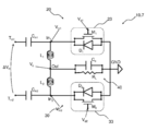
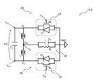
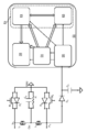
도 1 내지 도 9는 본 발명의 실시예에 따른 각각의 정류 회로의 개념 회로도이다.
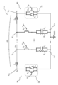
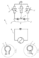
도 10a 및 도 10b는 본 발명의 각 실시예에 따른 제어 모듈이 개략적으로 도시된 정류 회로의 개념 회로도이다.
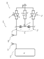
도 11은 본 발명의 일 실시예에 따른 전원 장치의 개념 회로도이다.
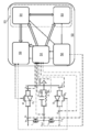
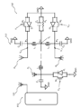
도 12는 본 발명의 일 실시예에 따른 유도성 에너지 전송 시스템의 개념 회로도이다.
도 13은 본 발명의 일 실시예에 따른 정전용량성 에너지 전송 시스템의 개념 회로도이다.
도 14a는 본 발명의 일 실시예에 따른 무선 주파수 에너지 전송 시스템의 개념 회로도이다.
도 14b는 본 발명의 일 실시예에 따른 다중 안테나 무선 주파수 에너지 전송 시스템의 개념 회로도이다.
Claims (38)
- 출력 노드(Out)와 기준 노드(GND) 사이에 병렬로 제 1 회로 브랜치(20) 및 제 2 회로 브랜치(30)를 포함하는 정류 회로(10, 10.1-10.9)로서,
각 회로 브랜치(20, 30)는 전류 제어 소자(23, 33)와 직렬로 유도 소자(L1, L2) 및 상기 전류 제어 소자(23, 33)와 상기 유도 소자(L1, L2) 사이에 배열된 입력 노드(In1, In2)를 각각 포함하고,
정류 회로의 동작 동안 입력 노드(In1, In2) 사이에 시간에 따라 변하는 입력 전압(ΔVin)이 인가되는 정류 회로. - 제 1 항에 있어서,
각각의 전류 제어 소자(23, 33)는 다이오드(D1, D2)를 포함하고, 상기 다이오드(D1, D2)의 애노드는 기준 노드(GND)에 연결되며, 상기 다이오드(D1, D2)의 캐소드는 각각의 입력 노드(In1, In2)에 연결되는 정류 회로. - 제 1 항에 있어서,
각각의 전류 제어 소자(23, 33)는 다이오드(D1, D2)를 포함하고, 상기 다이오드(D1, D2)의 애노드는 각각의 입력 노드(In1, In2)에 연결되며, 상기 다이오드(D1, D2)의 캐소드는 출력 노드(Out)에 연결되는 정류 회로. - 제 1 항 내지 제 3 항 중 어느 한 항에 있어서,
각 전류 제어 소자(23, 33)는 트랜지스터(M1, M2)를 포함하고, 상기 트랜지스터(M1, M2)는 기준 노드(GND)에 연결된 제 1 전도 단자 및 각각의 입력 노드(In1, In2)에 연결된 제 2 전도 단자를 포함하는 정류 회로. - 제 2 항 내지 제 4 항 중 어느 한 항에 있어서,
각각의 전류 제어 소자(23, 33)는 트랜지스터(M1, M2) 및 다이오드(D1, D2)를 포함하고, 상기 트랜지스터(M1, M2)는 다이오드(D1, D2)와 병렬인 정류 회로. - 제 4 항 또는 제 5 항에 있어서,
각각의 트랜지스터(M1, M2)는 바람직하게는 n형 또는 대안으로 p형의 실리콘 전계효과 트랜지스터, 바람직하게는 높은 전자 이동성(HEMT)을 갖는 전계효과 트랜지스터, 바람직하게는 GaN, GaAs, AlGaN, AlGaAs, InGaN, InGaAs, SiC, 바이폴라 트랜지스터, 절연 게이트 바이폴라 트랜지스터 또는 IGBT로부터 선택되는 정류 회로. - 제 6 항에 있어서,
각각의 트랜지스터(M1, M2)는 전계효과 트랜지스터이고, 전계효과 트랜지스터의 소스 단자는 기준 노드(GND)에 연결되며, 전계효과 트랜지스터의 드레인 단자는 각각의 입력 노드(In1, In2)에 연결되는 정류 회로. - 제 4 항 내지 제 6 항 중 어느 한 항에 있어서,
각각의 전류 제어 소자(23, 33)는 추가 트랜지스터(M3, M4)를 포함하고, 상기 추가 트랜지스터(M3, M4)는 각각의 트랜지스터(M1, M3)에 카운터 시리즈로 연결되는 정류 회로. - 제 1 항 내지 제 8 항 중 어느 한 항에 있어서,
정전용량성 소자(Co)와 부하 소자(R1)는 정류 회로(10, 10.1-10.9)의 출력 노드(Out)와 기준 노드(GND) 사이에 병렬로 연결되는 정류 회로. - 제 9 항에 있어서,
정전용량성 소자(Co)에 직렬로 연결되고 부하 소자(R1)에 서로 병렬로 연결된 트랜지스터(M5, M6.1-M6.n)를 포함하는 추가 전류 제어 소자(43)를 제공하고,
트랜지스터(M5, M6.1-M6.n)들은 직렬로 정전용량성 소자(Co)와 부하 소자(R1) 간에는 병렬로 출력 노드(Out)와 기준 노드(GND) 사이에 연결되는 정류 회로. - 제 1 항 내지 제 10 항 중 어느 한 항에 있어서,
회로 브랜치(20, 30)의 입력 노드(In1, In2)에 연결된 정전용량성 소자(Cp)를 더 포함하는 정류 회로. - 제 9 항에 있어서,
정전용량성 소자(Cp)는 유도 소자(L1, L2)와 조합하여 미리 결정된 공진 주파수를 정의하도록 크기가 정해지는 정류 회로. - 제 1 항 내지 제 12 항 중 어느 한 항에 있어서,
입력 전압(ΔVin)을 수신하기 위한 한 쌍의 입력 단자(Tin1, Tin2)를 더 포함하고, 각 회로 브랜치(20, 30)는 입력 노드(In1, In2) 및 각각의 입력 단자(Tin1, Tin2)에 연결된 디커플링 소자(Cin1, Cin2)를 더 포함하는 정류 회로. - 제 11 항에 있어서,
각각의 디커플링 소자(Cin1, Cin2)는 각각의 정전용량성 소자(Cin1, Cin2)를 포함하고, 상기 정전용량성 소자(Cin1, Cin2)는 유도 소자(L1, L2)와 조합하여 미리 결정된 공진 주파수를 정의하도록 크기가 정해지는 정류 회로. - 제 4 항 또는 제 4 항에 따른 청구항 중 어느 한 항에 있어서,
제어 모듈(50)을 더 포함하고, 각 트랜지스터(M1, M2)는 각각의 파일럿 신호(Vd1, Vd2)를 수신하기 위해 제어 모듈(50)에 연결된 제어 단자를 더 포함하고,
상기 제어 모듈(50)은:
회로의 노드 및 정류 회로의 소자로부터 적어도 하나에서 전압 및 전류로부터 적어도 하나의 값을 측정하기에 적합한 측정 유닛(51); 및
각각의 트랜지스터(M1, M2)에 대해 측정된 적어도 하나의 값에 기초하여 파일럿 신호(Vd1, Vd2)를 생성하고 각각의 트랜지스터(M1, M2)의 제어 단자에 상기 파일럿 신호(Vd1, Vd2)를 공급하기에 적합한 파일럿 유닛(53)을 포함하는 정류 회로. - 제 15 항에 있어서,
측정 유닛(51)은:
제 1 회로 브랜치(20)의 입력 노드(In1)에서의 전압;
제 1 회로 브랜치(20)의 전류 제어 소자(23)를 통해 흐르는 전류;
제 1 회로 브랜치(20)의 전류 제어 소자(23)에 의해 흡수된 전력;
제 2 회로 브랜치(30)의 입력 노드(In2)에서의 전압;
제 2 회로 브랜치(30)의 전류 제어 소자(33)를 통해 흐르는 전류;
제 2 회로 브랜치(30)의 전류 제어 소자(33)에 의해 흡수된 전력; 및
정류 회로(10, 10.1-10.9)의 출력 노드(Out)에서의 전압 중 적어도 하나를 측정하도록 구성되는 정류 회로. - 제 16 항 또는 제 9 항에 있어서,
측정 유닛(51)은:
부하 소자(R1)를 통해 흐르는 전류;
정전용량성 소자(Co)를 통해 흐르는 전류; 및
부하 소자(R1)에 의해 흡수된 전력 중 적어도 하나를 측정하도록 구성되는 정류 회로. - 제 15 항 내지 제 17 항 중 어느 한 항에 있어서,
제어 모듈(50)은 출력 노드(out), 파일럿 유닛(53) 및 측정 유닛(51)에 연결된 전원 유닛(56)을 더 포함하고, 상기 전원 유닛(56)은 출력 노드(Out)로부터 에너지를 흡수하고 작동을 위해 파일럿 유닛(53) 및 측정 유닛(51)에 에너지를 공급하는 정류 회로. - 제 15 항 내지 제 17 항 중 어느 한 항에 있어서,
제어 모듈(50)은 입력 노드(In1, In2) 및 전원 유닛(56)에 연결된 다이오드(D3)를 통해 입력 노드(In1, In2)에 연결된 전원 유닛(56) 및 상기 전원 유닛(56) 및 기준 노드(GND)에 연결된 콘덴서(C3)를 더 포함하고, 상기 전원 유닛(56)은 또한 파일럿 유닛(53) 및 측정 유닛(51)에 연결되며, 상기 전원 유닛(56)은 입력 노드(In1, In2)로부터 에너지를 흡수하고 작동을 위해 파일럿 유닛(53) 및 측정 유닛(51)으로 공급하는 정류 회로. - 제 18 항 또는 제 19 항에 있어서,
전원 유닛(56)은 로우 드롭아웃 레귤레이터 또는 LDO(Low-Dropout) 레귤레이터를 포함하는 정류 회로. - 제 15 항 내지 제 20 항 중 어느 한 항에 있어서,
파일럿 유닛(53)은:
각각의 트랜지스터(M1, M2)에 공급된 파일럿 신호(Vd1, Vd2)의 스위칭 및 적어도 하나의 측정값에 기초하여 정류 회로의 대응하는 응답과 관련된 적어도 하나의 지연을 추정하기에 적합한 지연 추정 블록(63); 및
식별된 지연에 기초하여 각각의 트랜지스터(M1, M2)에 대한 파일럿 신호(Vd1, Vd2)를 생성하기에 적합한 논리 블록(61)을 포함하는 정류 회로. - 제 21 항에 있어서,
파일럿 블록(61)은 적어도 하나의 측정값 및 식별된 지연에 기초하여 각각의 트랜지스터(M1, M2)에 대한 파일럿 신호(Vd1, Vd2)를 생성하기에 적합한 정류 회로. - 제 21 항 또는 제 22 항에 있어서,
지연 추정 블록(63)은 각각의 트랜지스터(M1, M2)를 활성화시키기에 적합한 파일럿 신호(Vd1, Vd2)의 제 1 스위칭 및 이에 대한 정류 회로의 대응하는 응답과 관련된 활성화 지연을 추정하도록 구성되는 정류 회로. - 제 23 항에 있어서,
지연 추정 블록(63)은 각각의 트랜지스터(M1, M2)를 스위치 오프하기에 적합한 파일럿 신호(Vd1, Vd2)의 제 2 스위칭 및 이에 대한 정류 회로의 대응하는 응답과 관련된 스위칭 오프 지연을 추정하도록 구성되는 정류 회로. - 제 21 항 내지 제 25 항 중 어느 한 항에 있어서,
논리 블록(61)은 적어도 하나의 미리 결정된 제 1 파일럿 테스트 신호 및 제 2 파일럿 테스트 신호를 생성하고 이를 제 1 회로 브랜치(20)의 트랜지스터(M1) 및 제 2 회로 브랜치(30)의 트랜지스터(M2)에 각각 공급하도록 구성되고, 지연 추정 블록(63)은 파일럿 테스트 신호에 대한 정류 회로의 응답에서 지연을 추정하도록 구성되는 정류 회로. - 제 25 항에 있어서,
논리 블록(61)은 제어 모듈(50)의 활성화시에 파일럿 테스트 신호를 생성하도록 구성되는 정류 회로. - 제 21 항 내지 제 26 항 중 어느 한 항에 있어서,
논리 블록(61)은 지연 추정 블록(63)에 의해 식별된 지연을 보상하기 위해 파일럿 신호를 더 일찍 생성하도록 구성되는 정류 회로. - 제 27 항에 있어서,
논리 블록(61)은 각각의 전류 제어 소자(23, 33)에 의해 흡수된 전력을 최소화하도록 지연을 보상하도록 구성되는 정류 회로. - 제 28 항에 있어서,
논리 블록(61)은 부하 소자(R1)에 의해 흡수된 전력을 최대화하도록 지연을 보상하게 구성되는 정류 회로. - 제 15 항 내지 제 29 항 중 어느 한 항에 있어서,
입력 전압(ΔVin)은 주기적으로 교번하는 반대 반파를 포함하여 시간에 따라 변하는 전압이고, 각 회로 브랜치(20, 30)는 상기 입력 전압(ΔVin)의 각각의 반파를 연속 출력 전압(Vout)으로 변환하는데 적합하며, 파일럿 유닛(53)은 입력 전압(ΔVin)의 각각의 반파의 변환을 선택적으로 억제하기 위해 각각의 트랜지스터(M1, M2)에 대해 파일럿 신호(Vd1, Vd2)를 생성하도록 구성되는 정류 회로. - 제 1 항 내지 제 30 항 중 어느 한 항에 있어서,
각각의 유도 소자(L1, L2)는 자기적으로 절연된 인덕터인 정류 회로. - 제 1 항 내지 제 31 항 중 어느 한 항에 있어서,
각각의 유도 소자(L1, L2)는 변압기의 권선을 포함하지 않는 정류 회로. - 제 1 항 내지 제 32 항 중 어느 한 항에 따른 정류 회로(10, 10.1-10.9)를 포함하는 전원 장치(70).
- 제 1 항 내지 제 30 항 중 어느 한 항에 따른 정류 회로(10, 10.1-10.9)를 포함하는 유도 수신기 회로(80)로서,
각각의 유도 소자(L1, L2)는 각각의 수신 코일(L1, L2)을 포함하는 유도 수신기 회로. - 제 32 항에 있어서,
코일(L1, L2)은 서로 중첩되는 유도 수신기 회로. - 제 1 항 내지 제 30 항 중 어느 한 항에 따른 정류 회로(10, 10.1-10.9)를 포함하는 정전용량성 수신기 회로(90)로서,
각각의 입력 노드(In1, In2)가 각각의 전도성 수신 플레이트(103.1, 103.2)에 연결되는 수신기 회로. - 제 1 항 내지 제 30 항 중 어느 한 항에 따른 정류 회로(10, 10.1-10.9)를 포함하는 무선 주파수 수신기 회로(110)로서,
입력 노드(In1, In2) 중 적어도 하나가 안테나(123)에 연결되는 무선 주파수 수신기 회로. - 제 35 항에 있어서,
각각의 안테나에 연결된 적어도 하나의 추가 회로 브랜치를 더 포함하고, 각각의 브랜치는 각각의 주파수에서 공진하는 각각의 인덕터 및 콘덴서 쌍을 포함하는 무선 주파수 수신기 회로.
Applications Claiming Priority (3)
| Application Number | Priority Date | Filing Date | Title |
|---|---|---|---|
| IT201700139734 | 2017-12-04 | ||
| IT102017000139734 | 2017-12-04 | ||
| PCT/IB2018/058734 WO2019111076A1 (en) | 2017-12-04 | 2018-11-07 | Rectifying circuit and devices comprising the same |
Publications (2)
| Publication Number | Publication Date |
|---|---|
| KR20200096228A true KR20200096228A (ko) | 2020-08-11 |
| KR102432265B1 KR102432265B1 (ko) | 2022-08-12 |
Family
ID=61527471
Family Applications (1)
| Application Number | Title | Priority Date | Filing Date |
|---|---|---|---|
| KR1020207015819A Active KR102432265B1 (ko) | 2017-12-04 | 2018-11-07 | 정류 회로 및 이를 포함하는 장치 |
Country Status (7)
| Country | Link |
|---|---|
| US (1) | US11050356B2 (ko) |
| EP (1) | EP3721539B1 (ko) |
| JP (1) | JP7082203B2 (ko) |
| KR (1) | KR102432265B1 (ko) |
| CN (1) | CN111542994B (ko) |
| TW (1) | TWI785146B (ko) |
| WO (1) | WO2019111076A1 (ko) |
Families Citing this family (11)
| Publication number | Priority date | Publication date | Assignee | Title |
|---|---|---|---|---|
| EP3648362B1 (fr) * | 2018-11-02 | 2021-03-03 | Stmicroelectronics Sa | Procédé de limitation du niveau de tension issue d'un champ magnétique reçu par un transpondeur et transpondeur correspondant |
| CN110730540A (zh) * | 2019-10-17 | 2020-01-24 | 横店集团得邦照明股份有限公司 | 一种采用电感串联方式的led电路及其实现方法 |
| TWI747347B (zh) * | 2020-06-30 | 2021-11-21 | 至美科技股份有限公司 | 具有半電流倍增輸出之相移全橋轉換器及其控制方法 |
| US11545943B2 (en) * | 2020-12-04 | 2023-01-03 | Mks Instruments, Inc. | Switched capacitor modulator |
| JP7529946B2 (ja) * | 2021-02-17 | 2024-08-07 | ミネベアパワーデバイス株式会社 | 整流回路、整流回路の制御方法 |
| TWI806184B (zh) * | 2021-10-08 | 2023-06-21 | 宏碁股份有限公司 | 供電裝置 |
| JP2025501604A (ja) * | 2021-12-22 | 2025-01-22 | ソレース・パワー・インコーポレイテッド | ワイヤレス電力レシーバで使用するための差動整流器および電力信号を整流する方法 |
| CN114665701B (zh) * | 2022-03-30 | 2025-07-11 | 西北工业大学 | 获取桥式变换器的吸收电路参数的方法、装置和电路 |
| TWI806548B (zh) * | 2022-04-13 | 2023-06-21 | 宏碁股份有限公司 | 升壓轉換器 |
| TWI848435B (zh) * | 2022-11-11 | 2024-07-11 | 康舒科技股份有限公司 | 空乏式氮化鎵電晶體同步整流器及具有同步整流器的電源轉換器 |
| CN116131623B (zh) * | 2023-02-20 | 2025-04-15 | 重庆大学 | 一种低成本的单输入可调节多输出wpt系统及其控制方法 |
Citations (5)
| Publication number | Priority date | Publication date | Assignee | Title |
|---|---|---|---|---|
| US20110017032A1 (en) * | 2009-07-21 | 2011-01-27 | World Color Press Inc. | Variable trimming equipment, systems, and methods |
| US20120022439A1 (en) * | 2007-10-24 | 2012-01-26 | Minimus Spine, Inc. | Syringe, system and method for delivering oxygen-ozone |
| US20140008490A1 (en) * | 2008-06-20 | 2014-01-09 | Brigham Young University | Aerial recovery of small and micro air vehicles |
| US20150033353A1 (en) * | 2003-07-01 | 2015-01-29 | Securityprofiling, Llc | Operating system anti-vulnerability system, method, and computer program product |
| JP2017208997A (ja) * | 2016-03-28 | 2017-11-24 | ザ・ボーイング・カンパニーThe Boeing Company | GaN系電力素子に基づくバッテリ充電器のためのシステムアーキテクチャ |
Family Cites Families (16)
| Publication number | Priority date | Publication date | Assignee | Title |
|---|---|---|---|---|
| US4533986A (en) * | 1983-10-31 | 1985-08-06 | General Electric Company | Compact electrical power supply for signal processing applications |
| US5856917A (en) | 1994-09-05 | 1999-01-05 | Tdk Corporation | Electric power device with improved power factor |
| US5671128A (en) * | 1995-02-23 | 1997-09-23 | Matsushita Electric Works, Ltd. | Power supply apparatus |
| KR100681689B1 (ko) * | 2004-02-03 | 2007-02-09 | 가부시키가이샤 무라타 세이사쿠쇼 | 스위칭 전원장치 |
| JP4628056B2 (ja) * | 2004-09-30 | 2011-02-09 | 富士通セミコンダクター株式会社 | Dc−dcコンバータの制御回路、およびその制御方法 |
| JP4946226B2 (ja) * | 2006-07-14 | 2012-06-06 | ミツミ電機株式会社 | Dc−dcコンバータおよび電源装置 |
| TWI354443B (en) | 2008-04-01 | 2011-12-11 | Glacialtech Inc | Half-bridge llc resonant converter with self-drive |
| US8030791B2 (en) | 2008-07-31 | 2011-10-04 | Rockwell Automation Technologies, Inc. | Current source converter-based wind energy system |
| WO2010069096A1 (en) * | 2008-12-19 | 2010-06-24 | Texas Instruments Incorporated | Fixed-frequency llc resonant power regulator |
| WO2010115976A1 (en) | 2009-04-09 | 2010-10-14 | Stmicroelectronics S.R.L. | Method and circuit for avoiding hard switching in resonant converters |
| US8289741B2 (en) * | 2010-01-14 | 2012-10-16 | Flextronics Ap, Llc | Line switcher for power converters |
| US20120224398A1 (en) * | 2010-11-15 | 2012-09-06 | Istituto Superiore Mario Boella Sulle Tecnologie Dell'informazione E Delle Telecomunicazioni | Charge-transfer conditioning circuit |
| ES1076362Y (es) * | 2011-09-27 | 2012-05-29 | Solter Soldadura S L | Convertidor de potencia para equipos de soldadura por arco electrico |
| CN103975247B (zh) * | 2011-10-07 | 2016-08-24 | 弗劳恩霍夫应用研究促进协会 | 具有虚假峰值拒绝的峰值检测器 |
| ITTO20120846A1 (it) * | 2012-09-27 | 2014-03-28 | St Microelectronics Srl | Interfaccia di raccolta di energia a basso consumo ed elevata efficienza, metodo per operare l'interfaccia di raccolta di energia, e sistema comprendente l'interfaccia di raccolta di energia |
| US9800094B2 (en) * | 2014-05-14 | 2017-10-24 | The Penn State Research Foundation | Low power nanoelectronics |
-
2018
- 2018-11-07 EP EP18800773.6A patent/EP3721539B1/en active Active
- 2018-11-07 JP JP2020530642A patent/JP7082203B2/ja active Active
- 2018-11-07 KR KR1020207015819A patent/KR102432265B1/ko active Active
- 2018-11-07 US US16/769,298 patent/US11050356B2/en active Active
- 2018-11-07 WO PCT/IB2018/058734 patent/WO2019111076A1/en not_active Ceased
- 2018-11-07 CN CN201880078371.8A patent/CN111542994B/zh active Active
- 2018-11-14 TW TW107140435A patent/TWI785146B/zh active
Patent Citations (5)
| Publication number | Priority date | Publication date | Assignee | Title |
|---|---|---|---|---|
| US20150033353A1 (en) * | 2003-07-01 | 2015-01-29 | Securityprofiling, Llc | Operating system anti-vulnerability system, method, and computer program product |
| US20120022439A1 (en) * | 2007-10-24 | 2012-01-26 | Minimus Spine, Inc. | Syringe, system and method for delivering oxygen-ozone |
| US20140008490A1 (en) * | 2008-06-20 | 2014-01-09 | Brigham Young University | Aerial recovery of small and micro air vehicles |
| US20110017032A1 (en) * | 2009-07-21 | 2011-01-27 | World Color Press Inc. | Variable trimming equipment, systems, and methods |
| JP2017208997A (ja) * | 2016-03-28 | 2017-11-24 | ザ・ボーイング・カンパニーThe Boeing Company | GaN系電力素子に基づくバッテリ充電器のためのシステムアーキテクチャ |
Also Published As
| Publication number | Publication date |
|---|---|
| EP3721539B1 (en) | 2021-12-15 |
| CN111542994B (zh) | 2023-07-14 |
| US11050356B2 (en) | 2021-06-29 |
| JP7082203B2 (ja) | 2022-06-07 |
| TW201931754A (zh) | 2019-08-01 |
| EP3721539A1 (en) | 2020-10-14 |
| JP2021506208A (ja) | 2021-02-18 |
| US20200382018A1 (en) | 2020-12-03 |
| TWI785146B (zh) | 2022-12-01 |
| KR102432265B1 (ko) | 2022-08-12 |
| CN111542994A (zh) | 2020-08-14 |
| WO2019111076A1 (en) | 2019-06-13 |
Similar Documents
| Publication | Publication Date | Title |
|---|---|---|
| KR102432265B1 (ko) | 정류 회로 및 이를 포함하는 장치 | |
| TWI689165B (zh) | 開啟及關閉控制的共振直流對直流電源轉換器及操作方法 | |
| Choi et al. | 13.56 MHz 1.3 kW resonant converter with GaN FET for wireless power transfer | |
| US9819275B2 (en) | Power supply device | |
| US11011936B2 (en) | Single-stage transmitter for wireless power transfer | |
| CN109417312B (zh) | 无线电力传输系统 | |
| US9853460B2 (en) | Power conversion circuit, power transmission system, and power conversion system | |
| US11404911B2 (en) | Wireless power transfer system | |
| US7388760B2 (en) | Switching power supply circuit | |
| US10320239B2 (en) | Wireless power receiver | |
| CN103731036A (zh) | 双向dc/dc转换器 | |
| JP2018506948A (ja) | 誘導受電器 | |
| CN112448484B (zh) | 非接触供电装置 | |
| US10742118B2 (en) | Quasi-resonant power converter with reduced dynamic switching losses | |
| JP2015154525A (ja) | 双方向フライバックコンバータ | |
| CN112448482B (zh) | 非接触供电装置及送电装置 | |
| US11356029B2 (en) | Rectifying circuit and switched-mode power supply incorporating rectifying circuit | |
| TWI586092B (zh) | 單級交流至直流轉換器 | |
| TWI840390B (zh) | 用於傳送電力至電力負載之系統 | |
| Mikolajewski et al. | A resonant Class E power amplifier for low resistance load | |
| US20220255430A1 (en) | Converter for transferring electric power to an electrical load | |
| HK40026527A (en) | Rectifying circuit and devices comprising the same | |
| JP2017005841A (ja) | 送電機器 |
Legal Events
| Date | Code | Title | Description |
|---|---|---|---|
| E13-X000 | Pre-grant limitation requested |
St.27 status event code: A-2-3-E10-E13-lim-X000 |
|
| PA0105 | International application |
St.27 status event code: A-0-1-A10-A15-nap-PA0105 |
|
| PG1501 | Laying open of application |
St.27 status event code: A-1-1-Q10-Q12-nap-PG1501 |
|
| R18-X000 | Changes to party contact information recorded |
St.27 status event code: A-3-3-R10-R18-oth-X000 |
|
| A201 | Request for examination | ||
| A302 | Request for accelerated examination | ||
| PA0201 | Request for examination |
St.27 status event code: A-1-2-D10-D11-exm-PA0201 |
|
| PA0302 | Request for accelerated examination |
St.27 status event code: A-1-2-D10-D17-exm-PA0302 St.27 status event code: A-1-2-D10-D16-exm-PA0302 |
|
| E902 | Notification of reason for refusal | ||
| PE0902 | Notice of grounds for rejection |
St.27 status event code: A-1-2-D10-D21-exm-PE0902 |
|
| P11-X000 | Amendment of application requested |
St.27 status event code: A-2-2-P10-P11-nap-X000 |
|
| P13-X000 | Application amended |
St.27 status event code: A-2-2-P10-P13-nap-X000 |
|
| E701 | Decision to grant or registration of patent right | ||
| PE0701 | Decision of registration |
St.27 status event code: A-1-2-D10-D22-exm-PE0701 |
|
| GRNT | Written decision to grant | ||
| PR0701 | Registration of establishment |
St.27 status event code: A-2-4-F10-F11-exm-PR0701 |
|
| PR1002 | Payment of registration fee |
St.27 status event code: A-2-2-U10-U12-oth-PR1002 Fee payment year number: 1 |
|
| PG1601 | Publication of registration |
St.27 status event code: A-4-4-Q10-Q13-nap-PG1601 |
|
| PR1001 | Payment of annual fee |
St.27 status event code: A-4-4-U10-U11-oth-PR1001 Fee payment year number: 4 |
|
| U11 | Full renewal or maintenance fee paid |
Free format text: ST27 STATUS EVENT CODE: A-4-4-U10-U11-OTH-PR1001 (AS PROVIDED BY THE NATIONAL OFFICE) Year of fee payment: 4 |