KR20200096237A - 반도체 장치, 표시 장치, 전자 기기, 및 동작 방법 - Google Patents
반도체 장치, 표시 장치, 전자 기기, 및 동작 방법 Download PDFInfo
- Publication number
- KR20200096237A KR20200096237A KR1020207017275A KR20207017275A KR20200096237A KR 20200096237 A KR20200096237 A KR 20200096237A KR 1020207017275 A KR1020207017275 A KR 1020207017275A KR 20207017275 A KR20207017275 A KR 20207017275A KR 20200096237 A KR20200096237 A KR 20200096237A
- Authority
- KR
- South Korea
- Prior art keywords
- transistor
- terminal
- potential
- period
- image data
- Prior art date
- Legal status (The legal status is an assumption and is not a legal conclusion. Google has not performed a legal analysis and makes no representation as to the accuracy of the status listed.)
- Granted
Links
Images


Classifications
-
- G—PHYSICS
- G09—EDUCATION; CRYPTOGRAPHY; DISPLAY; ADVERTISING; SEALS
- G09G—ARRANGEMENTS OR CIRCUITS FOR CONTROL OF INDICATING DEVICES USING STATIC MEANS TO PRESENT VARIABLE INFORMATION
- G09G3/00—Control arrangements or circuits, of interest only in connection with visual indicators other than cathode-ray tubes
- G09G3/20—Control arrangements or circuits, of interest only in connection with visual indicators other than cathode-ray tubes for presentation of an assembly of a number of characters, e.g. a page, by composing the assembly by combination of individual elements arranged in a matrix no fixed position being assigned to or needed to be assigned to the individual characters or partial characters
- G09G3/22—Control arrangements or circuits, of interest only in connection with visual indicators other than cathode-ray tubes for presentation of an assembly of a number of characters, e.g. a page, by composing the assembly by combination of individual elements arranged in a matrix no fixed position being assigned to or needed to be assigned to the individual characters or partial characters using controlled light sources
- G09G3/30—Control arrangements or circuits, of interest only in connection with visual indicators other than cathode-ray tubes for presentation of an assembly of a number of characters, e.g. a page, by composing the assembly by combination of individual elements arranged in a matrix no fixed position being assigned to or needed to be assigned to the individual characters or partial characters using controlled light sources using electroluminescent panels
- G09G3/32—Control arrangements or circuits, of interest only in connection with visual indicators other than cathode-ray tubes for presentation of an assembly of a number of characters, e.g. a page, by composing the assembly by combination of individual elements arranged in a matrix no fixed position being assigned to or needed to be assigned to the individual characters or partial characters using controlled light sources using electroluminescent panels semiconductive, e.g. using light-emitting diodes [LED]
- G09G3/3208—Control arrangements or circuits, of interest only in connection with visual indicators other than cathode-ray tubes for presentation of an assembly of a number of characters, e.g. a page, by composing the assembly by combination of individual elements arranged in a matrix no fixed position being assigned to or needed to be assigned to the individual characters or partial characters using controlled light sources using electroluminescent panels semiconductive, e.g. using light-emitting diodes [LED] organic, e.g. using organic light-emitting diodes [OLED]
- G09G3/3225—Control arrangements or circuits, of interest only in connection with visual indicators other than cathode-ray tubes for presentation of an assembly of a number of characters, e.g. a page, by composing the assembly by combination of individual elements arranged in a matrix no fixed position being assigned to or needed to be assigned to the individual characters or partial characters using controlled light sources using electroluminescent panels semiconductive, e.g. using light-emitting diodes [LED] organic, e.g. using organic light-emitting diodes [OLED] using an active matrix
- G09G3/3233—Control arrangements or circuits, of interest only in connection with visual indicators other than cathode-ray tubes for presentation of an assembly of a number of characters, e.g. a page, by composing the assembly by combination of individual elements arranged in a matrix no fixed position being assigned to or needed to be assigned to the individual characters or partial characters using controlled light sources using electroluminescent panels semiconductive, e.g. using light-emitting diodes [LED] organic, e.g. using organic light-emitting diodes [OLED] using an active matrix with pixel circuitry controlling the current through the light-emitting element
-
- G—PHYSICS
- G09—EDUCATION; CRYPTOGRAPHY; DISPLAY; ADVERTISING; SEALS
- G09F—DISPLAYING; ADVERTISING; SIGNS; LABELS OR NAME-PLATES; SEALS
- G09F9/00—Indicating arrangements for variable information in which the information is built-up on a support by selection or combination of individual elements
- G09F9/30—Indicating arrangements for variable information in which the information is built-up on a support by selection or combination of individual elements in which the desired character or characters are formed by combining individual elements
-
- G—PHYSICS
- G09—EDUCATION; CRYPTOGRAPHY; DISPLAY; ADVERTISING; SEALS
- G09G—ARRANGEMENTS OR CIRCUITS FOR CONTROL OF INDICATING DEVICES USING STATIC MEANS TO PRESENT VARIABLE INFORMATION
- G09G3/00—Control arrangements or circuits, of interest only in connection with visual indicators other than cathode-ray tubes
- G09G3/20—Control arrangements or circuits, of interest only in connection with visual indicators other than cathode-ray tubes for presentation of an assembly of a number of characters, e.g. a page, by composing the assembly by combination of individual elements arranged in a matrix no fixed position being assigned to or needed to be assigned to the individual characters or partial characters
- G09G3/22—Control arrangements or circuits, of interest only in connection with visual indicators other than cathode-ray tubes for presentation of an assembly of a number of characters, e.g. a page, by composing the assembly by combination of individual elements arranged in a matrix no fixed position being assigned to or needed to be assigned to the individual characters or partial characters using controlled light sources
- G09G3/30—Control arrangements or circuits, of interest only in connection with visual indicators other than cathode-ray tubes for presentation of an assembly of a number of characters, e.g. a page, by composing the assembly by combination of individual elements arranged in a matrix no fixed position being assigned to or needed to be assigned to the individual characters or partial characters using controlled light sources using electroluminescent panels
- G09G3/32—Control arrangements or circuits, of interest only in connection with visual indicators other than cathode-ray tubes for presentation of an assembly of a number of characters, e.g. a page, by composing the assembly by combination of individual elements arranged in a matrix no fixed position being assigned to or needed to be assigned to the individual characters or partial characters using controlled light sources using electroluminescent panels semiconductive, e.g. using light-emitting diodes [LED]
- G09G3/3208—Control arrangements or circuits, of interest only in connection with visual indicators other than cathode-ray tubes for presentation of an assembly of a number of characters, e.g. a page, by composing the assembly by combination of individual elements arranged in a matrix no fixed position being assigned to or needed to be assigned to the individual characters or partial characters using controlled light sources using electroluminescent panels semiconductive, e.g. using light-emitting diodes [LED] organic, e.g. using organic light-emitting diodes [OLED]
- G09G3/3266—Details of drivers for scan electrodes
-
- H01L27/3262—
-
- H01L29/7869—
-
- H01L51/50—
-
- H—ELECTRICITY
- H05—ELECTRIC TECHNIQUES NOT OTHERWISE PROVIDED FOR
- H05B—ELECTRIC HEATING; ELECTRIC LIGHT SOURCES NOT OTHERWISE PROVIDED FOR; CIRCUIT ARRANGEMENTS FOR ELECTRIC LIGHT SOURCES, IN GENERAL
- H05B33/00—Electroluminescent light sources
- H05B33/12—Light sources with substantially two-dimensional [2D] radiating surfaces
- H05B33/14—Light sources with substantially two-dimensional [2D] radiating surfaces characterised by the chemical or physical composition or the arrangement of the electroluminescent material, or by the simultaneous addition of the electroluminescent material in or onto the light source
-
- H—ELECTRICITY
- H10—SEMICONDUCTOR DEVICES; ELECTRIC SOLID-STATE DEVICES NOT OTHERWISE PROVIDED FOR
- H10D—INORGANIC ELECTRIC SEMICONDUCTOR DEVICES
- H10D86/00—Integrated devices formed in or on insulating or conducting substrates, e.g. formed in silicon-on-insulator [SOI] substrates or on stainless steel or glass substrates
- H10D86/40—Integrated devices formed in or on insulating or conducting substrates, e.g. formed in silicon-on-insulator [SOI] substrates or on stainless steel or glass substrates characterised by multiple TFTs
- H10D86/60—Integrated devices formed in or on insulating or conducting substrates, e.g. formed in silicon-on-insulator [SOI] substrates or on stainless steel or glass substrates characterised by multiple TFTs wherein the TFTs are in active matrices
-
- H—ELECTRICITY
- H10—SEMICONDUCTOR DEVICES; ELECTRIC SOLID-STATE DEVICES NOT OTHERWISE PROVIDED FOR
- H10K—ORGANIC ELECTRIC SOLID-STATE DEVICES
- H10K59/00—Integrated devices, or assemblies of multiple devices, comprising at least one organic light-emitting element covered by group H10K50/00
- H10K59/10—OLED displays
- H10K59/12—Active-matrix OLED [AMOLED] displays
- H10K59/121—Active-matrix OLED [AMOLED] displays characterised by the geometry or disposition of pixel elements
- H10K59/1213—Active-matrix OLED [AMOLED] displays characterised by the geometry or disposition of pixel elements the pixel elements being TFTs
-
- H—ELECTRICITY
- H10—SEMICONDUCTOR DEVICES; ELECTRIC SOLID-STATE DEVICES NOT OTHERWISE PROVIDED FOR
- H10K—ORGANIC ELECTRIC SOLID-STATE DEVICES
- H10K59/00—Integrated devices, or assemblies of multiple devices, comprising at least one organic light-emitting element covered by group H10K50/00
- H10K59/40—OLEDs integrated with touch screens
-
- G—PHYSICS
- G09—EDUCATION; CRYPTOGRAPHY; DISPLAY; ADVERTISING; SEALS
- G09G—ARRANGEMENTS OR CIRCUITS FOR CONTROL OF INDICATING DEVICES USING STATIC MEANS TO PRESENT VARIABLE INFORMATION
- G09G2300/00—Aspects of the constitution of display devices
- G09G2300/04—Structural and physical details of display devices
- G09G2300/0421—Structural details of the set of electrodes
- G09G2300/043—Compensation electrodes or other additional electrodes in matrix displays related to distortions or compensation signals, e.g. for modifying TFT threshold voltage in column driver
-
- G—PHYSICS
- G09—EDUCATION; CRYPTOGRAPHY; DISPLAY; ADVERTISING; SEALS
- G09G—ARRANGEMENTS OR CIRCUITS FOR CONTROL OF INDICATING DEVICES USING STATIC MEANS TO PRESENT VARIABLE INFORMATION
- G09G2300/00—Aspects of the constitution of display devices
- G09G2300/08—Active matrix structure, i.e. with use of active elements, inclusive of non-linear two terminal elements, in the pixels together with light emitting or modulating elements
- G09G2300/0809—Several active elements per pixel in active matrix panels
- G09G2300/0819—Several active elements per pixel in active matrix panels used for counteracting undesired variations, e.g. feedback or autozeroing
-
- G—PHYSICS
- G09—EDUCATION; CRYPTOGRAPHY; DISPLAY; ADVERTISING; SEALS
- G09G—ARRANGEMENTS OR CIRCUITS FOR CONTROL OF INDICATING DEVICES USING STATIC MEANS TO PRESENT VARIABLE INFORMATION
- G09G2300/00—Aspects of the constitution of display devices
- G09G2300/08—Active matrix structure, i.e. with use of active elements, inclusive of non-linear two terminal elements, in the pixels together with light emitting or modulating elements
- G09G2300/0809—Several active elements per pixel in active matrix panels
- G09G2300/0842—Several active elements per pixel in active matrix panels forming a memory circuit, e.g. a dynamic memory with one capacitor
- G09G2300/0852—Several active elements per pixel in active matrix panels forming a memory circuit, e.g. a dynamic memory with one capacitor being a dynamic memory with more than one capacitor
-
- G—PHYSICS
- G09—EDUCATION; CRYPTOGRAPHY; DISPLAY; ADVERTISING; SEALS
- G09G—ARRANGEMENTS OR CIRCUITS FOR CONTROL OF INDICATING DEVICES USING STATIC MEANS TO PRESENT VARIABLE INFORMATION
- G09G2300/00—Aspects of the constitution of display devices
- G09G2300/08—Active matrix structure, i.e. with use of active elements, inclusive of non-linear two terminal elements, in the pixels together with light emitting or modulating elements
- G09G2300/0809—Several active elements per pixel in active matrix panels
- G09G2300/0842—Several active elements per pixel in active matrix panels forming a memory circuit, e.g. a dynamic memory with one capacitor
- G09G2300/0861—Several active elements per pixel in active matrix panels forming a memory circuit, e.g. a dynamic memory with one capacitor with additional control of the display period without amending the charge stored in a pixel memory, e.g. by means of additional select electrodes
-
- G—PHYSICS
- G09—EDUCATION; CRYPTOGRAPHY; DISPLAY; ADVERTISING; SEALS
- G09G—ARRANGEMENTS OR CIRCUITS FOR CONTROL OF INDICATING DEVICES USING STATIC MEANS TO PRESENT VARIABLE INFORMATION
- G09G2320/00—Control of display operating conditions
- G09G2320/02—Improving the quality of display appearance
- G09G2320/029—Improving the quality of display appearance by monitoring one or more pixels in the display panel, e.g. by monitoring a fixed reference pixel
- G09G2320/0295—Improving the quality of display appearance by monitoring one or more pixels in the display panel, e.g. by monitoring a fixed reference pixel by monitoring each display pixel
-
- G—PHYSICS
- G09—EDUCATION; CRYPTOGRAPHY; DISPLAY; ADVERTISING; SEALS
- G09G—ARRANGEMENTS OR CIRCUITS FOR CONTROL OF INDICATING DEVICES USING STATIC MEANS TO PRESENT VARIABLE INFORMATION
- G09G2320/00—Control of display operating conditions
- G09G2320/04—Maintaining the quality of display appearance
- G09G2320/043—Preventing or counteracting the effects of ageing
- G09G2320/045—Compensation of drifts in the characteristics of light emitting or modulating elements
-
- G—PHYSICS
- G09—EDUCATION; CRYPTOGRAPHY; DISPLAY; ADVERTISING; SEALS
- G09G—ARRANGEMENTS OR CIRCUITS FOR CONTROL OF INDICATING DEVICES USING STATIC MEANS TO PRESENT VARIABLE INFORMATION
- G09G2330/00—Aspects of power supply; Aspects of display protection and defect management
- G09G2330/02—Details of power systems and of start or stop of display operation
- G09G2330/021—Power management, e.g. power saving
-
- H—ELECTRICITY
- H10—SEMICONDUCTOR DEVICES; ELECTRIC SOLID-STATE DEVICES NOT OTHERWISE PROVIDED FOR
- H10D—INORGANIC ELECTRIC SEMICONDUCTOR DEVICES
- H10D30/00—Field-effect transistors [FET]
- H10D30/60—Insulated-gate field-effect transistors [IGFET]
- H10D30/67—Thin-film transistors [TFT]
- H10D30/6729—Thin-film transistors [TFT] characterised by the electrodes
- H10D30/673—Thin-film transistors [TFT] characterised by the electrodes characterised by the shapes, relative sizes or dispositions of the gate electrodes
- H10D30/6733—Multi-gate TFTs
- H10D30/6734—Multi-gate TFTs having gate electrodes arranged on both top and bottom sides of the channel, e.g. dual-gate TFTs
-
- H—ELECTRICITY
- H10—SEMICONDUCTOR DEVICES; ELECTRIC SOLID-STATE DEVICES NOT OTHERWISE PROVIDED FOR
- H10D—INORGANIC ELECTRIC SEMICONDUCTOR DEVICES
- H10D30/00—Field-effect transistors [FET]
- H10D30/60—Insulated-gate field-effect transistors [IGFET]
- H10D30/67—Thin-film transistors [TFT]
- H10D30/674—Thin-film transistors [TFT] characterised by the active materials
- H10D30/6755—Oxide semiconductors, e.g. zinc oxide, copper aluminium oxide or cadmium stannate
-
- H—ELECTRICITY
- H10—SEMICONDUCTOR DEVICES; ELECTRIC SOLID-STATE DEVICES NOT OTHERWISE PROVIDED FOR
- H10D—INORGANIC ELECTRIC SEMICONDUCTOR DEVICES
- H10D86/00—Integrated devices formed in or on insulating or conducting substrates, e.g. formed in silicon-on-insulator [SOI] substrates or on stainless steel or glass substrates
- H10D86/40—Integrated devices formed in or on insulating or conducting substrates, e.g. formed in silicon-on-insulator [SOI] substrates or on stainless steel or glass substrates characterised by multiple TFTs
- H10D86/421—Integrated devices formed in or on insulating or conducting substrates, e.g. formed in silicon-on-insulator [SOI] substrates or on stainless steel or glass substrates characterised by multiple TFTs having a particular composition, shape or crystalline structure of the active layer
- H10D86/423—Integrated devices formed in or on insulating or conducting substrates, e.g. formed in silicon-on-insulator [SOI] substrates or on stainless steel or glass substrates characterised by multiple TFTs having a particular composition, shape or crystalline structure of the active layer comprising semiconductor materials not belonging to the Group IV, e.g. InGaZnO
-
- H—ELECTRICITY
- H10—SEMICONDUCTOR DEVICES; ELECTRIC SOLID-STATE DEVICES NOT OTHERWISE PROVIDED FOR
- H10D—INORGANIC ELECTRIC SEMICONDUCTOR DEVICES
- H10D86/00—Integrated devices formed in or on insulating or conducting substrates, e.g. formed in silicon-on-insulator [SOI] substrates or on stainless steel or glass substrates
- H10D86/40—Integrated devices formed in or on insulating or conducting substrates, e.g. formed in silicon-on-insulator [SOI] substrates or on stainless steel or glass substrates characterised by multiple TFTs
- H10D86/481—Integrated devices formed in or on insulating or conducting substrates, e.g. formed in silicon-on-insulator [SOI] substrates or on stainless steel or glass substrates characterised by multiple TFTs integrated with passive devices, e.g. auxiliary capacitors
Landscapes
- Engineering & Computer Science (AREA)
- Physics & Mathematics (AREA)
- General Physics & Mathematics (AREA)
- Theoretical Computer Science (AREA)
- Computer Hardware Design (AREA)
- Microelectronics & Electronic Packaging (AREA)
- Geometry (AREA)
- Control Of Indicators Other Than Cathode Ray Tubes (AREA)
- Control Of El Displays (AREA)
- Electroluminescent Light Sources (AREA)
- Thin Film Transistor (AREA)
- Devices For Indicating Variable Information By Combining Individual Elements (AREA)
- Optics & Photonics (AREA)
Abstract
Description
도 2는 화소의 구성예를 설명하기 위한 블록도.
도 3은 화소의 구성예를 설명하기 위한 블록도.
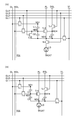
도 4는 화소의 구성예를 나타낸 회로도.
도 5는 화소의 구성예를 설명하기 위한 블록도.
도 6은 화소의 구성예를 나타낸 회로도.
도 7은 화소의 구성예를 나타낸 회로도.
도 8은 화소의 동작예를 나타낸 타이밍 차트.
도 9는 화소의 동작과 배선에 대한 전압 인가의 타이밍의 일례를 설명하기 위한 도면.
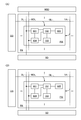
도 10은 표시부와 그 주변 회로의 구성예를 나타낸 블록도.
도 11은 표시 장치의 일례를 나타낸 상면도.
도 12는 터치 패널의 일례를 나타낸 사시도.
도 13은 표시 장치의 일례를 나타낸 단면도.
도 14는 트랜지스터의 구성예를 나타낸 단면도.
도 15는 트랜지스터의 구성예를 나타낸 단면도.
도 16은 전자 기기의 일례를 나타낸 사시도.
도 17은 전자 기기의 일례를 나타낸 사시도.
도 18은 문턱 전압의 보정에 따른 전류의 변화율을 나타낸 그래프.
도 19는 화상 데이터(전압)와 트랜지스터를 흐르는 전류량의 관계를 나타낸 그래프.
도 20은 트랜지스터의 드레인 전류와 게이트-소스 간 전압의 특성을 나타낸 그래프.
도 21은 시작(試作)한 표시 장치의 외관 사진.
| 화면 크기 | 8.65인치 |
| 화소수 | 1200×1920 |
| 화소 크기 | 96μm×96μm |
| 해상도 | 265ppi |
| 개구율 | 17.4% |
| 착색 방법 | 구분 형성 방식 |
| 발광 방식 | 톱 이미션 |
| 소스 드라이버 | COG |
| 스캔 드라이버 | 화소부와 동시에 형성 |
| 화상 데이터만 | 화상 데이터+보정 데이터 | |
| 휘도[cd/m2] | 801 | 1145 |
Claims (18)
- 반도체 장치로서,
화상 데이터 유지부와, 보정 데이터 유지부와, 구동 회로부와, 표시 소자와, 문턱 전압 보정 회로부를 포함하고,
상기 구동 회로부는 백 게이트를 갖는 제 1 트랜지스터를 포함하고,
상기 제 1 트랜지스터의 제 1 단자는 상기 표시 소자의 입력 단자에 전기적으로 접속되고,
상기 화상 데이터 유지부는 제 1 화상 데이터를 유지하는 기능을 갖고,
상기 보정 데이터 유지부는,
보정 데이터를 유지하는 기능과,
상기 화상 데이터 유지부가 상기 제 1 화상 데이터를 유지함으로써 상기 제 1 화상 데이터 및 상기 보정 데이터에 따른 제 2 화상 데이터를 생성하는 기능을 갖고,
상기 구동 회로부는 상기 제 1 트랜지스터의 게이트에 상기 제 2 화상 데이터에 따른 제 1 전위가 인가됨으로써, 상기 제 1 트랜지스터의 제 1 단자와 제 2 단자 간에서 제 1 전류를 생성하는 기능과, 상기 제 1 전류를 상기 표시 소자에 흘리는 기능을 갖고,
상기 문턱 전압 보정 회로부는 상기 구동 회로부에 포함되는 상기 제 1 트랜지스터의 문턱 전압을 보정하는 기능을 갖는, 반도체 장치. - 제 1 항에 있어서,
제 1 용량 소자 내지 제 3 용량 소자를 포함하고,
상기 화상 데이터 유지부는 제 2 트랜지스터를 포함하고,
상기 보정 데이터 유지부는 제 3 트랜지스터를 포함하고,
상기 문턱 전압 보정 회로는 제 4 트랜지스터를 포함하고,
상기 제 2 트랜지스터의 제 1 단자는 상기 제 1 용량 소자의 제 1 단자에 전기적으로 접속되고,
상기 제 3 트랜지스터의 제 1 단자는 상기 제 1 트랜지스터의 게이트와, 상기 제 1 용량 소자의 제 2 단자와, 상기 제 2 용량 소자의 제 1 단자에 전기적으로 접속되고,
상기 제 1 트랜지스터의 제 1 단자는 상기 제 2 용량 소자의 제 2 단자와 상기 제 3 용량 소자의 제 1 단자에 전기적으로 접속되고,
상기 제 1 트랜지스터의 백 게이트는 상기 제 4 트랜지스터의 제 1 단자와 상기 제 3 용량 소자의 제 2 단자에 전기적으로 접속되는, 반도체 장치. - 제 2 항에 있어서,
상기 제 1 트랜지스터 내지 상기 제 4 트랜지스터의 각각은 채널 형성 영역에 금속 산화물 및 실리콘 중 한쪽을 포함하는, 반도체 장치. - 제 2 항 또는 제 3 항에 있어서,
상기 구동 회로부는 제 5 트랜지스터를 포함하고,
상기 제 3 트랜지스터의 제 1 단자와 상기 표시 소자의 입력 단자는 상기 제 5 트랜지스터의 제 1 단자와 제 2 단자 간을 통하여 전기적으로 접속되는, 반도체 장치. - 제 4 항에 있어서,
상기 제 5 트랜지스터는 채널 형성 영역에 금속 산화물 및 실리콘 중 한쪽을 포함하는, 반도체 장치. - 제 2 항 내지 제 5 항 중 어느 한 항에 있어서,
제 6 트랜지스터를 포함하고,
상기 제 6 트랜지스터의 제 1 단자는 상기 제 1 트랜지스터의 게이트에 전기적으로 접속되고,
상기 제 6 트랜지스터의 제 2 단자는 상기 제 1 트랜지스터의 제 1 단자에 전기적으로 접속되는, 반도체 장치. - 제 6 항에 있어서,
상기 제 6 트랜지스터는 채널 형성 영역에 금속 산화물 및 실리콘 중 한쪽을 포함하는, 반도체 장치. - 제 2 항 내지 제 7 항 중 어느 한 항에 있어서,
제 1 기능 내지 제 3 기능을 갖고,
상기 제 1 기능은,
상기 제 3 트랜지스터를 온 상태로 하여 상기 제 1 트랜지스터의 게이트와, 상기 제 1 용량 소자의 제 2 단자와, 상기 제 2 용량 소자의 제 1 단자에 제 1 초기화 전위를 인가하는 기능과,
상기 제 4 트랜지스터를 온 상태로 하여 상기 제 1 트랜지스터의 백 게이트와 상기 제 3 용량 소자의 제 2 단자에 제 2 초기화 전위를 인가하는 기능과,
상기 제 1 트랜지스터의 제 1 단자와, 상기 제 2 용량 소자의 제 2 단자와, 상기 제 3 용량 소자의 제 1 단자에 제 3 초기화 전위를 인가하는 기능과,
상기 제 3 트랜지스터를 오프 상태로 하여 상기 제 2 용량 소자에 의하여 상기 제 1 초기화 전위와 상기 제 3 초기화 전위의 전위차를 유지하는 기능과,
상기 제 1 트랜지스터의 제 1 단자로부터 상기 표시 소자의 입력 단자로의 전류를 차단하고, 상기 제 1 트랜지스터의 제 1 단자와 제 2 단자 간에 전압을 인가하여 제 1 트랜지스터를 온 상태로 한 후, 상기 제 1 트랜지스터의 제 1 단자의 전위가 제 2 전위가 되고 제 1 트랜지스터가 오프 상태가 되었을 때, 상기 제 3 용량 소자에 의하여 상기 제 2 초기화 전위와 상기 제 2 전위의 전위차를 유지하는 기능을 갖고,
상기 제 2 기능은,
상기 제 3 트랜지스터를 온 상태로 하여 상기 제 1 트랜지스터의 게이트와, 상기 제 1 용량 소자의 제 2 단자와, 상기 제 2 용량 소자의 제 1 단자에 상기 보정 데이터에 따른 제 3 전위를 기록하는 기능과,
상기 제 3 트랜지스터를 오프 상태로 하여 상기 제 1 트랜지스터의 게이트와, 상기 제 1 용량 소자의 제 2 단자와, 상기 제 2 용량 소자의 제 1 단자에 의하여 상기 제 3 전위를 유지하는 기능을 갖고,
상기 제 3 기능은,
상기 제 2 트랜지스터를 온 상태로 하여 상기 제 1 용량 소자의 제 1 단자에 상기 제 1 화상 데이터에 따른 제 4 전위를 기록하는 기능과,
상기 제 1 용량 소자의 제 1 단자에 상기 제 4 전위가 기록됨으로써 상기 제 1 트랜지스터의 게이트와, 상기 제 1 용량 소자의 제 2 단자와, 상기 제 2 용량 소자의 제 1 단자에 유지된 상기 제 3 전위가 상기 제 2 화상 데이터에 따른 상기 제 1 전위로 변동하는 기능을 갖는, 반도체 장치. - 표시 장치로서,
제 1 항 내지 제 8 항 중 어느 한 항에 기재된 반도체 장치와, 주변 회로를 포함하는, 표시 장치. - 전자 기기로서,
제 9 항에 기재된 표시 장치와, 하우징을 포함하는, 전자 기기. - 반도체 장치의 동작 방법으로서,
화상 데이터 유지부와, 보정 데이터 유지부와, 구동 회로부와, 표시 소자와, 문턱 전압 보정 회로부를 포함하고,
상기 구동 회로부는 백 게이트를 갖는 제 1 트랜지스터를 포함하고,
상기 제 1 트랜지스터의 제 1 단자는 상기 표시 소자의 입력 단자에 전기적으로 접속되고,
상기 반도체 장치의 동작 방법은 문턱 전압 보정 기간과, 보정 데이터 기록 기간과, 화상 데이터 기록 기간과, 화상 표시 기간을 갖고,
상기 문턱 전압 보정 기간은 상기 문턱 전압 보정 회로부가 상기 제 1 트랜지스터의 백 게이트에 전위를 인가함으로써 상기 제 1 트랜지스터의 문턱 전압을 보정하는 기간을 갖고,
상기 보정 데이터 기록 기간은 상기 보정 데이터 유지부에 보정 데이터를 기록하는 기간을 갖고,
상기 화상 데이터 기록 기간은 상기 화상 데이터 유지부에 제 1 화상 데이터를 기록하고, 상기 보정 데이터 유지부가 상기 제 1 화상 데이터 및 상기 보정 데이터에 따른 제 2 화상 데이터를 생성하는 기간을 갖고,
상기 화상 표시 기간은 상기 제 1 트랜지스터의 게이트에 상기 제 2 화상 데이터에 따른 제 1 전위가 인가됨으로써 상기 구동 회로부가 상기 제 1 트랜지스터의 제 1 단자와 제 2 단자 간에서 제 1 전류를 생성하고, 상기 제 1 전류를 상기 표시 소자에 흘리는 기간을 갖는, 반도체 장치의 동작 방법. - 제 11 항에 있어서,
상기 반도체 장치의 동작 방법은 초기화 기간을 갖고,
상기 반도체 장치는 제 1 용량 소자 내지 제 3 용량 소자를 포함하고,
상기 화상 데이터 유지부는 제 2 트랜지스터를 포함하고,
상기 보정 데이터 유지부는 제 3 트랜지스터를 포함하고,
상기 문턱 전압 보정 회로는 제 4 트랜지스터를 포함하고,
상기 제 2 트랜지스터의 제 1 단자는 상기 제 1 용량 소자의 제 1 단자에 전기적으로 접속되고,
상기 제 3 트랜지스터의 제 1 단자는 상기 제 1 트랜지스터의 게이트와, 상기 제 1 용량 소자의 제 2 단자와, 상기 제 2 용량 소자의 제 1 단자에 전기적으로 접속되고,
상기 제 1 트랜지스터의 제 1 단자는 상기 제 2 용량 소자의 제 2 단자와, 상기 제 3 용량 소자의 제 1 단자와, 상기 표시 소자의 입력 단자에 전기적으로 접속되고,
상기 제 1 트랜지스터의 백 게이트는 상기 제 4 트랜지스터의 제 1 단자와, 상기 제 3 용량 소자의 제 2 단자에 전기적으로 접속되고,
상기 초기화 기간은,
상기 제 3 트랜지스터가 온 상태가 되어 상기 제 1 트랜지스터의 게이트와, 상기 제 1 용량 소자의 제 2 단자와, 상기 제 2 용량 소자의 제 1 단자에 제 1 초기화 전위가 인가되는 기간과,
상기 제 4 트랜지스터가 온 상태가 되어 상기 제 1 트랜지스터의 백 게이트와, 상기 제 3 용량 소자의 제 2 단자에 제 2 초기화 전위가 인가되는 기간과,
상기 제 1 트랜지스터의 제 1 단자와, 상기 제 2 용량 소자의 제 2 단자와, 상기 제 3 용량 소자의 제 1 단자에 제 3 초기화 전위가 인가되는 기간을 갖고,
상기 문턱 전압 보정 기간은,
상기 제 1 트랜지스터의 제 1 단자로부터 표시 소자로의 전류를 차단하는 기간과,
상기 제 3 트랜지스터가 오프 상태가 되어 상기 제 2 용량 소자가 상기 제 1 초기화 전위와 상기 제 3 초기화 전위의 전위차를 유지하는 기간과,
상기 제 1 트랜지스터의 제 2 단자에 고전위가 인가됨으로써 상기 제 1 트랜지스터의 제 1 단자의 전위가 상기 제 1 트랜지스터가 오프 상태가 되는 제 2 전위에 달할 때까지 상기 제 1 트랜지스터의 제 1 단자와 제 2 단자 간에 제 2 전류가 흐르는 기간과,
상기 제 4 트랜지스터가 오프 상태가 되어 상기 제 3 용량 소자가 상기 제 2 전위와 상기 제 2 초기화 전위의 전위차를 유지하는 기간을 갖고,
상기 보정 데이터 기록 기간은,
상기 제 3 트랜지스터가 온 상태가 되어 상기 제 1 트랜지스터의 게이트와, 상기 제 1 용량 소자의 제 2 단자와, 상기 제 2 용량 소자의 제 1 단자에 상기 보정 데이터에 따른 제 3 전위가 인가되는 기간과,
상기 제 3 트랜지스터가 오프 상태가 되어 상기 제 1 트랜지스터의 게이트와, 상기 제 1 용량 소자의 제 2 단자와, 상기 제 2 용량 소자의 제 1 단자에 의하여 상기 제 3 전위가 유지되는 기간을 갖고,
상기 화상 데이터 기록 기간은,
상기 제 2 트랜지스터가 온 상태가 되어 상기 제 1 용량 소자의 제 1 단자에 상기 제 1 화상 데이터에 따른 제 4 전위가 인가되는 기간과,
상기 제 1 용량 소자의 제 1 단자에 상기 제 4 전위가 기록됨으로써 상기 제 1 트랜지스터의 게이트와, 상기 제 1 용량 소자의 제 2 단자와, 상기 제 2 용량 소자의 제 1 단자에 유지된 상기 제 3 전위가 상기 제 2 화상 데이터에 따른 상기 제 1 전위로 변동하는 기간을 갖는, 반도체 장치의 동작 방법. - 제 12 항에 있어서,
상기 제 1 트랜지스터 내지 상기 제 4 트랜지스터의 각각은 채널 형성 영역에 금속 산화물 및 실리콘 중 한쪽을 포함하는, 표시 장치의 동작 방법. - 제 12 항 또는 제 13 항에 있어서,
상기 구동 회로부는 제 5 트랜지스터를 포함하고,
상기 제 3 트랜지스터의 제 1 단자와 상기 표시 소자의 입력 단자는 상기 제 5 트랜지스터의 제 1 단자와 제 2 단자 간을 통하여 전기적으로 접속되고,
상기 초기화 기간과, 상기 보정 데이터 기록 기간과, 상기 화상 데이터 기록 기간은 상기 제 5 트랜지스터가 오프 상태가 되는 기간을 갖고,
상기 화상 표시 기간은 상기 제 5 트랜지스터가 온 상태가 되는 기간을 갖는, 반도체 장치의 동작 방법. - 제 14 항에 있어서,
상기 제 5 트랜지스터는 채널 형성 영역에 금속 산화물 및 실리콘 중 한쪽을 포함하는, 반도체 장치의 동작 방법. - 제 12 항 내지 제 15 항 중 어느 한 항에 있어서,
상기 반도체 장치는 제 6 트랜지스터를 포함하고,
상기 제 6 트랜지스터의 제 1 단자는 상기 제 1 트랜지스터의 게이트에 전기적으로 접속되고,
상기 제 6 트랜지스터의 제 2 단자는 상기 제 1 트랜지스터의 제 1 단자에 전기적으로 접속되고,
상기 문턱 전압 보정 기간은 상기 제 6 트랜지스터가 온 상태가 되는 기간을 갖는, 반도체 장치의 동작 방법. - 제 16 항에 있어서,
상기 제 6 트랜지스터는 채널 형성 영역에 금속 산화물 및 실리콘 중 한쪽을 포함하는, 반도체 장치의 동작 방법. - 표시 장치의 동작 방법으로서,
제 11 항 내지 제 17 항 중 어느 한 항에 기재된 반도체 장치의 동작 방법을 포함하는 표시 장치의 동작 방법이고,
상기 표시 장치는 복수의 상기 반도체 장치가 매트릭스상으로 배치된 표시부를 갖고,
상기 복수의 상기 반도체 장치의 일부는 제 1 화소 및 제 2 화소로서 기능하고,
상기 제 1 화소와 상기 제 2 화소는 상기 표시부에서 서로 상이한 행에 위치하고,
상기 제 1 화소가 상기 문턱 전압 보정 기간의 동작을 수행할 때, 상기 제 2 화소는 상기 보정 데이터 기록 기간 및 상기 화상 데이터 기록 기간의 각각의 동작을 수행하는, 표시 장치의 동작 방법.
Priority Applications (1)
| Application Number | Priority Date | Filing Date | Title |
|---|---|---|---|
| KR1020247003788A KR102886109B1 (ko) | 2017-12-06 | 2018-12-04 | 반도체 장치, 표시 장치, 전자 기기, 및 동작 방법 |
Applications Claiming Priority (7)
| Application Number | Priority Date | Filing Date | Title |
|---|---|---|---|
| JPJP-P-2017-233931 | 2017-12-06 | ||
| JP2017233931 | 2017-12-06 | ||
| JPJP-P-2018-020851 | 2018-02-08 | ||
| JP2018020851 | 2018-02-08 | ||
| JPJP-P-2018-224142 | 2018-11-29 | ||
| JP2018224142 | 2018-11-29 | ||
| PCT/IB2018/059593 WO2019111137A1 (ja) | 2017-12-06 | 2018-12-04 | 半導体装置、表示装置、電子機器、及び動作方法 |
Related Child Applications (1)
| Application Number | Title | Priority Date | Filing Date |
|---|---|---|---|
| KR1020247003788A Division KR102886109B1 (ko) | 2017-12-06 | 2018-12-04 | 반도체 장치, 표시 장치, 전자 기기, 및 동작 방법 |
Publications (2)
| Publication Number | Publication Date |
|---|---|
| KR20200096237A true KR20200096237A (ko) | 2020-08-11 |
| KR102633768B1 KR102633768B1 (ko) | 2024-02-06 |
Family
ID=66750156
Family Applications (3)
| Application Number | Title | Priority Date | Filing Date |
|---|---|---|---|
| KR1020257037686A Pending KR20250162955A (ko) | 2017-12-06 | 2018-12-04 | 반도체 장치, 표시 장치, 전자 기기, 및 동작 방법 |
| KR1020207017275A Active KR102633768B1 (ko) | 2017-12-06 | 2018-12-04 | 반도체 장치, 표시 장치, 전자 기기, 및 동작 방법 |
| KR1020247003788A Active KR102886109B1 (ko) | 2017-12-06 | 2018-12-04 | 반도체 장치, 표시 장치, 전자 기기, 및 동작 방법 |
Family Applications Before (1)
| Application Number | Title | Priority Date | Filing Date |
|---|---|---|---|
| KR1020257037686A Pending KR20250162955A (ko) | 2017-12-06 | 2018-12-04 | 반도체 장치, 표시 장치, 전자 기기, 및 동작 방법 |
Family Applications After (1)
| Application Number | Title | Priority Date | Filing Date |
|---|---|---|---|
| KR1020247003788A Active KR102886109B1 (ko) | 2017-12-06 | 2018-12-04 | 반도체 장치, 표시 장치, 전자 기기, 및 동작 방법 |
Country Status (5)
| Country | Link |
|---|---|
| US (1) | US11417273B2 (ko) |
| JP (5) | JP7184491B2 (ko) |
| KR (3) | KR20250162955A (ko) |
| CN (1) | CN111406280B (ko) |
| WO (1) | WO2019111137A1 (ko) |
Cited By (3)
| Publication number | Priority date | Publication date | Assignee | Title |
|---|---|---|---|---|
| KR20220055554A (ko) * | 2020-10-26 | 2022-05-04 | 삼성디스플레이 주식회사 | 화소 회로, 이를 포함하는 표시 장치 및 화소 회로의 구동 방법 |
| US12223904B2 (en) | 2021-06-30 | 2025-02-11 | Semiconductor Energy Laboratory Co., Ltd. | Semiconductor device and method for driving semiconductor device |
| US12555529B2 (en) | 2021-10-27 | 2026-02-17 | Semiconductor Energy Laboratory Co., Ltd. | Display apparatus and electronic device |
Families Citing this family (31)
| Publication number | Priority date | Publication date | Assignee | Title |
|---|---|---|---|---|
| WO2019111137A1 (ja) * | 2017-12-06 | 2019-06-13 | 株式会社半導体エネルギー研究所 | 半導体装置、表示装置、電子機器、及び動作方法 |
| US11120764B2 (en) | 2017-12-21 | 2021-09-14 | Semiconductor Energy Laboratory Co., Ltd. | Display device and electronic device |
| WO2020053693A1 (ja) | 2018-09-12 | 2020-03-19 | 株式会社半導体エネルギー研究所 | 表示装置の動作方法 |
| JP7412360B2 (ja) | 2019-02-05 | 2024-01-12 | 株式会社半導体エネルギー研究所 | 表示装置および電子機器 |
| US11915647B2 (en) * | 2019-10-02 | 2024-02-27 | Shar Kabushiki Kaisha | Display device equipped with current-driven electro-optical elements |
| US20210193049A1 (en) | 2019-12-23 | 2021-06-24 | Apple Inc. | Electronic Display with In-Pixel Compensation and Oxide Drive Transistors |
| US12426467B2 (en) | 2019-12-25 | 2025-09-23 | Semiconductor Energy Laboratory Co., Ltd. | Display apparatus and electronic device comprising first capacitor and second capacitor |
| KR20210102557A (ko) * | 2020-02-11 | 2021-08-20 | 삼성디스플레이 주식회사 | 디스플레이 장치 |
| CN111402816A (zh) * | 2020-04-14 | 2020-07-10 | 深圳市华星光电半导体显示技术有限公司 | 一种像素电路和具有该像素电路的amoled显示面板 |
| KR20230047392A (ko) * | 2020-08-03 | 2023-04-07 | 가부시키가이샤 한도오따이 에네루기 켄큐쇼 | 반도체 장치 및 전자 기기 |
| TWI907464B (zh) | 2020-08-12 | 2025-12-11 | 日商半導體能源研究所股份有限公司 | 顯示裝置、其工作方法以及電子裝置 |
| WO2022219447A1 (ja) * | 2021-04-16 | 2022-10-20 | 株式会社半導体エネルギー研究所 | 表示装置 |
| CN113270067B (zh) | 2021-06-28 | 2022-05-03 | 深圳市华星光电半导体显示技术有限公司 | 像素电路及显示面板 |
| US12300174B2 (en) * | 2021-08-12 | 2025-05-13 | Semiconductor Energy Laboratory Co., Ltd. | Correction method of display apparatus including pixel and plurality of circuits |
| WO2023037203A1 (ja) * | 2021-09-10 | 2023-03-16 | 株式会社半導体エネルギー研究所 | 半導体装置 |
| US12327519B2 (en) * | 2021-09-14 | 2025-06-10 | Apple Inc. | Electronic devices with displays for mitigating cathode noise |
| WO2023043579A1 (en) * | 2021-09-14 | 2023-03-23 | Apple Inc. | Electronic devices with displays for mitigating cathode noise |
| CN115909970B (zh) | 2021-09-30 | 2026-02-17 | 昆山国显光电有限公司 | 像素电路及其驱动方法和显示面板 |
| KR102862796B1 (ko) * | 2021-12-16 | 2025-09-22 | 엘지디스플레이 주식회사 | 전계 발광 표시장치 |
| US12482415B2 (en) | 2021-12-22 | 2025-11-25 | Semiconductor Energy Laboratory Co., Ltd. | Display apparatus and electronic device |
| KR102871988B1 (ko) * | 2021-12-23 | 2025-10-16 | 삼성전자주식회사 | 적층형 디스플레이 구동 집적 회로 및 이를 포함하는 디스플레이 장치 |
| CN115116395B (zh) * | 2022-07-15 | 2024-12-17 | 惠州华星光电显示有限公司 | 驱动电路、驱动方法及显示面板 |
| CN115565482A (zh) * | 2022-10-10 | 2023-01-03 | 深圳市华星光电半导体显示技术有限公司 | 补偿电路、驱动方法及显示面板 |
| US20240188330A1 (en) * | 2022-12-01 | 2024-06-06 | Semiconductor Energy Laboratory Co., Ltd. | Semiconductor device, display apparatus, and driving method of semiconductor device |
| CN116206546A (zh) * | 2023-03-02 | 2023-06-02 | 合肥维信诺科技有限公司 | 一种像素电路及显示面板 |
| KR20240144520A (ko) * | 2023-03-22 | 2024-10-02 | 삼성디스플레이 주식회사 | 표시 장치 및 이를 포함하는 전자 장치 |
| KR20240172347A (ko) * | 2023-05-31 | 2024-12-10 | 삼성디스플레이 주식회사 | 화소 및 이를 구비하는 표시 장치 |
| KR20250004433A (ko) * | 2023-06-29 | 2025-01-08 | 삼성디스플레이 주식회사 | 화소 및 그것을 포함하는 표시 장치 |
| KR20250027298A (ko) * | 2023-08-16 | 2025-02-26 | 삼성디스플레이 주식회사 | 표시 장치 |
| KR20250176187A (ko) | 2024-06-11 | 2025-12-19 | 삼성디스플레이 주식회사 | 화소 및 이를 구비하는 표시 장치 |
| CN119446059B (zh) * | 2024-11-29 | 2025-08-01 | 惠科股份有限公司 | 像素驱动电路、像素驱动方法和显示面板 |
Citations (4)
| Publication number | Priority date | Publication date | Assignee | Title |
|---|---|---|---|---|
| JP2010156963A (ja) | 2008-12-05 | 2010-07-15 | Semiconductor Energy Lab Co Ltd | 半導体装置 |
| KR20150046022A (ko) * | 2012-08-31 | 2015-04-29 | 소니 주식회사 | 표시 장치 및 전자 기기 |
| KR20150068909A (ko) * | 2013-12-12 | 2015-06-22 | 가부시키가이샤 한도오따이 에네루기 켄큐쇼 | 발광 장치 |
| JP2017010000A (ja) | 2015-04-13 | 2017-01-12 | 株式会社半導体エネルギー研究所 | 表示装置 |
Family Cites Families (43)
| Publication number | Priority date | Publication date | Assignee | Title |
|---|---|---|---|---|
| JP2008134625A (ja) * | 2006-10-26 | 2008-06-12 | Semiconductor Energy Lab Co Ltd | 半導体装置、表示装置及び電子機器 |
| JP5045323B2 (ja) * | 2007-09-14 | 2012-10-10 | セイコーエプソン株式会社 | 電気光学装置、電気光学装置の制御方法および電子機器 |
| JP2009300752A (ja) * | 2008-06-13 | 2009-12-24 | Fujifilm Corp | 表示装置及び駆動方法 |
| JP5207885B2 (ja) | 2008-09-03 | 2013-06-12 | キヤノン株式会社 | 画素回路、発光表示装置及びそれらの駆動方法 |
| JP5251420B2 (ja) | 2008-10-23 | 2013-07-31 | セイコーエプソン株式会社 | 発光装置および電子機器、発光装置の駆動方法 |
| KR100989126B1 (ko) | 2009-02-05 | 2010-10-20 | 삼성모바일디스플레이주식회사 | 전자 영상 기기 및 그 구동 방법 |
| KR101125571B1 (ko) | 2010-02-05 | 2012-03-22 | 삼성모바일디스플레이주식회사 | 화소, 이를 이용한 표시 장치 및 그 구동 방법 |
| JP5804732B2 (ja) | 2011-03-04 | 2015-11-04 | 株式会社Joled | 駆動方法、表示装置および電子機器 |
| KR20120110387A (ko) | 2011-03-29 | 2012-10-10 | 삼성전자주식회사 | 화소 회로 및 화소 회로의 구동 방법 |
| KR20140051268A (ko) * | 2011-07-22 | 2014-04-30 | 가부시키가이샤 한도오따이 에네루기 켄큐쇼 | 발광 장치 |
| JP6099336B2 (ja) * | 2011-09-14 | 2017-03-22 | 株式会社半導体エネルギー研究所 | 発光装置 |
| JP5832399B2 (ja) * | 2011-09-16 | 2015-12-16 | 株式会社半導体エネルギー研究所 | 発光装置 |
| KR101463651B1 (ko) * | 2011-10-12 | 2014-11-20 | 엘지디스플레이 주식회사 | 유기발광 표시장치 |
| WO2013137014A1 (en) * | 2012-03-13 | 2013-09-19 | Semiconductor Energy Laboratory Co., Ltd. | Light-emitting device and method for driving the same |
| JP6158588B2 (ja) * | 2012-05-31 | 2017-07-05 | 株式会社半導体エネルギー研究所 | 発光装置 |
| KR20140050361A (ko) * | 2012-10-19 | 2014-04-29 | 삼성디스플레이 주식회사 | 화소, 이를 이용한 입체 영상 표시 장치 및 그의 구동 방법 |
| JP2014219440A (ja) | 2013-05-01 | 2014-11-20 | 三星ディスプレイ株式會社Samsung Display Co.,Ltd. | 映像表示装置及び画素回路の制御方法 |
| KR102099709B1 (ko) * | 2013-06-19 | 2020-04-13 | 삼성디스플레이 주식회사 | 표시 패널 구동부, 이를 이용한 표시 패널 구동 방법 및 이를 포함하는 표시 장치 |
| JP6495602B2 (ja) * | 2013-09-13 | 2019-04-03 | 株式会社半導体エネルギー研究所 | 発光装置 |
| JP6619137B2 (ja) * | 2013-12-06 | 2019-12-11 | 株式会社半導体エネルギー研究所 | 発光装置 |
| KR102091485B1 (ko) | 2013-12-30 | 2020-03-20 | 엘지디스플레이 주식회사 | 유기 발광 표시 장치 및 그의 구동 방법 |
| TWI654613B (zh) * | 2014-02-21 | 2019-03-21 | 日商半導體能源研究所股份有限公司 | 半導體裝置及電子裝置 |
| KR102213736B1 (ko) * | 2014-04-15 | 2021-02-09 | 삼성디스플레이 주식회사 | 유기 발광 표시 장치 및 이의 구동 방법 |
| CN104064149B (zh) * | 2014-07-07 | 2016-07-06 | 深圳市华星光电技术有限公司 | 像素电路、具备该像素电路的显示面板和显示器 |
| WO2016034984A1 (en) * | 2014-09-05 | 2016-03-10 | Semiconductor Energy Laboratory Co., Ltd. | Semiconductor device, driver ic, display device, and electronic device |
| KR102230928B1 (ko) * | 2014-10-13 | 2021-03-24 | 삼성디스플레이 주식회사 | 유기 발광 표시 장치 및 이의 구동 방법 |
| KR20160048640A (ko) * | 2014-10-23 | 2016-05-04 | 삼성디스플레이 주식회사 | 표시 장치, 화소 회로, 및 표시 장치의 제어 방법 |
| KR102285393B1 (ko) * | 2015-03-13 | 2021-08-04 | 삼성디스플레이 주식회사 | 유기 발광 표시 장치 및 이의 구동 방법 |
| WO2016151429A1 (en) | 2015-03-23 | 2016-09-29 | Semiconductor Energy Laboratory Co., Ltd. | Display panel and information processing device |
| US10170565B2 (en) * | 2015-04-22 | 2019-01-01 | Semiconductor Energy Laboratory Co., Ltd. | Imaging device, method for driving imaging device, and electronic device |
| KR102376409B1 (ko) * | 2015-07-28 | 2022-03-22 | 삼성디스플레이 주식회사 | 유기전계발광 표시장치 및 그의 구동방법 |
| JP6660155B2 (ja) | 2015-11-13 | 2020-03-04 | 株式会社Joled | 表示装置および電子機器 |
| US9818344B2 (en) | 2015-12-04 | 2017-11-14 | Apple Inc. | Display with light-emitting diodes |
| KR20180095836A (ko) * | 2015-12-18 | 2018-08-28 | 가부시키가이샤 한도오따이 에네루기 켄큐쇼 | 반도체 장치 및 상기 반도체 장치를 포함한 표시 장치 |
| KR102460302B1 (ko) * | 2015-12-31 | 2022-10-27 | 엘지디스플레이 주식회사 | 유기발광소자 표시장치 및 이의 구동방법 |
| KR102488767B1 (ko) * | 2016-02-01 | 2023-01-17 | 삼성디스플레이 주식회사 | 정전 방지 회로 및 이를 포함하는 표시 장치 |
| US10528165B2 (en) | 2016-04-04 | 2020-01-07 | Semiconductor Energy Laboratory Co., Ltd. | Display device, display module, and electronic device |
| JP6315072B2 (ja) | 2016-12-07 | 2018-04-25 | セイコーエプソン株式会社 | 電気光学装置及び電子機器 |
| CN106652918A (zh) | 2017-03-20 | 2017-05-10 | 京东方科技集团股份有限公司 | 一种goa单元及其驱动方法、goa电路、显示装置 |
| WO2019043483A1 (en) | 2017-08-31 | 2019-03-07 | Semiconductor Energy Laboratory Co., Ltd. | DISPLAY DEVICE AND ELECTRONIC DEVICE |
| US11302278B2 (en) | 2017-09-15 | 2022-04-12 | Semiconductor Energy Laboratory Co., Ltd. | Display device including pixel and electronic device |
| JP7225112B2 (ja) | 2017-11-09 | 2023-02-20 | 株式会社半導体エネルギー研究所 | 表示装置、電子機器 |
| WO2019111137A1 (ja) | 2017-12-06 | 2019-06-13 | 株式会社半導体エネルギー研究所 | 半導体装置、表示装置、電子機器、及び動作方法 |
-
2018
- 2018-12-04 WO PCT/IB2018/059593 patent/WO2019111137A1/ja not_active Ceased
- 2018-12-04 KR KR1020257037686A patent/KR20250162955A/ko active Pending
- 2018-12-04 JP JP2019557709A patent/JP7184491B2/ja active Active
- 2018-12-04 US US16/765,496 patent/US11417273B2/en active Active
- 2018-12-04 KR KR1020207017275A patent/KR102633768B1/ko active Active
- 2018-12-04 KR KR1020247003788A patent/KR102886109B1/ko active Active
- 2018-12-04 CN CN201880077322.2A patent/CN111406280B/zh not_active Expired - Fee Related
-
2022
- 2022-11-23 JP JP2022186968A patent/JP7340672B2/ja active Active
-
2023
- 2023-08-28 JP JP2023138020A patent/JP7546124B2/ja active Active
-
2024
- 2024-08-26 JP JP2024144232A patent/JP7766149B2/ja active Active
-
2025
- 2025-10-27 JP JP2025180399A patent/JP2026016597A/ja active Pending
Patent Citations (4)
| Publication number | Priority date | Publication date | Assignee | Title |
|---|---|---|---|---|
| JP2010156963A (ja) | 2008-12-05 | 2010-07-15 | Semiconductor Energy Lab Co Ltd | 半導体装置 |
| KR20150046022A (ko) * | 2012-08-31 | 2015-04-29 | 소니 주식회사 | 표시 장치 및 전자 기기 |
| KR20150068909A (ko) * | 2013-12-12 | 2015-06-22 | 가부시키가이샤 한도오따이 에네루기 켄큐쇼 | 발광 장치 |
| JP2017010000A (ja) | 2015-04-13 | 2017-01-12 | 株式会社半導体エネルギー研究所 | 表示装置 |
Non-Patent Citations (8)
| Title |
|---|
| K. Kato et al., "Japanese Journal of Applied Physics", 2012, volume 51, p.021201-1-021201-7 |
| S. Amano et al., "SID Symposium Digest of Technical Papers", 2010, volume 41, issue 1, p.626-629 |
| S. Ito et al., "The Proceedings of AM-FPD'13 Digest of Technical Papers", 2013, p.151-154 |
| S. Matsuda et al., "2015 Symposium on VLSI Technology Digest of Technical Papers", 2015, p.T216-T217 |
| S. Yamazaki et al., "ECS Journal of Solid State Science and Technology", 2014, volume 3, issue 9, p.Q3012-Q3022 |
| S. Yamazaki et al., "Japanese Journal of Applied Physics", 2014, volume 53, Number 4S, p.04ED18-1-04ED18-10 |
| S. Yamazaki et al., "SID Symposium Digest of Technical Papers", 2012, volume 43, issue 1, p.183-186 |
| S. Yamazaki, "ECS Transactions", 2014, volume 64, issue 10, p.155-164 |
Cited By (3)
| Publication number | Priority date | Publication date | Assignee | Title |
|---|---|---|---|---|
| KR20220055554A (ko) * | 2020-10-26 | 2022-05-04 | 삼성디스플레이 주식회사 | 화소 회로, 이를 포함하는 표시 장치 및 화소 회로의 구동 방법 |
| US12223904B2 (en) | 2021-06-30 | 2025-02-11 | Semiconductor Energy Laboratory Co., Ltd. | Semiconductor device and method for driving semiconductor device |
| US12555529B2 (en) | 2021-10-27 | 2026-02-17 | Semiconductor Energy Laboratory Co., Ltd. | Display apparatus and electronic device |
Also Published As
| Publication number | Publication date |
|---|---|
| KR20250162955A (ko) | 2025-11-19 |
| JP2023169176A (ja) | 2023-11-29 |
| JP7184491B2 (ja) | 2022-12-06 |
| US20200320930A1 (en) | 2020-10-08 |
| JP7766149B2 (ja) | 2025-11-07 |
| KR102886109B1 (ko) | 2025-11-14 |
| JP7340672B2 (ja) | 2023-09-07 |
| WO2019111137A1 (ja) | 2019-06-13 |
| JP2023024459A (ja) | 2023-02-16 |
| JP2024164190A (ja) | 2024-11-26 |
| CN111406280A (zh) | 2020-07-10 |
| CN111406280B (zh) | 2022-12-06 |
| KR102633768B1 (ko) | 2024-02-06 |
| JP2026016597A (ja) | 2026-02-03 |
| US11417273B2 (en) | 2022-08-16 |
| KR20240018693A (ko) | 2024-02-13 |
| JPWO2019111137A1 (ja) | 2021-01-14 |
| JP7546124B2 (ja) | 2024-09-05 |
Similar Documents
| Publication | Publication Date | Title |
|---|---|---|
| JP7340672B2 (ja) | 表示装置 | |
| US11876098B2 (en) | Display device having a plurality of transistors | |
| KR102881123B1 (ko) | 표시 장치 및 전자 기기 | |
| JP7700318B2 (ja) | 表示装置 | |
| JP2019086780A (ja) | 半導体装置、表示装置、及び電子機器 | |
| US11100855B2 (en) | Display device and electronic device |
Legal Events
| Date | Code | Title | Description |
|---|---|---|---|
| PA0105 | International application |
Patent event date: 20200616 Patent event code: PA01051R01D Comment text: International Patent Application |
|
| PG1501 | Laying open of application | ||
| PA0201 | Request for examination |
Patent event code: PA02012R01D Patent event date: 20211015 Comment text: Request for Examination of Application |
|
| E902 | Notification of reason for refusal | ||
| PE0902 | Notice of grounds for rejection |
Comment text: Notification of reason for refusal Patent event date: 20230221 Patent event code: PE09021S01D |
|
| E701 | Decision to grant or registration of patent right | ||
| PE0701 | Decision of registration |
Patent event code: PE07011S01D Comment text: Decision to Grant Registration Patent event date: 20231030 |
|
| A107 | Divisional application of patent | ||
| GRNT | Written decision to grant | ||
| PA0104 | Divisional application for international application |
Comment text: Divisional Application for International Patent Patent event code: PA01041R01D Patent event date: 20240131 |
|
| PR0701 | Registration of establishment |
Comment text: Registration of Establishment Patent event date: 20240131 Patent event code: PR07011E01D |
|
| PR1002 | Payment of registration fee |
Payment date: 20240201 End annual number: 3 Start annual number: 1 |
|
| PG1601 | Publication of registration |