KR20200096357A - Display device and manufacturing method thereof - Google Patents
Display device and manufacturing method thereof Download PDFInfo
- Publication number
- KR20200096357A KR20200096357A KR1020190013736A KR20190013736A KR20200096357A KR 20200096357 A KR20200096357 A KR 20200096357A KR 1020190013736 A KR1020190013736 A KR 1020190013736A KR 20190013736 A KR20190013736 A KR 20190013736A KR 20200096357 A KR20200096357 A KR 20200096357A
- Authority
- KR
- South Korea
- Prior art keywords
- color filter
- spacer
- electrode
- blocking member
- light blocking
- Prior art date
- Legal status (The legal status is an assumption and is not a legal conclusion. Google has not performed a legal analysis and makes no representation as to the accuracy of the status listed.)
- Granted
Links
Images










Classifications
-
- H01L27/322—
-
- G—PHYSICS
- G06—COMPUTING OR CALCULATING; COUNTING
- G06F—ELECTRIC DIGITAL DATA PROCESSING
- G06F3/00—Input arrangements for transferring data to be processed into a form capable of being handled by the computer; Output arrangements for transferring data from processing unit to output unit, e.g. interface arrangements
- G06F3/01—Input arrangements or combined input and output arrangements for interaction between user and computer
- G06F3/03—Arrangements for converting the position or the displacement of a member into a coded form
- G06F3/041—Digitisers, e.g. for touch screens or touch pads, characterised by the transducing means
- G06F3/044—Digitisers, e.g. for touch screens or touch pads, characterised by the transducing means by capacitive means
- G06F3/0446—Digitisers, e.g. for touch screens or touch pads, characterised by the transducing means by capacitive means using a grid-like structure of electrodes in at least two directions, e.g. using row and column electrodes
-
- G—PHYSICS
- G06—COMPUTING OR CALCULATING; COUNTING
- G06F—ELECTRIC DIGITAL DATA PROCESSING
- G06F3/00—Input arrangements for transferring data to be processed into a form capable of being handled by the computer; Output arrangements for transferring data from processing unit to output unit, e.g. interface arrangements
- G06F3/01—Input arrangements or combined input and output arrangements for interaction between user and computer
- G06F3/03—Arrangements for converting the position or the displacement of a member into a coded form
- G06F3/041—Digitisers, e.g. for touch screens or touch pads, characterised by the transducing means
- G06F3/0412—Digitisers structurally integrated in a display
-
- G—PHYSICS
- G06—COMPUTING OR CALCULATING; COUNTING
- G06F—ELECTRIC DIGITAL DATA PROCESSING
- G06F3/00—Input arrangements for transferring data to be processed into a form capable of being handled by the computer; Output arrangements for transferring data from processing unit to output unit, e.g. interface arrangements
- G06F3/01—Input arrangements or combined input and output arrangements for interaction between user and computer
- G06F3/03—Arrangements for converting the position or the displacement of a member into a coded form
- G06F3/041—Digitisers, e.g. for touch screens or touch pads, characterised by the transducing means
- G06F3/044—Digitisers, e.g. for touch screens or touch pads, characterised by the transducing means by capacitive means
-
- H01L27/3211—
-
- H01L27/3244—
-
- H01L27/3246—
-
- H01L51/5284—
-
- H01L51/56—
-
- H—ELECTRICITY
- H10—SEMICONDUCTOR DEVICES; ELECTRIC SOLID-STATE DEVICES NOT OTHERWISE PROVIDED FOR
- H10K—ORGANIC ELECTRIC SOLID-STATE DEVICES
- H10K50/00—Organic light-emitting devices
- H10K50/10—OLEDs or polymer light-emitting diodes [PLED]
- H10K50/11—OLEDs or polymer light-emitting diodes [PLED] characterised by the electroluminescent [EL] layers
- H10K50/125—OLEDs or polymer light-emitting diodes [PLED] characterised by the electroluminescent [EL] layers specially adapted for multicolour light emission, e.g. for emitting white light
- H10K50/13—OLEDs or polymer light-emitting diodes [PLED] characterised by the electroluminescent [EL] layers specially adapted for multicolour light emission, e.g. for emitting white light comprising stacked EL layers within one EL unit
- H10K50/131—OLEDs or polymer light-emitting diodes [PLED] characterised by the electroluminescent [EL] layers specially adapted for multicolour light emission, e.g. for emitting white light comprising stacked EL layers within one EL unit with spacer layers between the electroluminescent layers
-
- H—ELECTRICITY
- H10—SEMICONDUCTOR DEVICES; ELECTRIC SOLID-STATE DEVICES NOT OTHERWISE PROVIDED FOR
- H10K—ORGANIC ELECTRIC SOLID-STATE DEVICES
- H10K59/00—Integrated devices, or assemblies of multiple devices, comprising at least one organic light-emitting element covered by group H10K50/00
- H10K59/10—OLED displays
- H10K59/12—Active-matrix OLED [AMOLED] displays
- H10K59/121—Active-matrix OLED [AMOLED] displays characterised by the geometry or disposition of pixel elements
- H10K59/1213—Active-matrix OLED [AMOLED] displays characterised by the geometry or disposition of pixel elements the pixel elements being TFTs
-
- H—ELECTRICITY
- H10—SEMICONDUCTOR DEVICES; ELECTRIC SOLID-STATE DEVICES NOT OTHERWISE PROVIDED FOR
- H10K—ORGANIC ELECTRIC SOLID-STATE DEVICES
- H10K59/00—Integrated devices, or assemblies of multiple devices, comprising at least one organic light-emitting element covered by group H10K50/00
- H10K59/10—OLED displays
- H10K59/12—Active-matrix OLED [AMOLED] displays
- H10K59/122—Pixel-defining structures or layers, e.g. banks
-
- H—ELECTRICITY
- H10—SEMICONDUCTOR DEVICES; ELECTRIC SOLID-STATE DEVICES NOT OTHERWISE PROVIDED FOR
- H10K—ORGANIC ELECTRIC SOLID-STATE DEVICES
- H10K59/00—Integrated devices, or assemblies of multiple devices, comprising at least one organic light-emitting element covered by group H10K50/00
- H10K59/10—OLED displays
- H10K59/12—Active-matrix OLED [AMOLED] displays
- H10K59/131—Interconnections, e.g. wiring lines or terminals
-
- H—ELECTRICITY
- H10—SEMICONDUCTOR DEVICES; ELECTRIC SOLID-STATE DEVICES NOT OTHERWISE PROVIDED FOR
- H10K—ORGANIC ELECTRIC SOLID-STATE DEVICES
- H10K59/00—Integrated devices, or assemblies of multiple devices, comprising at least one organic light-emitting element covered by group H10K50/00
- H10K59/30—Devices specially adapted for multicolour light emission
- H10K59/35—Devices specially adapted for multicolour light emission comprising red-green-blue [RGB] subpixels
-
- H—ELECTRICITY
- H10—SEMICONDUCTOR DEVICES; ELECTRIC SOLID-STATE DEVICES NOT OTHERWISE PROVIDED FOR
- H10K—ORGANIC ELECTRIC SOLID-STATE DEVICES
- H10K59/00—Integrated devices, or assemblies of multiple devices, comprising at least one organic light-emitting element covered by group H10K50/00
- H10K59/30—Devices specially adapted for multicolour light emission
- H10K59/38—Devices specially adapted for multicolour light emission comprising colour filters or colour changing media [CCM]
-
- H—ELECTRICITY
- H10—SEMICONDUCTOR DEVICES; ELECTRIC SOLID-STATE DEVICES NOT OTHERWISE PROVIDED FOR
- H10K—ORGANIC ELECTRIC SOLID-STATE DEVICES
- H10K59/00—Integrated devices, or assemblies of multiple devices, comprising at least one organic light-emitting element covered by group H10K50/00
- H10K59/40—OLEDs integrated with touch screens
-
- H—ELECTRICITY
- H10—SEMICONDUCTOR DEVICES; ELECTRIC SOLID-STATE DEVICES NOT OTHERWISE PROVIDED FOR
- H10K—ORGANIC ELECTRIC SOLID-STATE DEVICES
- H10K59/00—Integrated devices, or assemblies of multiple devices, comprising at least one organic light-emitting element covered by group H10K50/00
- H10K59/80—Constructional details
- H10K59/8791—Arrangements for improving contrast, e.g. preventing reflection of ambient light
- H10K59/8792—Arrangements for improving contrast, e.g. preventing reflection of ambient light comprising light absorbing layers, e.g. black layers
-
- H—ELECTRICITY
- H10—SEMICONDUCTOR DEVICES; ELECTRIC SOLID-STATE DEVICES NOT OTHERWISE PROVIDED FOR
- H10K—ORGANIC ELECTRIC SOLID-STATE DEVICES
- H10K71/00—Manufacture or treatment specially adapted for the organic devices covered by this subclass
-
- G—PHYSICS
- G06—COMPUTING OR CALCULATING; COUNTING
- G06F—ELECTRIC DIGITAL DATA PROCESSING
- G06F2203/00—Indexing scheme relating to G06F3/00 - G06F3/048
- G06F2203/041—Indexing scheme relating to G06F3/041 - G06F3/045
- G06F2203/04111—Cross over in capacitive digitiser, i.e. details of structures for connecting electrodes of the sensing pattern where the connections cross each other, e.g. bridge structures comprising an insulating layer, or vias through substrate
-
- G—PHYSICS
- G06—COMPUTING OR CALCULATING; COUNTING
- G06F—ELECTRIC DIGITAL DATA PROCESSING
- G06F3/00—Input arrangements for transferring data to be processed into a form capable of being handled by the computer; Output arrangements for transferring data from processing unit to output unit, e.g. interface arrangements
- G06F3/01—Input arrangements or combined input and output arrangements for interaction between user and computer
- G06F3/03—Arrangements for converting the position or the displacement of a member into a coded form
- G06F3/041—Digitisers, e.g. for touch screens or touch pads, characterised by the transducing means
- G06F3/044—Digitisers, e.g. for touch screens or touch pads, characterised by the transducing means by capacitive means
- G06F3/0448—Details of the electrode shape, e.g. for enhancing the detection of touches, for generating specific electric field shapes, for enhancing display quality
-
- H—ELECTRICITY
- H10—SEMICONDUCTOR DEVICES; ELECTRIC SOLID-STATE DEVICES NOT OTHERWISE PROVIDED FOR
- H10K—ORGANIC ELECTRIC SOLID-STATE DEVICES
- H10K59/00—Integrated devices, or assemblies of multiple devices, comprising at least one organic light-emitting element covered by group H10K50/00
- H10K59/30—Devices specially adapted for multicolour light emission
- H10K59/35—Devices specially adapted for multicolour light emission comprising red-green-blue [RGB] subpixels
- H10K59/352—Devices specially adapted for multicolour light emission comprising red-green-blue [RGB] subpixels the areas of the RGB subpixels being different
Landscapes
- Engineering & Computer Science (AREA)
- General Engineering & Computer Science (AREA)
- Theoretical Computer Science (AREA)
- Physics & Mathematics (AREA)
- Human Computer Interaction (AREA)
- General Physics & Mathematics (AREA)
- Microelectronics & Electronic Packaging (AREA)
- Manufacturing & Machinery (AREA)
- Optics & Photonics (AREA)
- Geometry (AREA)
- Electroluminescent Light Sources (AREA)
- Liquid Crystal (AREA)
Abstract
본 발명의 일 실시예에 따른 표시 장치는 표시 영역, 상기 표시 영역과 중첩하여 위치하는 컬러 필터 영역, 상기 표시 영역과 상기 컬러 필터 영역 사이에 위치하는 터치 영역을 포함하고, 상기 표시 영역은 복수개의 트랜지스터가 위치하는 제1 기판, 상기 트랜지스터와 연결된 제1 전극, 상기 제1 전극 상에 위치하며 상기 제1 전극과 중첩하는 개구부를 갖는 격벽, 상기 격벽 상에 위치하는 제2 전극, 상기 제1 전극과 상기 제2 전극 사이에 위치하는 발광층, 상기 복수개의 격벽 중 일부 격벽에 위치하는 스페이서를 포함하고, 상기 컬러 필터 영역은 복수개의 차광 부재 및 컬러 필터 차광 부재, 상기 차광 부재와 상기 컬러 필터 차광 부재 사이에 위치하는 컬러 필터를 포함하고, 상기 스페이서와 상기 컬러 필터 차광 부재는 상기 제1 기판에 수직한 방향으로 중첩한다. The display device according to an embodiment of the present invention includes a display area, a color filter area overlapping the display area, and a touch area disposed between the display area and the color filter area, wherein the display area includes a plurality of A first substrate on which a transistor is located, a first electrode connected to the transistor, a partition wall disposed on the first electrode and having an opening overlapping the first electrode, a second electrode disposed on the partition wall, and the first electrode And a light-emitting layer disposed between the second electrode and a spacer disposed on some of the plurality of partitions, wherein the color filter region includes a plurality of light blocking members and color filter blocking members, the light blocking member and the color filter blocking member And a color filter interposed therebetween, wherein the spacer and the color filter light blocking member overlap the first substrate in a direction perpendicular to the first substrate.
Description
본 개시는 표시 장치 및 이의 제조 방법에 관한 것으로서 보다 구체적으로 표시 장치의 영역별 터치 감도 차이를 최소화한 표시 장치 및 이의 제조 방법에 관한 것이다.The present disclosure relates to a display device and a method of manufacturing the same, and more particularly, to a display device in which a difference in touch sensitivity for each area of the display device is minimized and a method of manufacturing the same.
정보화 기술이 발달함에 따라 사용자와 정보간의 연결매체인 표시장치의 중요성이 부각되고 있다. 이에 부응하여 액정 표시 장치(Liquid Crystal Display Device) 및 유기 발광 표시 장치(Organic Light Emitting Display Device) 등과 같은 표시 장치의 사용이 증가하고 있다.As information technology develops, the importance of a display device as a connecting medium between users and information is emerging. In response to this, the use of display devices such as a liquid crystal display device and an organic light emitting display device is increasing.
유기 발광 표시 장치의 화소는 두 개의 전극과 그 사이에 위치하는 유기 발광층을 포함하며, 두 개의 전극 중 하나인 캐소드로부터 주입된 전자(electron)와 애노드로부터 주입된 정공(hole)이 유기 발광층에서 결합하여 여기자(exciton)를 형성하고, 여기자가 에너지를 방출하면서 발광한다.A pixel of an organic light emitting display device includes two electrodes and an organic emission layer positioned therebetween, and an electron injected from the cathode, one of the two electrodes, and a hole injected from the anode are combined in the organic emission layer. Thus, excitons are formed, and the excitons emit light while emitting energy.
유기 발광 표시 장치의 유기 발광층은 마스크 등을 이용하여 형성될 수 있다. 마스크를 위치시키는 과정에서 표시 장치와 마스크가 접촉한다. 이러한 접촉 과정에서 표시 장치가 손상될 수 있다.The organic emission layer of the organic light emitting display device may be formed using a mask or the like. In the process of positioning the mask, the display device and the mask contact each other. During such a contact process, the display device may be damaged.
또한, 표시 장치의 입력 장치로서 사용자가 손가락이나 펜 등으로 화면을 접촉하여 정보를 입력하는 터치 센서(touch sensor)가 적용되고 있다. 터치 센서의 여러 감지 방식들 가운데 서로 이격된 두 개의 전극에서 접촉에 따른 정전용량 변화가 일어난 위치를 감지하는 정전용량 방식(capacitive type)이 주로 사용되고 있다.In addition, as an input device of a display device, a touch sensor for inputting information by a user touching a screen with a finger or a pen is applied. Among the various sensing methods of a touch sensor, a capacitive type is mainly used in which two electrodes spaced apart from each other detect a position where a capacitance change occurs due to contact.
가요성(flexible) 표시 장치를 구현하기 위해서는 표시 장치를 얇게 만들어야 하며, 이를 위해 터치 센서는 표시 장치에 내장된다. 내장형(on-cell type) 터치 센서는 자체 기판을 포함하지 않으며, 표시 장치의 어느 한 구성요소 위에 감지 전극을 직접 형성한 구성으로 이루어진다.In order to implement a flexible display device, the display device must be made thin, and for this purpose, a touch sensor is incorporated in the display device. The on-cell type touch sensor does not include its own substrate, and has a configuration in which a sensing electrode is directly formed on one component of the display device.
실시예들은 표시 장치의 영역별 터치 감도 차이를 최소화한 표시 장치 및 이의 제조 방법을 제공하기 위한 것이다.Embodiments are to provide a display device and a method of manufacturing the same in which a difference in touch sensitivity for each area of the display device is minimized.
본 발명의 일 실시예에 따른 표시 장치는 표시 영역, 상기 표시 영역과 중첩하여 위치하는 컬러 필터 영역, 상기 표시 영역과 상기 컬러 필터 영역 사이에 위치하는 터치 영역을 포함하고, 상기 표시 영역은 복수개의 트랜지스터가 위치하는 제1 기판, 상기 트랜지스터와 연결된 제1 전극, 상기 제1 전극 상에 위치하며 상기 제1 전극과 중첩하는 개구부를 갖는 격벽, 상기 격벽 상에 위치하는 제2 전극, 상기 제1 전극과 상기 제2 전극 사이에 위치하는 발광층, 상기 복수개의 격벽 중 일부 격벽에 위치하는 스페이서를 포함하고, 상기 컬러 필터 영역은 복수개의 차광 부재 및 컬러 필터 차광 부재, 상기 차광 부재와 상기 컬러 필터 차광 부재 사이에 위치하는 컬러 필터를 포함하고, 상기 스페이서와 상기 컬러 필터 차광 부재는 상기 제1 기판에 수직한 방향으로 중첩한다. The display device according to an embodiment of the present invention includes a display area, a color filter area overlapping the display area, and a touch area disposed between the display area and the color filter area, wherein the display area includes a plurality of A first substrate on which a transistor is located, a first electrode connected to the transistor, a partition wall disposed on the first electrode and having an opening overlapping the first electrode, a second electrode disposed on the partition wall, and the first electrode And a light-emitting layer disposed between the second electrode and a spacer disposed on some of the plurality of partitions, wherein the color filter region includes a plurality of light blocking members and color filter blocking members, the light blocking member and the color filter blocking member And a color filter interposed therebetween, wherein the spacer and the color filter light blocking member overlap the first substrate in a direction perpendicular to the first substrate.
상기 스페이서와 상기 차광 부재는 상기 제1 기판에 수직한 방향으로 서로 중첩하지 않는다. The spacer and the light blocking member do not overlap each other in a direction perpendicular to the first substrate.
상기 컬러 필터 차광 부재는 적색 컬러 필터, 녹색 컬러 필터 및 청색 컬러 필터의 일부가 적층된 적층체 일 수 있다. The color filter light blocking member may be a laminate in which a red color filter, a green color filter, and a blue color filter are partially stacked.
상기 터치 영역은 제1 감지 전극 및 제2 감지 전극을 포함하고 상기 제1 감지 전극 및 상기 제2 감지 전극은 상기 차광 부재와 중첩하여 위치할 수 있다. The touch area may include a first sensing electrode and a second sensing electrode, and the first sensing electrode and the second sensing electrode may be positioned to overlap the light blocking member.
상기 스페이서와 중첩하는 영역에서 상기 제2 전극과 상기 제1 감지 전극 사이의 거리는 8 ㎛ 내지 10 ㎛일 수 있다. A distance between the second electrode and the first sensing electrode in a region overlapping the spacer may be 8 µm to 10 µm.
상기 격벽과 중첩하는 영역에서 상기 제2 전극과 상기 제1 감지 전극 사이의 거리는 6 ㎛ 내지 8 ㎛일 수 있다. A distance between the second electrode and the first sensing electrode in the region overlapping the partition wall may be 6 µm to 8 µm.
상기 제1 감지 전극 및 상기 제2 감지 전극은 메쉬 구조이며, 상기 제1 감지 전극 및 상기 제2 감지 전극은 상기 차광 부재와 중첩하여 위치할 수 있다. The first sensing electrode and the second sensing electrode may have a mesh structure, and the first sensing electrode and the second sensing electrode may be positioned to overlap the light blocking member.
상기 제1 감지 전극 및 상기 제2 감지 전극은 상기 발광 소자층과 중첩하지 않을 수 있다. The first sensing electrode and the second sensing electrode may not overlap the light emitting element layer.
상기 격벽과 상기 스페이서의 높이 차이는 1 ㎛ 내지 2 ㎛일 수 있다. The height difference between the partition wall and the spacer may be 1 μm to 2 μm.
상기 컬러 필터 차광 부재는 상기 녹색 컬러 필터, 상기 적색 컬러 필터 및 상기 청색 컬러 필터의 순으로 상기 제1 기판에 가깝게 위치할 수 있다. The color filter light blocking member may be positioned close to the first substrate in the order of the green color filter, the red color filter, and the blue color filter.
상기 차광 부재는 카본 블랙을 포함할 수 있다. The light blocking member may include carbon black.
상기 표시 영역에 위치하는 전체 격벽 중 스페이서가 위치하는 격벽의 비율은 5% 내지 20%일 수 있다. The ratio of the partition wall in which the spacer is located among the total partition walls in the display area may be 5% to 20%.
상기 표시 장치는 편광층을 포함하지 않을 수 있다. The display device may not include a polarizing layer.
상기 격벽 및 스페이서는 동일 물질을 포함하며 서로 연결되어 있을 수 있다.The partition wall and the spacer may include the same material and may be connected to each other.
상기 컬러 필터 차광 부재는 녹색 컬러 필터, 적색 컬러 필터 및 청색 컬러 필터가 모두 적층된 적층체일 수 있다. The color filter light blocking member may be a laminate in which a green color filter, a red color filter, and a blue color filter are all stacked.
상기 컬러 필터 차광 부재는 적색 컬러 필터 및 청색 컬러 필터가 적층된 적층체일 수 있다. The color filter light blocking member may be a laminate in which a red color filter and a blue color filter are stacked.
본 발명의 다른 일 실시예에 따른 표시 장치는 발광 소자, 격벽, 상기 격벽 중 일부에 위치하는 스페이서를 포함하는 표시 영역을 형성하는 단계, 상기 표시 영역과 중첩하며 터치 감지 전극을 포함하는 터치 영역을 형성하는 단계, 상기 터치 영역상에 상기 스페이서 및 제1 발광 소자층과 중첩하는 녹색 컬러 필터를 형성하는 단계, 상기 터치 영역 상에 상기 스페이서 및 제2 발광 소자층과 중첩하는 적색 컬러 필터를 형성하는 단계, 상기 터치 영역 상에 상기 스페이서 및 제3 발광 소자층과 중첩하는 청색 컬러 필터를 형성하는 단계를 포함하며, 상기 스페이서와 중첩하여 컬러 필터 차광 부재가 위치한다. In the display device according to another exemplary embodiment of the present invention, forming a display area including a light emitting element, a barrier rib, and a spacer positioned on a portion of the barrier rib, and forming a touch area overlapping the display area and including a touch sensing electrode. Forming a green color filter overlapping the spacer and the first light emitting device layer on the touch area, forming a red color filter overlapping the spacer and the second light emitting device layer on the touch area And forming a blue color filter overlapping the spacer and the third light emitting element layer on the touch area, wherein the color filter light blocking member is positioned to overlap the spacer.
상기 컬러 필터 차광 부재는 녹색 컬러 필터, 적색 컬러 필터 및 청색 컬러 필터를 포함하며, 상기 녹색 컬러 필터, 상기 적색 컬러 필터 및 상기 청색 컬러 필터의 순으로 상기 표시 영역에 가깝게 위치할 수 있다. The color filter light blocking member includes a green color filter, a red color filter, and a blue color filter, and may be positioned close to the display area in the order of the green color filter, the red color filter, and the blue color filter.
상기 격벽과 중첩하여 위치하는 차광 부재를 형성하는 단계를 더 포함하고, 상기 차광 부재는 카본 블랙을 포함할 수 있다. The step of forming a light blocking member positioned to overlap with the partition wall may be further included, and the light blocking member may include carbon black.
상기 차광 부재는 상기 스페이서와 중첩하지 않을 수 있다. The light blocking member may not overlap the spacer.
상기 발광 소자, 격벽, 상기 격벽 중 일부에 위치하는 스페이서를 포함하는 표시 영역을 형성하는 단계에서, 상기 격벽과 상기 스페이서는 단일 공정으로 형성될 수 있다. In the step of forming a display area including the light emitting device, the partition wall, and a spacer positioned at a portion of the partition wall, the partition wall and the spacer may be formed in a single process.
상기 격벽과 상기 스페이서의 높이 차이는 1 ㎛ 내지 2 ㎛ 일 수 있다. The height difference between the partition wall and the spacer may be 1 µm to 2 µm.
본 발명의 다른 일 실시예에 따른 표시 장치의 제조 방법은 발광 소자, 격벽, 상기 격벽 중 일부에 위치하는 스페이서를 포함하는 표시 영역을 형성하는 단계, 상기 표시 영역과 중첩하며 터치 감지 전극을 포함하는 터치 영역을 형성하는 단계, 상기 터치 영역상에 제1 발광 소자층과 중첩하는 녹색 컬러 필터를 형성하는 단계, 상기 터치 영역 상에 상기 스페이서 및 제2 발광 소자층과 중첩하는 적색 컬러 필터를 형성하는 단계, 상기 터치 영역 상에 상기 스페이서 및 제3 발광 소자층과 중첩하는 청색 컬러 필터를 형성하는 단계를 포함하며, 상기 스페이서와 중첩하여 컬러 필터 차광 부재가 위치하고, 상기 컬러 필터 차광 부재는 적색 컬러 필터 및 청색 컬러 필터가 적층된 적층체이다. According to another exemplary embodiment of the present invention, a method of manufacturing a display device includes forming a display area including a light emitting element, a partition wall, and a spacer positioned on a portion of the partition wall, and overlapping the display area and including a touch sensing electrode. Forming a touch area, forming a green color filter overlapping the first light emitting device layer on the touch area, forming a red color filter overlapping the spacer and the second light emitting device layer on the touch area Step, comprising forming a blue color filter overlapping the spacer and the third light emitting element layer on the touch area, the color filter light blocking member is positioned to overlap the spacer, and the color filter light blocking member is a red color filter And a stacked body of blue color filters.
실시예들에 따르면, 스페이서와 중첩하는 영역의 차광 부재를 제거함으로써, 표시 장치의 영역별 터치 감도 차이를 최소화한 표시 장치 및 이의 제조 방법을 제공한다. According to embodiments, a display device and a method of manufacturing the same are provided in which a difference in touch sensitivity for each area of the display device is minimized by removing a light blocking member in an area overlapping a spacer.
도 1은 본 발명의 일 실시예에 따른 표시 장치의 단면을 개략적으로 도시한 것이다.
도 2는 제2 전극과 제1 감지 전극의 거리가 8 ㎛일 때, 차광 부재가 없는 경우(BM free)와 차광 부재가 존재하는 경우(BM + OCTA)의 터치 감도(SNR)를 측정한 결과이다.
도 3은 제2 전극과 제1 감지 전극의 거리가 6 ㎛일 때, 차광 부재가 없는 경우(BM free)와 차광 부재가 존재하는 경우(BM + OCTA)의 터치 감도(SNR)를 측정한 결과이다.
도 4는 본 발명의 일 실시예에 따른 표시 장치에서 일부 영역의 평면도를 간략하게 도시한 것이다.
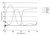
도 5는 컬러 필터 및 컬러 필터 적층체의 파장에 따른 투과율을 측정한 결과이다.
도 6은 본 발명의 일 실시예에 따른 표시 장치의 터치 영역을 나타낸 평면도이다.
도 7은 도 6에 도시된 터치 영역의 일부의 확대도이다.
도 8은 도 6에 도시된 터치 영역을 A-A 선을 따라 취한 단면도이다.
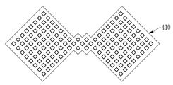
도 9는 각각 도 6에 도시한 터치 영역 중 제1 감지 전극의 부분 평면도이다.
도 10은 본 발명의 일 실시예에 따른 표시 장치의 표시 영역을 개략적으로 도시한 평면도이다.
도 11은 도 10의 XI-XI’선을 따라 잘라 도시한 단면도이다.
도 12 내지 도 15는 스페이서와 중첩하는 영역에서 컬러 필터 적층체를 형성하는 과정을 도시한 것이다.
도 16 내지 도 19는 스페이서가 위치하지 않는 영역에서 컬러 ??터를 형성하는 과정을 도시한 것이다.
도 20은 본 발명의 다른 일 실시예에 따른 표시 장치에 대하여 도 1과 동일한 단면을 도시한 것이다. 1 is a schematic cross-sectional view of a display device according to an exemplary embodiment of the present invention.
2 is a result of measuring the touch sensitivity (SNR) when the distance between the second electrode and the first sensing electrode is 8 µm, when there is no light blocking member (BM free) and when there is a light blocking member (BM + OCTA) to be.
3 is a result of measuring the touch sensitivity (SNR) when the distance between the second electrode and the first sensing electrode is 6 μm, when there is no light blocking member (BM free) and when there is a light blocking member (BM + OCTA) to be.
4 is a schematic plan view of a partial area in a display device according to an exemplary embodiment of the present invention.
5 is a result of measuring transmittance according to wavelength of a color filter and a color filter stack.
6 is a plan view illustrating a touch area of a display device according to an exemplary embodiment.
7 is an enlarged view of a part of the touch area illustrated in FIG. 6.
8 is a cross-sectional view of the touch area shown in FIG. 6 taken along line AA.
9 is a partial plan view of a first sensing electrode among the touch areas shown in FIG. 6, respectively.
10 is a plan view schematically illustrating a display area of a display device according to an exemplary embodiment.
11 is a cross-sectional view taken along line XI-XI' of FIG. 10.
12 to 15 illustrate a process of forming a color filter stack in a region overlapping the spacer.
16 to 19 illustrate a process of forming a color spacer in a region where a spacer is not located.
FIG. 20 is a cross-sectional view similar to that of FIG. 1 of a display device according to another exemplary embodiment of the present invention.
이하, 첨부한 도면을 참고로 하여 본 발명의 여러 실시예들에 대하여 본 발명이 속하는 기술 분야에서 통상의 지식을 가진 자가 용이하게 실시할 수 있도록 상세히 설명한다. 본 발명은 여러 가지 상이한 형태로 구현될 수 있으며 여기에서 설명하는 실시예들에 한정되지 않는다.Hereinafter, various embodiments of the present invention will be described in detail with reference to the accompanying drawings so that those of ordinary skill in the art may easily implement the present invention. The present invention may be implemented in various different forms and is not limited to the embodiments described herein.
본 발명을 명확하게 설명하기 위해서 설명과 관계없는 부분은 생략하였으며, 명세서 전체를 통하여 동일 또는 유사한 구성요소에 대해서는 동일한 참조 부호를 붙이도록 한다.In order to clearly describe the present invention, parts irrelevant to the description are omitted, and the same reference numerals are attached to the same or similar components throughout the specification.
또한, 도면에서 나타난 각 구성의 크기 및 두께는 설명의 편의를 위해 임의로 나타내었으므로, 본 발명이 반드시 도시된 바에 한정되지 않는다. 도면에서 여러 층 및 영역을 명확하게 표현하기 위하여 두께를 확대하여 나타내었다. 그리고 도면에서, 설명의 편의를 위해, 일부 층 및 영역의 두께를 과장되게 나타내었다.In addition, the size and thickness of each component shown in the drawings are arbitrarily shown for convenience of description, so the present invention is not necessarily limited to the illustrated bar. In the drawings, the thickness is enlarged in order to clearly express various layers and regions. And in the drawings, for convenience of description, the thickness of some layers and regions is exaggerated.
또한, 층, 막, 영역, 판 등의 부분이 다른 부분 "위에" 또는 "상에" 있다고 할 때, 이는 다른 부분 "바로 위에" 있는 경우뿐 아니라 그 중간에 또 다른 부분이 있는 경우도 포함한다. 반대로 어떤 부분이 다른 부분 "바로 위에" 있다고 할 때에는 중간에 다른 부분이 없는 것을 뜻한다. 또한, 기준이 되는 부분 "위에" 또는 "상에" 있다고 하는 것은 기준이 되는 부분의 위 또는 아래에 위치하는 것이고, 반드시 중력 반대 방향 쪽으로 "위에" 또는 "상에" 위치하는 것을 의미하는 것은 아니다.In addition, when a part such as a layer, film, region, plate, etc. is said to be "on" or "on" another part, this includes not only "directly over" another part, but also a case where another part is in the middle. . Conversely, when one part is "directly above" another part, it means that there is no other part in the middle. In addition, to be "above" or "on" the reference part means that it is located above or below the reference part, and does not necessarily mean that it is located "above" or "on" the direction opposite to gravity. .
또한, 명세서 전체에서, 어떤 부분이 어떤 구성요소를 "포함" 한다고 할 때, 이는 특별히 반대되는 기재가 없는 한 다른 구성요소를 제외하는 것이 아니라 다른 구성요소를 더 포함할 수 있는 것을 의미한다.In addition, throughout the specification, when a certain part "includes" a certain component, it means that other components may be further included rather than excluding other components unless otherwise stated.
또한, 명세서 전체에서, "평면상"이라 할 때, 이는 대상 부분을 위에서 보았을 때를 의미하며, "단면상"이라 할 때, 이는 대상 부분을 수직으로 자른 단면을 옆에서 보았을 때를 의미한다.In addition, throughout the specification, the term "on a plane" means when the object portion is viewed from above, and when the object portion is viewed from above, it means when the object portion is viewed from the side.
그러면 이하에서 본 발명의 일 실시예에 따른 표시 장치에 대하여 도면을 참고로 하여 상세하게 설명한다.Hereinafter, a display device according to an exemplary embodiment will be described in detail with reference to the drawings.
도 1은 본 발명의 일 실시예에 따른 표시 장치의 단면을 개략적으로 도시한 것이다. 도 1을 참고로 하면 본 발명의 일 실시예에 따른 표시 장치는 표시 영역(100), 터치 영역(400) 및 컬러 필터 영역(200)을 포함한다.1 is a schematic cross-sectional view of a display device according to an exemplary embodiment of the present invention. Referring to FIG. 1, a display device according to an embodiment of the present invention includes a
표시 영역(100)은 제1 기판(110) 및 제1 기판에 위치하는 트랜지스터(TFT)를 포함한다. 트랜지스터(TFT)는 절연막(180)에 위치하는 접촉 구멍을 통해 제1 전극(191)과 연결되어 있다. 격벽(361)의 개구부에는 발광 소자층(370)이 위치하고, 발광 소자층(370)을 사이에 두고 제1 전극(191)과 중첩하는 제2 전극(270)이 위치한다. The
격벽(361)의 일부는 위로 돌출되어 스페이서(362)를 구성한다. 스페이서(362)는 발광 소자층(370) 형성을 위해 마스크를 위치시키는 과정에서 격벽(361)의 손상을 방지한다. 스페이서(362)는 발광 소자층(370)의 유기 발광층 형성 공정에서 사용되는 마스크와 접촉한다. 즉 스페이서(362)는 격벽(361)과 마스크가 직접 접촉하는 것을 방지한다. 격벽(361)과 마스크가 직접 접촉하는 경우, 접촉 면적이 넓어서 마스크와 격벽(361)이 잘 분리되지 않고, 마스크 분리 과정에서 격벽(361)을 비롯한 각 층들이 박리되는 현상이 발생할 수 있다. 그러나 격벽(361) 중 일부에 스페이서(362)를 위치시키고 스페이서(362)와 마스크가 직접 접촉하도록 함으로써, 스페이서(362)와 마스크의 접촉 면적을 감소시키고 마스크를 용이하게 분리할 수 있다. A portion of the
스페이서(362)는 복수개의 격벽(361) 중 일부에만 위치한다. 일례로, 스페이서(362)는 10 개 내지 20 개의 격벽 중 하나 또는 둘 위에만 위치할 수 있다. 즉, 스페이서(362)의 배치 밀도는 5% 내지 20%일 수 있다. 본 발명에서 배치 밀도란 스페이서(362)가 위치하는 격벽의 수를 전체 격벽의 수로 나눈 값이다. The
스페이서(362)와 격벽(361) 개구부 가장자리 사이의 이격 거리는 5 ㎛ 내지 10 ㎛일 수 있다. 또한, 스페이서(362)의 가로, 세로 길이는 각각 10 ㎛ 내지 25 ㎛일 수 있다. 이 때의 이격 거리 및 가로, 세로 길이는 스페이서(362)의 하부를 기준으로 측정한 거리이다. 즉, 스페이서(362)의 하부면과 상부면의 면적이 다를 수 있으며, 본 명세서에서의 스페이서(362)의 가로, 세로 길이는 하부 면을 기준으로 측정한 것이다. 또한 스페이서(362)와 격벽(361) 개구부 가장자리 사이의 거리 또한 스페이서(362)의 하부면의 일 가장자리를 기준으로 측정한 것이다. A separation distance between the
스페이서(362)의 격벽으로부터의 높이는 1 ㎛ 내지 2 ㎛ 일 수 있다. 즉 격벽(361)과 스페이서(362)의 단차는 1 ㎛ 내지 2 ㎛ 일 수 있다. The height of the
도 1에서는 격벽(361)이 일부가 스페이서(362)인 구성을 도시하였다. 이 경우 격벽(361)과 스페이서(362)는 단일 공정으로 형성될 수 있으며 동일한 물질을 포함할 수 있다. 그러나 격벽(361)과 스페이서(362)를 각각 별도의 공정으로 형성하는 것 또한 가능하며, 이 경우 격벽(361)과 스페이서(362)는 서로 다른 물질을 포함할 수도 있다. In FIG. 1, a configuration in which a
제2 전극(270)은 격벽(361) 및 스페이서(362) 상에 위치한다. 제2 전극(270)에는 봉지부(390)가 위치한다. 봉지부(390)는 적어도 하나의 유기층 및 하나의 무기층을 포함할 수 있다.The
터치 영역(400)은 제1 절연층(431), 제1 감지 전극(410), 제2 감지 전극(미도시), 제2 절연층(432)을 포함한다. 제2 감지 전극은 도시되지 않았으나 제1 절연층(431) 상에 위치할 수 있다. 구체적인 터치 영역(400)의 구조는 후술한다. The
컬러 필터 영역(200)은 적색 컬러 필터(230R), 녹색 컬러 필터(230G) 및 청색 컬러 필터(230B)를 포함한다. 적색 컬러 필터(230R), 녹색 컬러 필터(230G) 및 청색 컬러 필터(230B)는 표시 장치의 저반사를 구현한다. 각 컬러 필터는 각각의 발광 소자층(370)과 중첩하여 위치한다. The
컬러 필터 영역(200)에는 차광 부재(220)가 위치한다. 차광 부재(220)는 격벽(361)과 중첩하여 위치할 수 있다. 차광 부재(220)를 사이에 두고 서로 다른 색의 컬러 필터가 위치할 수 있다. 다만 도 1을 참고로 하면, 스페이서(362)와 중첩하는 영역에는 차광 부재(220)가 아니라 컬러 필터 차광 부재 (221)가 위치한다. A
컬러 필터 차광 부재(221)는 적색 컬러 필터(230R), 녹색 컬러 필터(230G) 및 청색 컬러 필터(230B)가 적층되어 있으며, 차광 부재(220)와 유사하게 광을 흡수, 차단한다. The color filter
도 1을 참고로 하면, 표시 영역(100)의 스페이서(362)와 제1 기판(110)에 수직한 방향으로 중첩하는 영역에 차광 부재(220)가 위치하지 않고 컬러 필터 차광 부재(221)가 위치한다. 이로 인해, 터치 영역(400)의 감도 차이를 최소화 할 수 있다. 이하 효과에 대하여 상세하게 설명한다. Referring to FIG. 1, the
도 1을 참고로 하면, 격벽(361)에 위치하는 제2 전극(270)과 제1 감지 전극(410)사이의 간격(D1)과 스페이서(362)에 위치하는 제2 전극(270)과 제1 감지 전극(410) 사이의 간격(D2)이 상이하다. 스페이서(362)는 격벽(361)으로부터 돌출되어 있기 때문에 스페이서(362)에 위치하는 제2 전극(270)과 제1 감지 전극(410 사이의 간격(D2)이 격벽(361)에 위치하는 제2 전극(270)과 제1 감지 전극(410사이의 간격(D1)보다 좁다. Referring to FIG. 1, the gap D1 between the
일례로, 격벽(361)과 중첩하는 영역에서 제2 전극(270)과 제1 감지 전극(410) 사이의 거리(D1)는 8 ㎛ 내지 10 ㎛일 수 있다. 그러나 스페이서(362)와 중첩하는 영역에서 제2 전극(270)과 제1 감지 전극(410) 사이의 거리(D2)는 6㎛ 내지 8 ㎛일 수 있다. For example, a distance D1 between the
이렇게 제2 전극(270)과 제1 감지 전극(410)간의 간격이 상이한 경우, 터치 감도 차이가 발생한다. 제2 전극(270)과 제1 감지 전극(410) 사이의 유전층 두께에 따라 정전 용량이 달라지게 되고, 이러한 정전 용량은 터치 감도에 영향을 미친다. When the distance between the
제2 전극(270)과 제1 감지 전극(410)의 거리가 짧아질수록 제2 전극(270)에 의한 영향성이 커지며, 터치 감도가 감소하게 된다. 따라서 격벽(361)과 중첩하는 영역과 스페이서(362)와 중첩하는 영역에서의 터치 감도가 다르고 이는 터치 품질에 영향을 미친다. As the distance between the
그러나 본 실시예에 따른 표시 장치는 스페이서(362)와 중첩하는 영역의 차광 부재(220)를 제거하고 컬러 필터 차광 부재(221)가 차광 부재의 기능을 대신하게 함으로써, 영역별 터치 감도 차이를 최소화 하였다. However, in the display device according to the present exemplary embodiment, the difference in touch sensitivity for each region is minimized by removing the
차광 부재(220)는 광차단을 위하여 내부에 카본 블랙을 포함하고, 이러한 카본 블랙에 의하여 터치 감도가 감소하게 된다. 카본 블랙은 전도성을 가지기 때문에 터치 감도에 영향을 미친다. 그러나 본 실시예에 따른 표시 장치는 터치 감도가 감소하는 스페이서(362) 중첩 영역에 차광 부재(220)를 제거하였다. 따라서 스페이서(362) 중첩 영역에서 차광 부재(220)에 의한 터치 감도 감소가 발생하지 않으며, 격벽(361) 중첩 영역과 유사한 터치 감도를 가질 수 있다. The
도 2는 제2 전극(270)과 제1 감지 전극(410)의 거리가 8 ㎛일 때, 차광 부재가 없는 경우(BM Free)와 차광 부재가 존재하는 경우(BM + OCTA)의 터치 감도(SNR)를 측정한 결과이다. 도 3은 제2 전극(270)과 제1 감지 전극(410)의 거리가 6 ㎛일 때, 차광 부재가 없는 경우(BM free)와 차광 부재가 존재하는 경우(BM + OCTA)의 터치 감도(SNR)를 측정한 결과이다. 도 2 및 도 3에서, 각각의 조건에 대하여 4개의 표시 패널에 대하여 실험하였다. 2 shows the touch sensitivity (BM + OCTA) when the distance between the
도 2 및 도 3에 도시된 실시예 1 내지 16의 측정 조건 및 결과를 정리하면 하기 표 1과 같다.The measurement conditions and results of Examples 1 to 16 shown in FIGS. 2 and 3 are summarized in Table 1 below.
실시예 1 내지 4와 실시예 9 내지 12을 비교하면, 동일하게 차광 부재가 존재하지 않는 조건에서 제2 전극(270)과 제1 감지 전극(410)의 거리에 따라 터치 감도가 상이함을 확인할 수 있었다.Comparing Examples 1 to 4 with Examples 9 to 12, it was confirmed that the touch sensitivity was different according to the distance between the
즉 제2 전극(270)과 제1 감지 전극(410)의 거리가 8 ㎛인 경우가(실시예 1 내지 4), 거리가 6 ㎛인 경우(실시예 9 내지 12)에 비하여 터치 감도가 높음을 확인할 수 있었다. 평균치를 통해 비교해 보면, 차광 부재가 존재하지 않는 조건에서 거리가 8 ㎛일 때의 터치 감도가 24.1, 거리가 6 ㎛일 때의 터치 감도가 16.5로 나타났다.That is, when the distance between the
또한 실시예 1 내지 4와 실시예 5 내지 8을 비교하면, 제2 전극(270)과 제1 감지 전극(410)의 거리가 8 ㎛로 동일한 조건에서 차광 부재의 존재여부에 따라 터치 감도가 상이함을 확인할 수 있었다.In addition, when comparing Examples 1 to 4 and Examples 5 to 8, the distance between the
즉 차광 부재가 존재하지 않는 경우(실시예 1 내지 4)가, 차광 부재가 존재하는 경우(실시예 5 내지 8)에 비하여 터치 감도가 높게 나타났다. 평균치를 통해 비교해보면, 거리가 동일한 조건에서 차광 부재가 존재하지 않는 경우의 터치 감도 평균은 24.1 이고, 차광 부재가 존재하는 경우의 터치 감도 평균은 16.5 이었다.That is, the case where the light blocking member does not exist (Examples 1 to 4) showed higher touch sensitivity than the case where the light blocking member was present (Examples 5 to 8). Comparing through the average value, the average of the touch sensitivity when the light blocking member was not present under the same distance was 24.1, and the average of the touch sensitivity when the light blocking member was present was 16.5.
마찬가지로, 실시예 9 내지 12와 실시예 13 내지 16을 비교하면, 제2 전극(270)과 제1 감지 전극(410)의 거리가 6 ㎛로 동일한 조건에서 차광 부재가 존재여부에 따라 터치 감도가 상이함을 확인할 수 있었다.Similarly, when comparing Examples 9 to 12 and Examples 13 to 16, the distance between the
즉 차광 부재가 존재하지 않는 경우(실시예 9 내지 12)가, 차광 부재가 존재하는 경우(실시예 13 내지 16)에 비하여 터치 감도가 높게 나타났다. 평균치를 통해 비교해보면, 차광 부재가 존재하지 않는 경우의 터치 감도 평균은 16.5 이고, 차광 부재가 존재하는 경우의 터치 감도 평균은 11.9 이었다.That is, the case where the light blocking member does not exist (Examples 9 to 12) has a higher touch sensitivity than the case where the light blocking member is present (Examples 13 to 16). Comparing through the average value, the average of the touch sensitivity when the light blocking member was not present was 16.5, and the average of the touch sensitivity when the light blocking member was present was 11.9.
상기 표 1, 도 2 및 도 3을 통해 확인할 수 있는 바와 같이 터치 감도는 제2 전극(270)과 제1 감지 전극(410)의 거리가 길어질수록 증가하고, 차광 부재가 존재하는 경우보다 존재하지 않는 경우에 더 높게 나타났다.As can be seen from Tables 1, 2, and 3, the touch sensitivity increases as the distance between the
상기 표 1에서, 제2 전극(270)과 제1 감지 전극(410)의 거리가 8 ㎛ 이고 차광 부재가 존재하는 실시예 5 내지 8의 터치 감도 평균값은 16.5로 나타났다. 또한, 제2 전극(270)과 제1 감지 전극(410)의 거리가 6 ㎛ 이고 차광 부재가 존재하지 않는 실시예 9 내지 12의 터치 감도 평균값은 16.5로 나타났다. 즉, 실시예 9 내지 12는 실시예 5 내지 8에 비하여 제2 전극(270)과 제1 감지 전극(410) 사이의 거리가 짧지만, 차광 부재가 존재하지 않기 때문에 실시예 5 내지 8과 유사한 터치 감도를 가지는 것을 확인할 수 있었다.In Table 1, the average value of the touch sensitivity of Examples 5 to 8 in which the distance between the
본 발명 실시예에서, 실시예 5 내지 8의 결과는 격벽(361)과 중첩하는 영역에서의 터치 감도에 대응하고, 실시예 9 내지 12의 결과는 스페이서(362)와 중첩하는 영역에서의 터치 감도에 대응한다. In the embodiment of the present invention, the results of Examples 5 to 8 correspond to the touch sensitivity in the area overlapping the
상기 결과를 통해 확인할 수 있는 바와 같이 본 발명의 일 실시예에 따른 표시 장치에서, 스페이서(362)와 중첩하는 영역의 차광 부재(220)를 제거함으로써 스페이서(362) 중첩 영역과 격벽(361) 중첩 영역의 거리 차이에 의한 터치 감도 차이를 최소화하였다. As can be seen from the above results, in the display device according to the exemplary embodiment of the present invention, the
본 실시예에 따른 표시 장치는 내부에 편광층을 포함하지 않는다. 본 실시예에 따른 표시 장치는 컬러 필터 영역(200)을 포함하기 때문에 이로 인해 휘도가 일부 감소하였으며, 편광층을 포함하는 경우 휘도가 지나치게 감소하는바 바람직하지 않다. The display device according to the present exemplary embodiment does not include a polarizing layer therein. Since the display device according to the present exemplary embodiment includes the
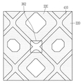
도 4는 본 발명의 일 실시예에 따른 표시 장치에서 일부 영역의 평면도를 간략하게 도시한 것이다. 도 4를 참고로 하면 스페이서(362)는 컬러 필터(230B, 230G, 230R) 사이에 위치하며, 제1 감지 전극(410)과 중첩한다. 이렇게 제1 감지 전극(410)과 스페이서(362)가 중첩하는 영역에서 제1 감지 전극(410)과 제2 전극(미도시)의 거리가, 미중첩 영역과 비교하여 짧아지기 때문에 터치 감도가 달라진다. 본 발명은 이를 해결하기 위하여 스페이서(362) 중첩 영역의 차광 부재(220)를 제거한 것을 특징으로 한다. 도 1은 도 4에서 I-I'으로 잘라 도시한 단면과 유사하게 대응할 수 있다. 4 is a schematic plan view of a partial area in a display device according to an exemplary embodiment of the present invention. Referring to FIG. 4, the
이렇게 차광 부재(220)가 제거된 영역은 컬러 필터 차광 부재(221)가 위치하여 광을 차단한다. 도 4에서는 컬러 필터(230R, 230G, 230B)가 차광 부재(220)와 중첩하지 않는 구성으로 도시되었으나 실제로 컬러 필터(230R, 230G, 230B)의 가장자리와 차광 부재(220)는 일부 중첩할 수 있다.In the area from which the
도 5는 각 컬러 필터 및 컬러 필터 차광 부재의 파장에 따른 투과율을 측정한 결과이다. 도 5를 참고로 하면 컬러 필터 차광 부재(R/G/B)는 가시광선 파장 영역에서 낮은 투과율을 나타냄을 확인할 수 있었다. 따라서, 차광 부재(220)가 제거되더라도 컬러 필터 차광 부재(R/G/B)가 광차단 기능을 수행할 수 있음을 확인할 수 있었다. 5 is a result of measuring transmittance according to wavelength of each color filter and a color filter light blocking member. Referring to FIG. 5, it was confirmed that the color filter light blocking member (R/G/B) exhibited low transmittance in the visible light wavelength region. Accordingly, it was confirmed that even if the
그러면 이하에서, 본 발명의 일 실시예에 따른 표시 장치에서 터치 영역(400) 및 표시 영역(100)의 구체적인 구조 및 관계에 대하여 도면을 참고로 하여 상세하게 설명한다. Hereinafter, a detailed structure and relationship between the
도 6은 본 발명의 일 실시예에 따른 표시 장치의 터치 영역의 일부를 나타낸 평면도이고, 도 7은 도 6에 도시된 터치 영역의 일부의 확대도이고, 도 8은 도 6에 도시된 터치 영역을 A-A 선을 따라 취한 단면도이다. 도 9는 도 6에 도시한 제1 감지 전극의 부분 평면도이다.6 is a plan view illustrating a part of a touch area of a display device according to an exemplary embodiment, FIG. 7 is an enlarged view of a part of the touch area shown in FIG. 6, and FIG. 8 is a touch area shown in FIG. 6. Is a cross-sectional view taken along line AA. 9 is a partial plan view of the first sensing electrode shown in FIG. 6.
터치 영역의 터치 센서는 다양한 방식으로 접촉을 감지할 수 있다. 터치 센서는 저항막 방식(resistive type), 정전용량 방식(capacitive type), 전자기 유도 방식(electro-magnetic type), 광 감지 방식(optical type) 등의 방식으로 분류될 수 있다. 여기서는 정전용량 방식의 터치 센서를 예로 들어 설명한다.The touch sensor of the touch area can detect a touch in various ways. Touch sensors may be classified into a resistive type, a capacitive type, an electro-magnetic type, and an optical type. Here, a capacitive touch sensor will be described as an example.
도 6을 참조하면, 터치 영역은 복수의 감지 전극(410, 420)을 포함한다. 복수의 감지 전극은 복수의 제1 감지 전극(410) 및 복수의 제2 감지 전극(420)을 포함할 수 있다. 제1 감지 전극(410)과 제2 감지 전극(420)은 서로 분리되어 있다.Referring to FIG. 6, the touch area includes a plurality of
복수의 제1 감지 전극(410) 및 복수의 제2 감지 전극(420)은 터치 영역(TA)에서 서로 중첩되지 않도록 교호적으로 분산되어 배치될 수 있다. 복수의 제1 감지 전극(410)은 열 방향 및 행 방향을 따라 각각 복수 개씩 배치되고, 복수의 제2 감지 전극(420)도 열 방향 및 행 방향을 따라 각각 복수 개씩 배치될 수 있다.The plurality of
제1 감지 전극(410)과 제2 감지 전극(420)은 서로 동일한 층에 위치하지만, 서로 다른 층에 위치할 수도 있다. 제1 감지 전극(410)과 제2 감지 전극(420) 대체로 사각형일 수 있으나, 이에 한정되는 것은 아니고, 육각형 등의 다각형이나 원형, 타원형일 수 있고, 터치 센서의 감도 향상을 위해 돌출부를 가지는 등 다양한 형태를 가질 수 있다. 또한, 각각의 제1 감지 전극(410) 및 제2 감지 전극(420)은 도 9에 도시된 바와 같이 메쉬 형태일 수 있다. The
동일한 행 또는 열에 배열된 복수의 제1 감지 전극(410)의 적어도 일부는 터치 영역(TA) 내부 또는 외부에서 서로 연결되어 있을 수도 있고 분리되어 있을 수도 있다. 마찬가지로, 동일한 열 또는 행에 배열된 복수의 제2 감지 전극(420)의 적어도 일부는 터치 영역(TA) 내부 또는 외부에서 서로 연결되어 있을 수도 있고 분리되어 있을 수도 있다. 예컨대, 도 6에 도시된 바와 같이, 동일한 행에 배치된 복수의 제1 감지 전극(410)이 터치 영역(TA) 내부에서 서로 연결되어 있는 경우, 동일한 열에 배치된 복수의 제2 감지 전극(420)이 터치 영역(TA) 내부에서 서로 연결되어 있을 수 있다. 즉, 각 행에 위치하는 복수의 제1 감지 전극(410)은 제1 연결부(connector)(412)를 통해 서로 연결되어 있고, 각 열에 위치하는 복수의 각 열에 위치하는 복수의 제2 감지 전극(420)은 제2 연결부(422)를 통해 서로 연결되어 있을 수 있다.At least some of the plurality of
도 7 및 도 8을 참조하면, 서로 이웃하는 제2 감지 전극(420) 사이를 연결하는 제2 연결부(422)가 표시 영역(100)위에 위치하고, 그 위에 제1 절연층(431)이 위치한다. 제1 절연층(431) 위에는 제1 감지 전극(410), 제2 감지 전극(420), 그리고 서로 이웃하는 제1 감지 전극(410) 사이를 연결하는 제1 연결부(412)가 위치한다. 제1 감지 전극(410) 제2 감지 전극(420) 및 제1 연결부(412) 위에는 이들을 보호하기 위한 제2 절연층(432)이 위치한다. Referring to FIGS. 7 and 8, a
제2 감지 전극(420)은 제1 절연층(431)에 형성되어 있는 접촉 구멍을 통해 제2 연결부(422)와 전기적으로 연결된다. 제1 연결부(412)의 일부는 제2 연결부(422)와 중첩하지만, 제1 절연층(431)에 의해 물리적으로 및 전기적으로 분리되어 있다. 제1 감지 전극(410), 제2 감지 전극(420) 및 제1 연결부(412)는 동일한 물질로 형성될 수 있고, 동시에 패터닝될 수 있다. 제2 연결부(422)는 터치 신호선(411, 421)과 동일한 물질로 형성될 수 있고, 동시에 패터닝될 수 있다.The
한편, 제2 감지 전극(420)과 제1 연결부(412)가 상부 기판(210) 위에 동일한 층에 위치하고 제1 절연층(431)을 사이에 두고 제2 감지 전극(420) 및 제1 연결부(412) 위로 제2 연결부(422)가 형성될 수도 있다. 다른 한편, 서로 이웃하는 제2 감지 전극(420) 사이를 연결하는 제2 연결부(422)가 제1 감지 전극(410)과 동일한 층에 위치하며 제2 감지 전극(420)과 일체화되어 있고, 서로 이웃하는 제1 감지 전극(410) 사이를 연결하는 제1 연결부(412)는 제1 감지 전극(410)과 다른 층에 위치할 수도 있다. 그 밖에도 감지 전극 간의 연결을 위한 다양한 변형 예가 존재한다.Meanwhile, the
다시 도 6을 참조하면, 각 행의 서로 연결된 제1 감지 전극(410)은 제1 터치 신호선(411)을 통해 터치 센서 제어부(도시되지 않음)와 연결되고, 각 열의 서로 연결된 제2 감지 전극(420)은 제2 터치 신호선(421)을 통해 터치 센서 제어부와 연결될 수 있다. 제1 터치 신호선(411)과 제2 터치 신호선(421)은 도시된 바와 같이 표시 패널의 주변 영역(PA)에 위치하지만, 이와 달리 터치 영역(TA)에 위치할 수도 있다.Referring back to FIG. 6, the
제1 감지 전극(410) 및 제2 감지 전극(420)은 표시 영역(100)으로부터 빛이 투과될 수 있도록 소정의 투과도 이상을 가질 수 있다. 예를 들어 제1 감지 전극(410) 및 제2 감지 전극(420)은 인듐 주석 산화물(ITO), 인듐 아연 산화물(IZO), 은 나노 와이어(AgNW) 등의 얇은 금속층, 메탈 메쉬(metal mesh), 탄소 나노 튜브(CNT) 등의 투명한 도전 물질로 만들어질 수 있으나 이에 한정되는 것은 아니다.The
서로 이웃하는 제1 감지 전극(410)과 제2 감지 전극(420)은 터치 센서로서 기능하는 상호 축전기(mutual capacitor)를 형성한다. 상호 축전기는 제1 감지 전극(410)과 제2 감지 전극(420) 중 하나를 통해 구동 신호를 입력받고 외부 물체의 터치에 의한 전하량 변화를 감지 신호로서 나머지 감지 전극을 통해 출력할 수 있다.The
도 6 내지 도 8에 도시된 것과 달리, 복수의 제1 감지 전극(410)이 서로 분리되고 복수의 제2 감지 전극(420)도 서로 분리되어 독립적인 감지 전극을 형성하고 각자의 터치 배선(도시되지 않음)을 통해 터치 센서 제어부와 연결될 수도 있다. 이 경우 각 감지 전극은 터치 센서로서 자기 축전기(self-capacitor)를 형성할 수 있다. 자기 축전기는 구동 신호를 입력받아 소정 전하량으로 충전될 수 있고, 손가락 등의 외부 물체의 접촉이 있으면 충전 전하량에 변화가 생겨 입력된 구동 신호와 다른 감지 신호를 출력할 수 있다.6 to 8, a plurality of
도 9를 참고로 하면 제1 감지 전극(410)은 그물(mesh) 모양으로 형성될 수 있다. 별도의 도면으로 도시하지는 않았으나, 제2 감지 전극(420) 또한 그물 모양일 수 있다. 각각의 그물 형상의 감지 전극(410, 420)은 격벽(361)과 중첩하여 위치할 수 있다. Referring to FIG. 9, the
그럼 이하에서 도 10 및 도 11을 참고로 하여 본 발명의 일 실시예에 따른 표시 장치의 표시 영역(100)의 구체적인 구조에 대하여 설명한다.Then, a detailed structure of the
도 10은 본 발명의 일 실시예에 따른 표시 장치의 표시 영역을 개략적으로 도시한 평면도이다. 도 11은 도 10의 XI-XI’선을 따라 잘라 도시한 단면도이다.10 is a plan view schematically illustrating a display area of a display device according to an exemplary embodiment. 11 is a cross-sectional view taken along line XI-XI' of FIG. 10.
도면에서는 표시 영역의 각 화소에 두 개의 박막 트랜지스터(thin film transistor, TFT)(T1, T2)와 하나의 축전 소자(C1)를 구비하는 2Tr-1Cap 구조의 능동 구동(activematrix, AM)형 발광 표시 장치를 도시하고 있으나, 본 발명 및 본 실시예가 이에 한정되는 것은 아니다.In the drawing, an active matrix (AM) type light-emitting display having a 2Tr-1Cap structure including two thin film transistors (TFTs) (T1, T2) and one power storage element (C1) in each pixel of the display area Although an apparatus is shown, the present invention and the present embodiment are not limited thereto.
따라서 발광 표시 장치는 하나의 화소에 셋 이상의 트랜지스터와 둘 이상의 축전 소자를 구비할 수 있으며, 별도의 배선이 더 형성되어 다양한 구조를 가질 수 있다. 여기서, 화소는 화상을 표시하는 최소 단위를 말하며, 표시 영역은 복수의 화소들을 통해 화상을 표시한다.Accordingly, the light emitting display device may include three or more transistors and two or more power storage elements in one pixel, and separate wirings may be further formed to have various structures. Here, a pixel refers to a minimum unit for displaying an image, and the display area displays an image through a plurality of pixels.
도 10 및 도 11을 참조하면, 본 실시예에 따른 발광 표시 장치는 기판(110)에 위치하는 복수의 화소 각각에 형성된 스위칭 박막 트랜지스터(T1), 구동 박막 트랜지스터(T2), 축전 소자(C1), 그리고 발광 소자(E1)를 포함한다. 기판(110)에는 일 방향을 따라 배치되는 게이트선(121)과, 게이트선(121)과 절연 교차되는 데이터선(171) 및 공통 전원선(172)이 위치한다. 여기서, 각 화소는 게이트선(121), 데이터선(171) 및 공통 전원선(172)을 경계로 정의될 수 있으나, 반드시 이에 한정되는 것은 아니다. Referring to FIGS. 10 and 11, in the light emitting display device according to the present exemplary embodiment, a switching thin film transistor T1, a driving thin film transistor T2, and a power storage element C1 formed in each of a plurality of pixels positioned on a
유기 발광 소자(E1)는, 제1 전극(191)과, 제1 전극(191) 상에 형성된 발광 소자층(370)과, 이 발광 소자층(370) 상에 형성된 제2 전극(270)을 포함한다. The organic light emitting device E1 includes a
여기서 제1 전극(191)이 정공 주입 전극인 양극이며, 제2 전극(270)이 전자 주입 전극인 음극이 된다. 그러나 본 발명이 이에 한정되는 것은 아니며, 발광 표시 장치의 구동 방법에 따라 제1 전극(191)이 음극이 되고, 제2 전극(270)이 양극이 될 수도 있다. 제1 전극(191)은 화소 전극일 수 있고, 제2 전극(270)은 공통 전극일 수 있다. Here, the
발광 소자층(370)은 정공 주입층, 정공 수송층, 발광층, 전자 수송층, 전자 주입층 중 하나 이상을 포함할 수 있다. 이 중 발광층은 유기 발광층을 포함할 수 있으며, 주입된 정공과 전자가 결합하여 생성된 엑시톤(exciton)이 여기 상태로부터 기저 상태로 떨어질 때 발광이 이루어진다. 또는 발광층은 양자점을 포함할 수도 있다. The light emitting
축전 소자(C1)는 층간 절연막(160)을 사이에 두고 배치된 한 쌍의 축전판(158, 178)을 포함한다. 여기서, 층간 절연막(160)은 유전체가 된다. 축전 소자(C1)에 축적된 전하와 한 쌍의 축전판(158, 178) 사이의 전압에 의해 축전 용량이 결정된다.The power storage element C1 includes a pair of
스위칭 박막 트랜지스터(T1)는, 스위칭 반도체층(151), 스위칭 게이트 전극(122), 스위칭 소스 전극(176), 및 스위칭 드레인 전극(177)을 포함한다. 구동 박막 트랜지스터(T2)는 구동 반도체층(155), 구동 게이트 전극(124), 구동 소스 전극(173) 및 구동 드레인 전극(175)을 포함한다.The switching thin film transistor T1 includes a switching
스위칭 박막 트랜지스터(T1)는 발광시키고자 하는 화소를 선택하는 스위칭 소자로 사용된다. 스위칭 게이트 전극(122)은 게이트선(121)에 연결되고, 스위칭 소스 전극(176)은 데이터선(171)에 연결된다. 스위칭 드레인 전극(177)은 스위칭 소스 전극(176)으로부터 이격 배치되며 어느 한 축전판(158)과 연결된다. The switching thin film transistor T1 is used as a switching element for selecting a pixel to emit light. The switching gate electrode 122 is connected to the
구동 박막 트랜지스터(T2)는 선택된 화소 내의 유기 발광 소자(E1)의 발광 소자층(370)을 발광시키기 위한 구동 전원을 제1 전극(191)에 인가한다. 구동 게이트 전극(124)은 스위칭 드레인 전극(177)과 연결된 축전판(158)에 연결된다. 구동 소스 전극(173) 및 다른 한 축전판(178)은 각각 공통 전원선(172)에 연결된다.The driving thin film transistor T2 applies driving power to the
구동 드레인 전극(175)이 접촉 구멍(185)을 통해 제1 전극(191)에 연결된다.The driving
도 10과 함께 도 11을 참조하여, 본 발명의 일 실시예에 따른 유기 발광 표시 장치를 좀더 상세하게 설명하면 다음과 같다. Referring to FIG. 11 along with FIG. 10, an organic light emitting display device according to an exemplary embodiment of the present invention will be described in more detail as follows.
제1 기판(110)위에 버퍼층(111)이 위치한다. 제1 기판(110)은 유리, 석영, 세라믹, 플라스틱 등으로 이루어질 수 있다. 버퍼층(111)은 실리콘 나이트라이드(SiNx), 실리콘옥사이드(SiO2), 실리콘옥시나이트라이드(SiOxNy) 등으로 이루어질 수 있으나 이에 제한되는 것은 아니다. 상기 x,y는 각각 1 내지 5일 수 있다. A
버퍼층(111) 위에 구동 반도체층(155)이 형성된다. 구동 반도체층(155)은 다결정 실리콘막, 비정질 실리콘막 등의 다양한 반도체 물질로 이루어질 수 있다. 구동 반도체층(155)은 소스 영역(152), 채널 영역(153) 및 드레인 영역(154)을 포함할 수 있다. A driving
구동 반도체층(155) 위에 실리콘나이트라이드 또는 실리콘옥사이드 등으로 이루어진 게이트 절연막(140)이 위치한다. 게이트 절연막(140) 위에 구동 게이트 전극(124) 및 제1 축전판(158)이 위치한다. 이때, 구동 게이트 전극(124)은 구동 반도체층(155)의 적어도 일부, 구체적으로 채널 영역(153)과 중첩하여 위치한다.A
게이트 절연막(140) 상에는 구동 게이트 전극(124)을 덮는 층간 절연막 (160)이 위치한다. 층간 절연막(160)은 게이트 절연막(140)과 마찬가지로 실리콘나이트라이드 또는 실리콘옥사이드 등으로 형성될 수 있다. 게이트 절연막(140)과 층간 절연막(160)은 구동 반도체층(155)의 소스 영역(152) 및 드레인 영역(154)을 드러내는 제1 접촉 구멍(163) 및 제2 접촉 구멍(165)을 갖는다.An interlayer insulating
층간 절연막 (160) 위에 구동 소스 전극(173) 및 구동 드레인 전극(175), 데이터선(171), 공통 전원선(172), 제2 축전판(178)이 위치한다. 구동 소스 전극(173) 및 구동 드레인 전극(175)은 각각 제1 접촉 구멍(163) 및 제2 접촉 구멍(165)을 통해 구동 반도체층(155)의 소스 영역(152) 및 드레인 영역(154)과 연결된다. A driving
층간 절연막(160) 상에는 구동 소스 전극(173), 구동 드레인 전극(175)을 덮는 절연막(180)이 위치한다. 절연막(180)은 폴리아크릴계, 폴리이미드계 등과 같은 유기물을 포함할 수 있다.An insulating
절연막(180)은 접촉 구멍(185)을 갖는다. 제1 전극(191)은 절연막 (180)상에 위치한다. 제1 전극(191)은 화소 전극일 수 있다. 제1 전극(191)은 접촉 구멍(185)을 통하여 구동 드레인 전극(175)과 연결되어 있다. The insulating
격벽(361)은 절연막(180) 상에 위치한다. 격벽(361)의 일부는 돌출되어 스페이서(미도시)를 구성할 수 있다. 격벽(361)은 개구부를 포함하고, 상기 개구부에 제1 전극(191)과 중첩하여 발광 소자층(370)이 위치하고, 발광 소자층(370)과 중첩하도록 제2 전극(270)이 위치한다. 발광 소자층(370)은 정공 주입층, 정공 수송층, 발광층, 전자 수송층, 전자 주입층 중 하나 이상을 포함할 수 있다. 제2 전극(270)은 공통 전극일 수 있다. 발광 소자(E1)는 제1 전극(191), 발광 소자층(370) 및 제2 전극(270)을 포함한다.The
그러면 이하에서 도 12 내지 19를 참고로 하여 본 발명의 일 실시예에 따른 표시 장치에서 컬러 필터 차광 부재(221)를 형성하는 공정에 대하여 설명한다. 도 12 내지 도 15는 스페이서(362)와 중첩하는 영역에서 컬러 필터 차광 부재(221)를 형성하는 과정을 도시한 것이고, 도 16 내지 도 19는 스페이서(362)가 위치하지 않는 영역에서 컬러 ??터를 형성하는 과정을 도시한 것이다. Hereinafter, a process of forming the color filter
도 12 및 도 16을 참고로 하면, 컬러 필터가 형성되지 않은 표시 장치가 위치한다. 도 12에 도시된 영역은 스페이서(362)가 위치하고, 도 16에 도시된 영역은 스페이서가 위치하지 않는 영역이다.12 and 16, a display device on which a color filter is not formed is positioned. The area shown in FIG. 12 is an area where the
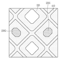
다음 도 13 및 도 17을 참고로 하면, 녹색 컬러 필터(230G)를 형성한다. 도 17을 참고로 하면 스페이서(362)가 위치하지 않는 영역에서 녹색 컬러 필터(230G)는 제1 감지 전극(410)과 중첩하지 않고 형성되지만, 도 13을 참고로 하면 스페이서(362)가 위치하는 영역에서 녹색 컬러 필터(230G)는 제1 감지 전극(410) 및 스페이서(362)와 중첩하여 형성된다.Next, referring to FIGS. 13 and 17, a
다음 도 14 및 도 18을 참고로 하면 적색 컬러 필터(230R)를 형성한다. 도 18을 참고로 하면 스페이서(362)가 위치하지 않는 영역에서, 적색 컬러 필터(230R)는 녹색 컬러 필터(230G) 및 제1 감지 전극(410)과 중첩하지 ?方? 형성된다. 그러나 도 14를 참고로 하면, 스페이서(362)가 위치하는 영역에서 적색 컬러 필터(230R)는 스페이서(362)와 중첩하여 형성된다. 따라서 스페이서(362) 상부에는 도 13에서 형성된 녹색 컬러 필터(230G) 및 도 14에서 형성된 적색 컬러 필터(230R)가 중첩하여 위치한다.Next, referring to FIGS. 14 and 18, a
다음, 도 15 및 도 19를 참고로 하면 청색 컬러 필터(230B)를 형성한다. 도 19을 참고로 하면, 스페이서(362)가 위치하지 않는 영역에서, 청색 컬러 필터(230B)는 적색 컬러 필터(230R), 녹색 컬러 필터(230G) 및 제1 감지 전극(410)과 중첩하지 않고 형성된다. 그러나 도 15를 참고로 하면 스페이서(362)가 위치하는 영역에서 청색 컬러 필터(230B)는 스페이서(362)와 중첩하여 형성된다. 따라서 스페이서(362) 상부에는 도 13에서 형성된 녹색 컬러 필터(230G), 도 14에서 형성된 적색 컬리 ?i러(230R) 및 도 15에서 형성된 청색 컬러 필터(230B)가 중첩하여 위치한다.Next, referring to FIGS. 15 and 19, a
도 13 내지 도 19에서 컬러 필터(230R, 230G, 230B)가 차광 부재(220)와 중첩하지 않는 구성으로 도시되었으나 실제로 컬러 필터(230R, 230G, 230B)의 가장자리와 차광 부재(220)는 일부 중첩할 수 있다.13 to 19, the
도 20은 본 발명의 다른 일 실시예에 따른 표시 장치에 대하여 도 1과 동일한 단면을 도시한 것이다. 도 20을 참고로 하면 본 실시예에 따른 표시 장치는 컬러 필터 차광 부재(221)가 적색 컬러 필터(230R) 및 청색 컬러 필터(230B)만을 포함한다는 점을 제외하고는 도 1의 실시예에 따른 표시 장치와 동일하다. 동일한 구성요소에 대한 구체적인 설명은 생략한다. 도 20을 참고로 하면, 컬러 필터 차광 부재(221)가 녹색 컬러 필터를 포함하지 않고 적색 컬러 필터(230R) 및 청색 컬러 필터(230B)만을 포함하는 경우에도 도 1에서와 유사하게 광을 차단할 수 있다. FIG. 20 is a cross-sectional view similar to that of FIG. 1 of a display device according to another exemplary embodiment of the present invention. Referring to FIG. 20, the display device according to the present exemplary embodiment is according to the exemplary embodiment of FIG. 1 except that the color filter
이상과 같이 본 발명의 일 실시예에 따른 표시 장치는 스페이서(362)와 중첩하는 영역의 차광 부재(220)를 제거하고 컬러 필터 차광 부재(221)가 차광 부재의 기능을 대신하게 함으로써, 스페이서(362)가 위치하는 영역과 격벽(361)이 위치하는 영역에서의 제2 전극(270)과 제1 감지 전극(410) 사이의 거리 차이에 의한 터치 감도 차이를 최소화 하였다. As described above, in the display device according to an exemplary embodiment, by removing the
이상에서 본 발명의 실시예에 대하여 상세하게 설명하였지만 본 발명의 권리범위는 이에 한정되는 것은 아니고 다음의 청구범위에서 정의하고 있는 본 발명의 기본 개념을 이용한 당업자의 여러 변형 및 개량 형태 또한 본 발명의 권리범위에 속하는 것이다.Although the embodiments of the present invention have been described in detail above, the scope of the present invention is not limited thereto, and various modifications and improvements by those skilled in the art using the basic concept of the present invention defined in the following claims are also provided. It belongs to the scope of rights.
100: 표시 영역
200: 컬러 필터 영역
400: 터치 영역
110: 제1 기판
191: 제1 전극
270: 제2 전극
361: 격벽
362: 스페이서
410: 제1 감지 전극
420: 제2 감지 전극
370: 발광 소자층
390: 봉지부
.100: display area 200: color filter area
400: touch area 110: first substrate
191: first electrode 270: second electrode
361: bulkhead 362: spacer
410: first sensing electrode 420: second sensing electrode
370: light emitting element layer 390: sealing portion
.
Claims (23)
상기 표시 영역과 중첩하여 위치하는 컬러 필터 영역;
상기 표시 영역과 상기 컬러 필터 영역 사이에 위치하는 터치 영역을 포함하고,
상기 표시 영역은
복수개의 트랜지스터가 위치하는 제1 기판;
상기 트랜지스터와 연결된 제1 전극;
상기 제1 전극 상에 위치하며, 상기 제1 전극과 중첩하는 개구부를 갖는 격벽;
상기 격벽 상에 위치하는 제2 전극;
상기 제1 전극과 상기 제2 전극 사이에 위치하는 발광층;
상기 복수개의 격벽 중 일부 격벽에 위치하는 스페이서를 포함하고,
상기 컬러 필터 영역은
복수개의 차광 부재 및 컬러 필터 차광 부재;
상기 차광 부재와 상기 컬러 필터 차광 부재 사이에 위치하는 컬러 필터를 포함하고,
상기 스페이서와 상기 컬러 필터 차광 부재는 상기 제1 기판에 수직한 방향으로 중첩하는 표시 장치. Display area;
A color filter area overlapping the display area;
And a touch area positioned between the display area and the color filter area,
The display area is
A first substrate on which a plurality of transistors are located;
A first electrode connected to the transistor;
A partition wall positioned on the first electrode and having an opening overlapping the first electrode;
A second electrode positioned on the partition wall;
A light-emitting layer positioned between the first electrode and the second electrode;
And a spacer positioned on some of the plurality of partitions,
The color filter area is
A plurality of light blocking members and color filter light blocking members;
A color filter positioned between the light blocking member and the color filter light blocking member,
The spacer and the color filter light blocking member overlap the first substrate in a direction perpendicular to the display device.
상기 스페이서와 상기 차광 부재는 상기 제1 기판에 수직한 방향으로 서로 중첩하지 않는 표시 장치. In claim 1,
The spacer and the light blocking member do not overlap each other in a direction perpendicular to the first substrate.
상기 컬러 필터 차광 부재는 적색 컬러 필터, 녹색 컬러 필터 및 청색 컬러 필터의 일부가 적층된 적층체인 표시 장치. In claim 1,
The color filter light blocking member is a display device in which a red color filter, a green color filter, and a blue color filter are partially stacked.
상기 터치 영역은 제1 감지 전극 및 제2 감지 전극을 포함하고,
상기 제1 감지 전극 및 상기 제2 감지 전극은 상기 차광 부재와 중첩하여 위치하는 표시 장치. In claim 1,
The touch area includes a first sensing electrode and a second sensing electrode,
The first sensing electrode and the second sensing electrode are positioned to overlap the light blocking member.
상기 스페이서와 중첩하는 영역에서 상기 제2 전극과 상기 제1 감지 전극 사이의 거리는 8 ㎛ 내지 10 ㎛인 표시 장치. In claim 4,
A distance between the second electrode and the first sensing electrode in a region overlapping the spacer is 8 µm to 10 µm.
상기 격벽과 중첩하는 영역에서 상기 제2 전극과 상기 제1 감지 전극 사이의 거리는 6 ㎛ 내지 8 ㎛인 표시 장치. In claim 4,
A display device having a distance between the second electrode and the first sensing electrode in an area overlapping the partition wall is 6 µm to 8 µm.
상기 제1 감지 전극 및 상기 제2 감지 전극은 메쉬 구조이며,
상기 제1 감지 전극 및 상기 제2 감지 전극은 상기 차광 부재와 중첩하여 위치하는 표시 장치. In claim 4,
The first sensing electrode and the second sensing electrode have a mesh structure,
The first sensing electrode and the second sensing electrode are positioned to overlap the light blocking member.
상기 제1 감지 전극 및 상기 제2 감지 전극은 상기 발광 소자층과 중첩하지 않는 표시 장치.In clause 7,
The first sensing electrode and the second sensing electrode do not overlap the light emitting element layer.
상기 격벽과 상기 스페이서의 높이 차이는 1 ㎛ 내지 2 ㎛ 인 표시 장치.In claim 1,
The height difference between the partition wall and the spacer is 1 µm to 2 µm.
상기 컬러 필터 차광 부재는 상기 녹색 컬러 필터, 상기 적색 컬러 필터 및 상기 청색 컬러 필터의 순으로 상기 제1 기판에 가깝게 위치하는 표시 장치. In paragraph 3,
The color filter light blocking member is positioned close to the first substrate in the order of the green color filter, the red color filter, and the blue color filter.
상기 차광 부재는 카본 블랙을 포함하는 표시 장치. In claim 1,
The light blocking member includes carbon black.
상기 표시 영역에 위치하는 전체 격벽 중 스페이서가 위치하는 격벽의 비율은 5% 내지 20%인 표시 장치.In claim 1,
A display device in which a ratio of a partition wall in which a spacer is located is 5% to 20% of all partition walls in the display area.
상기 표시 장치는 편광층을 포함하지 않는 표시 장치. In claim 1,
The display device does not include a polarizing layer.
상기 격벽 및 스페이서는 동일 물질을 포함하며 서로 연결되어 있는 표시 장치.In claim 1,
The partition wall and the spacer include the same material and are connected to each other.
상기 컬러 필터 차광 부재는 녹색 컬러 필터, 적색 컬러 필터 및 청색 컬러 필터가 모두 적층된 적층체인 표시 장치. In paragraph 3,
The color filter light blocking member is a display device in which a green color filter, a red color filter, and a blue color filter are all stacked.
상기 컬러 필터 차광 부재는 적색 컬러 필터 및 청색 컬러 필터가 적층된 적층체인 표시 장치. In paragraph 3,
The color filter light blocking member is a display device in which a red color filter and a blue color filter are stacked.
상기 표시 영역과 중첩하며 터치 감지 전극을 포함하는 터치 영역을 형성하는 단계;
상기 터치 영역상에 상기 스페이서 및 제1 발광 소자층과 중첩하는 녹색 컬러 필터를 형성하는 단계;
상기 터치 영역 상에 상기 스페이서 및 제2 발광 소자층과 중첩하는 적색 컬러 필터를 형성하는 단계;
상기 터치 영역 상에 상기 스페이서 및 제3 발광 소자층과 중첩하는 청색 컬러 필터를 형성하는 단계를 포함하며,
상기 스페이서와 중첩하여 컬러 필터 차광 부재가 위치하는 표시 장치의 제조 방법. Forming a display area including a light-emitting element, a partition wall, and a spacer positioned on a portion of the partition wall:
Forming a touch area overlapping the display area and including a touch sensing electrode;
Forming a green color filter overlapping the spacer and the first light emitting element layer on the touch area;
Forming a red color filter overlapping the spacer and the second light emitting device layer on the touch area;
And forming a blue color filter overlapping the spacer and the third light emitting element layer on the touch area,
A method of manufacturing a display device in which a color filter light blocking member is positioned to overlap the spacer.
상기 컬러 필터 차광 부재는 녹색 컬러 필터, 적색 컬러 필터 및 청색 컬러 필터를 포함하며,
상기 녹색 컬러 필터, 상기 적색 컬러 필터 및 상기 청색 컬러 필터의 순으로 상기 표시 영역에 가깝게 위치하는 표시 장치의 제조 방법.In paragraph 17,
The color filter light blocking member includes a green color filter, a red color filter, and a blue color filter,
A method of manufacturing a display device, wherein the green color filter, the red color filter, and the blue color filter are sequentially positioned close to the display area.
상기 격벽과 중첩하여 위치하는 차광 부재를 형성하는 단계를 더 포함하고,
상기 차광 부재는 카본 블랙을 포함하는 표시 장치의 제조 방법. In paragraph 17,
Further comprising the step of forming a light blocking member positioned to overlap with the partition wall,
The light blocking member is a method of manufacturing a display device including carbon black.
상기 차광 부재는 상기 스페이서와 중첩하지 않는 표시 장치의 제조 방법. In claim 19,
The method of manufacturing a display device in which the light blocking member does not overlap the spacer.
상기 발광 소자, 격벽, 상기 격벽 중 일부에 위치하는 스페이서를 포함하는 표시 영역을 형성하는 단계에서,
상기 격벽과 상기 스페이서는 단일 공정으로 형성되는 표시 장치의 제조 방법. In paragraph 17,
In the step of forming a display area including the light-emitting element, the partition wall, and a spacer positioned at a portion of the partition wall,
The barrier rib and the spacer are formed in a single process.
상기 격벽과 상기 스페이서의 높이 차이는 1 ㎛ 내지 2 ㎛ 인 표시 장치의 제조 방법. In paragraph 17,
A method of manufacturing a display device in which a height difference between the partition wall and the spacer is 1 µm to 2 µm.
상기 표시 영역과 중첩하며 터치 감지 전극을 포함하는 터치 영역을 형성하는 단계;
상기 터치 영역상에 제1 발광 소자층과 중첩하는 녹색 컬러 필터를 형성하는 단계;
상기 터치 영역 상에 상기 스페이서 및 제2 발광 소자층과 중첩하는 적색 컬러 필터를 형성하는 단계;
상기 터치 영역 상에 상기 스페이서 및 제3 발광 소자층과 중첩하는 청색 컬러 필터를 형성하는 단계를 포함하며,
상기 스페이서와 중첩하여 컬러 필터 차광 부재가 위치하고,
상기 컬러 필터 차광 부재는 적색 컬러 필터 및 청색 컬러 필터가 적층된 적층체인 표시 장치의 제조 방법.
Forming a display area including a light-emitting element, a partition wall, and a spacer positioned on a portion of the partition wall:
Forming a touch area overlapping the display area and including a touch sensing electrode;
Forming a green color filter overlapping the first light emitting device layer on the touch area;
Forming a red color filter overlapping the spacer and the second light emitting device layer on the touch area;
And forming a blue color filter overlapping the spacer and the third light emitting element layer on the touch area,
The color filter light blocking member is positioned to overlap the spacer,
The color filter light blocking member is a method of manufacturing a display device, wherein the red color filter and the blue color filter are stacked.
Priority Applications (3)
| Application Number | Priority Date | Filing Date | Title |
|---|---|---|---|
| KR1020190013736A KR102746896B1 (en) | 2019-02-01 | 2019-02-01 | Display device and manufacturing method thereof |
| US16/749,437 US11069752B2 (en) | 2019-02-01 | 2020-01-22 | Display device and manufacturing method thereof |
| CN202010078512.5A CN111522458B (en) | 2019-02-01 | 2020-02-03 | Display device |
Applications Claiming Priority (1)
| Application Number | Priority Date | Filing Date | Title |
|---|---|---|---|
| KR1020190013736A KR102746896B1 (en) | 2019-02-01 | 2019-02-01 | Display device and manufacturing method thereof |
Publications (2)
| Publication Number | Publication Date |
|---|---|
| KR20200096357A true KR20200096357A (en) | 2020-08-12 |
| KR102746896B1 KR102746896B1 (en) | 2024-12-26 |
Family
ID=71837677
Family Applications (1)
| Application Number | Title | Priority Date | Filing Date |
|---|---|---|---|
| KR1020190013736A Active KR102746896B1 (en) | 2019-02-01 | 2019-02-01 | Display device and manufacturing method thereof |
Country Status (3)
| Country | Link |
|---|---|
| US (1) | US11069752B2 (en) |
| KR (1) | KR102746896B1 (en) |
| CN (1) | CN111522458B (en) |
Cited By (3)
| Publication number | Priority date | Publication date | Assignee | Title |
|---|---|---|---|---|
| KR20230001319A (en) | 2021-06-28 | 2023-01-04 | 한국전자기술연구원 | Overcoat material for low-temperature curing for TOE and overcoat layer using the same |
| US11744133B2 (en) | 2021-06-15 | 2023-08-29 | Samsung Display Co., Ltd. | Display panel and electronic apparatus |
| US12585349B2 (en) | 2021-11-30 | 2026-03-24 | Samsung Electronics Co., Ltd. | Electronic device including touch sensor integrated display |
Families Citing this family (4)
| Publication number | Priority date | Publication date | Assignee | Title |
|---|---|---|---|---|
| KR102381845B1 (en) * | 2018-02-19 | 2022-03-31 | 동우 화인켐 주식회사 | Touch Sensor Having Color Filter Integrated Therein and Preparation Method for the Same |
| JP7690771B2 (en) * | 2021-04-30 | 2025-06-11 | セイコーエプソン株式会社 | Electro-optical devices and electronic equipment |
| CN114267807B (en) * | 2021-12-15 | 2023-08-22 | 武汉华星光电半导体显示技术有限公司 | Display panel |
| KR20240015207A (en) * | 2022-07-26 | 2024-02-05 | 삼성디스플레이 주식회사 | Display device |
Citations (4)
| Publication number | Priority date | Publication date | Assignee | Title |
|---|---|---|---|---|
| KR20160044414A (en) * | 2014-10-15 | 2016-04-25 | 가부시키가이샤 한도오따이 에네루기 켄큐쇼 | Touch panel and electronic device |
| KR20170014043A (en) * | 2015-07-28 | 2017-02-08 | 엘지디스플레이 주식회사 | Organic light emitting display device |
| CN107123621A (en) * | 2017-05-10 | 2017-09-01 | 京东方科技集团股份有限公司 | A kind of OLED touch-control display panels and preparation method thereof, touch control display apparatus |
| KR20180074980A (en) * | 2016-12-26 | 2018-07-04 | 엘지디스플레이 주식회사 | Display device with integrated touch screen and method for fabricating the same |
Family Cites Families (10)
| Publication number | Priority date | Publication date | Assignee | Title |
|---|---|---|---|---|
| US6396559B1 (en) * | 1998-11-17 | 2002-05-28 | Sharp Kabushiki Kaisha | LCD including spacers used in combination with polymer walls |
| KR102045504B1 (en) * | 2013-03-27 | 2019-11-18 | 삼성디스플레이 주식회사 | Liquid crystal dislplay and method of manufacturing the same |
| KR102217898B1 (en) | 2013-12-16 | 2021-02-18 | 엘지디스플레이 주식회사 | Organic Light Emitting Display Device |
| KR102534273B1 (en) | 2016-03-25 | 2023-05-19 | 삼성디스플레이 주식회사 | Flexible display device |
| KR102532769B1 (en) | 2016-06-10 | 2023-05-17 | 삼성디스플레이 주식회사 | Display device |
| KR102610710B1 (en) * | 2016-06-10 | 2023-12-08 | 삼성디스플레이 주식회사 | Display device and fabricating method thereof |
| KR102579751B1 (en) | 2016-07-05 | 2023-09-19 | 삼성디스플레이 주식회사 | Display apparatus and method for manufacturing the same |
| KR102554438B1 (en) | 2016-07-25 | 2023-07-13 | 삼성디스플레이 주식회사 | Display device and method of manufacturing the same |
| KR102608954B1 (en) | 2016-09-30 | 2023-12-05 | 삼성디스플레이 주식회사 | Display device |
| KR102607270B1 (en) * | 2018-07-17 | 2023-11-28 | 삼성디스플레이 주식회사 | Display device |
-
2019
- 2019-02-01 KR KR1020190013736A patent/KR102746896B1/en active Active
-
2020
- 2020-01-22 US US16/749,437 patent/US11069752B2/en active Active
- 2020-02-03 CN CN202010078512.5A patent/CN111522458B/en active Active
Patent Citations (4)
| Publication number | Priority date | Publication date | Assignee | Title |
|---|---|---|---|---|
| KR20160044414A (en) * | 2014-10-15 | 2016-04-25 | 가부시키가이샤 한도오따이 에네루기 켄큐쇼 | Touch panel and electronic device |
| KR20170014043A (en) * | 2015-07-28 | 2017-02-08 | 엘지디스플레이 주식회사 | Organic light emitting display device |
| KR20180074980A (en) * | 2016-12-26 | 2018-07-04 | 엘지디스플레이 주식회사 | Display device with integrated touch screen and method for fabricating the same |
| CN107123621A (en) * | 2017-05-10 | 2017-09-01 | 京东方科技集团股份有限公司 | A kind of OLED touch-control display panels and preparation method thereof, touch control display apparatus |
Cited By (5)
| Publication number | Priority date | Publication date | Assignee | Title |
|---|---|---|---|---|
| US11744133B2 (en) | 2021-06-15 | 2023-08-29 | Samsung Display Co., Ltd. | Display panel and electronic apparatus |
| US12262615B2 (en) | 2021-06-15 | 2025-03-25 | Samsung Display Co., Ltd. | Display panel and electronic apparatus |
| KR20230001319A (en) | 2021-06-28 | 2023-01-04 | 한국전자기술연구원 | Overcoat material for low-temperature curing for TOE and overcoat layer using the same |
| KR20230161392A (en) | 2021-06-28 | 2023-11-27 | 한국전자기술연구원 | Manufacturing method of overcoat layer for TOE |
| US12585349B2 (en) | 2021-11-30 | 2026-03-24 | Samsung Electronics Co., Ltd. | Electronic device including touch sensor integrated display |
Also Published As
| Publication number | Publication date |
|---|---|
| CN111522458B (en) | 2024-04-23 |
| CN111522458A (en) | 2020-08-11 |
| KR102746896B1 (en) | 2024-12-26 |
| US20200251528A1 (en) | 2020-08-06 |
| US11069752B2 (en) | 2021-07-20 |
Similar Documents
| Publication | Publication Date | Title |
|---|---|---|
| KR102746896B1 (en) | Display device and manufacturing method thereof | |
| KR102952899B1 (en) | Display device | |
| KR102688182B1 (en) | Display device | |
| JP6562994B2 (en) | Display device | |
| KR101866395B1 (en) | Organic light emitting display with touch sensor | |
| JP6574286B2 (en) | Display device and manufacturing method thereof | |
| KR101834792B1 (en) | Organic light emitting display with touch sensor and fabricating method thereof | |
| KR102269919B1 (en) | Display device comprising touch sensor | |
| KR102288845B1 (en) | Display device comprising touch sensor | |
| KR20210131941A (en) | Display device | |
| KR20210078561A (en) | Transparent display panels, display screens and masks | |
| KR101117644B1 (en) | Organic emitting diode display and touch controlled display device having the same | |
| US20150185903A1 (en) | Display device | |
| KR102047727B1 (en) | Touch sensor in-cell type liquid crystal display device and method of fabricating the same | |
| JP2020087435A (en) | Touch panel and touch display device | |
| CN113594223B (en) | Organic light-emitting display device and manufacturing method thereof | |
| CN108695364A (en) | Organic Light Emitting Display Device | |
| KR20150061851A (en) | Display device | |
| CN104393021A (en) | Pixel structure, transparent touch screen and preparation method and display device therefore | |
| US11758770B2 (en) | Display panel and display device with pixel electrode overlapping transparent wires configured to reduce laser-etching damage | |
| US10592030B2 (en) | Display device | |
| KR102423892B1 (en) | Touch sensor and display device including the same | |
| KR20160087981A (en) | Display device | |
| US11789571B2 (en) | Touch structure, touch display panel and electronic device | |
| JP6815173B2 (en) | Touch sensor and display device |
Legal Events
| Date | Code | Title | Description |
|---|---|---|---|
| PA0109 | Patent application |
St.27 status event code: A-0-1-A10-A12-nap-PA0109 |
|
| PG1501 | Laying open of application |
St.27 status event code: A-1-1-Q10-Q12-nap-PG1501 |
|
| A201 | Request for examination | ||
| PA0201 | Request for examination |
St.27 status event code: A-1-2-D10-D11-exm-PA0201 |
|
| P22-X000 | Classification modified |
St.27 status event code: A-2-2-P10-P22-nap-X000 |
|
| P22-X000 | Classification modified |
St.27 status event code: A-2-2-P10-P22-nap-X000 |
|
| E902 | Notification of reason for refusal | ||
| PE0902 | Notice of grounds for rejection |
St.27 status event code: A-1-2-D10-D21-exm-PE0902 |
|
| P11-X000 | Amendment of application requested |
St.27 status event code: A-2-2-P10-P11-nap-X000 |
|
| P13-X000 | Application amended |
St.27 status event code: A-2-2-P10-P13-nap-X000 |
|
| E701 | Decision to grant or registration of patent right | ||
| PE0701 | Decision of registration |
St.27 status event code: A-1-2-D10-D22-exm-PE0701 |
|
| GRNT | Written decision to grant | ||
| PR0701 | Registration of establishment |
St.27 status event code: A-2-4-F10-F11-exm-PR0701 |
|
| PR1002 | Payment of registration fee |
St.27 status event code: A-2-2-U10-U11-oth-PR1002 Fee payment year number: 1 |
|
| PG1601 | Publication of registration |
St.27 status event code: A-4-4-Q10-Q13-nap-PG1601 |
|
| P22-X000 | Classification modified |
St.27 status event code: A-4-4-P10-P22-nap-X000 |