KR20200096683A - 애플리케이션 특정 전자기기 패키징 시스템, 방법 및 디바이스 - Google Patents
애플리케이션 특정 전자기기 패키징 시스템, 방법 및 디바이스 Download PDFInfo
- Publication number
- KR20200096683A KR20200096683A KR1020207022507A KR20207022507A KR20200096683A KR 20200096683 A KR20200096683 A KR 20200096683A KR 1020207022507 A KR1020207022507 A KR 1020207022507A KR 20207022507 A KR20207022507 A KR 20207022507A KR 20200096683 A KR20200096683 A KR 20200096683A
- Authority
- KR
- South Korea
- Prior art keywords
- traces
- substrate
- carrier
- carrier portion
- reel
- Prior art date
- Legal status (The legal status is an assumption and is not a legal conclusion. Google has not performed a legal analysis and makes no representation as to the accuracy of the status listed.)
- Granted
Links
Images















Classifications
-
- H—ELECTRICITY
- H05—ELECTRIC TECHNIQUES NOT OTHERWISE PROVIDED FOR
- H05K—PRINTED CIRCUITS; CASINGS OR CONSTRUCTIONAL DETAILS OF ELECTRIC APPARATUS; MANUFACTURE OF ASSEMBLAGES OF ELECTRICAL COMPONENTS
- H05K3/00—Apparatus or processes for manufacturing printed circuits
- H05K3/10—Apparatus or processes for manufacturing printed circuits in which conductive material is applied to the insulating support in such a manner as to form the desired conductive pattern
- H05K3/107—Apparatus or processes for manufacturing printed circuits in which conductive material is applied to the insulating support in such a manner as to form the desired conductive pattern by filling grooves in the support with conductive material
-
- F—MECHANICAL ENGINEERING; LIGHTING; HEATING; WEAPONS; BLASTING
- F21—LIGHTING
- F21V—FUNCTIONAL FEATURES OR DETAILS OF LIGHTING DEVICES OR SYSTEMS THEREOF; STRUCTURAL COMBINATIONS OF LIGHTING DEVICES WITH OTHER ARTICLES, NOT OTHERWISE PROVIDED FOR
- F21V19/00—Fastening of light sources or lamp holders
- F21V19/001—Fastening of light sources or lamp holders the light sources being semiconductors devices, e.g. LEDs
- F21V19/0015—Fastening arrangements intended to retain light sources
- F21V19/002—Fastening arrangements intended to retain light sources the fastening means engaging the encapsulation or the packaging of the semiconductor device
-
- F—MECHANICAL ENGINEERING; LIGHTING; HEATING; WEAPONS; BLASTING
- F21—LIGHTING
- F21V—FUNCTIONAL FEATURES OR DETAILS OF LIGHTING DEVICES OR SYSTEMS THEREOF; STRUCTURAL COMBINATIONS OF LIGHTING DEVICES WITH OTHER ARTICLES, NOT OTHERWISE PROVIDED FOR
- F21V17/00—Fastening of component parts of lighting devices, e.g. shades, globes, refractors, reflectors, filters, screens, grids or protective cages
- F21V17/10—Fastening of component parts of lighting devices, e.g. shades, globes, refractors, reflectors, filters, screens, grids or protective cages characterised by specific fastening means or way of fastening
- F21V17/101—Fastening of component parts of lighting devices, e.g. shades, globes, refractors, reflectors, filters, screens, grids or protective cages characterised by specific fastening means or way of fastening permanently, e.g. welding, gluing or riveting
-
- H—ELECTRICITY
- H03—ELECTRONIC CIRCUITRY
- H03K—PULSE TECHNIQUE
- H03K17/00—Electronic switching or gating, i.e. not by contact-making and –breaking
- H03K17/08—Modifications for protecting switching circuit against overcurrent or overvoltage
- H03K17/082—Modifications for protecting switching circuit against overcurrent or overvoltage by feedback from the output to the control circuit
- H03K17/0828—Modifications for protecting switching circuit against overcurrent or overvoltage by feedback from the output to the control circuit in composite switches
-
- H—ELECTRICITY
- H05—ELECTRIC TECHNIQUES NOT OTHERWISE PROVIDED FOR
- H05K—PRINTED CIRCUITS; CASINGS OR CONSTRUCTIONAL DETAILS OF ELECTRIC APPARATUS; MANUFACTURE OF ASSEMBLAGES OF ELECTRICAL COMPONENTS
- H05K1/00—Printed circuits
- H05K1/02—Details
- H05K1/03—Use of materials for the substrate
- H05K1/0313—Organic insulating material
- H05K1/032—Organic insulating material consisting of one material
- H05K1/0326—Organic insulating material consisting of one material containing O
-
- H—ELECTRICITY
- H05—ELECTRIC TECHNIQUES NOT OTHERWISE PROVIDED FOR
- H05K—PRINTED CIRCUITS; CASINGS OR CONSTRUCTIONAL DETAILS OF ELECTRIC APPARATUS; MANUFACTURE OF ASSEMBLAGES OF ELECTRICAL COMPONENTS
- H05K1/00—Printed circuits
- H05K1/02—Details
- H05K1/03—Use of materials for the substrate
- H05K1/0313—Organic insulating material
- H05K1/032—Organic insulating material consisting of one material
- H05K1/0346—Organic insulating material consisting of one material containing N
-
- H—ELECTRICITY
- H05—ELECTRIC TECHNIQUES NOT OTHERWISE PROVIDED FOR
- H05K—PRINTED CIRCUITS; CASINGS OR CONSTRUCTIONAL DETAILS OF ELECTRIC APPARATUS; MANUFACTURE OF ASSEMBLAGES OF ELECTRICAL COMPONENTS
- H05K1/00—Printed circuits
- H05K1/02—Details
- H05K1/03—Use of materials for the substrate
- H05K1/0393—Flexible materials
-
- H—ELECTRICITY
- H05—ELECTRIC TECHNIQUES NOT OTHERWISE PROVIDED FOR
- H05K—PRINTED CIRCUITS; CASINGS OR CONSTRUCTIONAL DETAILS OF ELECTRIC APPARATUS; MANUFACTURE OF ASSEMBLAGES OF ELECTRICAL COMPONENTS
- H05K1/00—Printed circuits
- H05K1/02—Details
- H05K1/09—Use of materials for the conductive, e.g. metallic pattern
- H05K1/092—Dispersed materials, e.g. conductive pastes or inks
-
- H—ELECTRICITY
- H05—ELECTRIC TECHNIQUES NOT OTHERWISE PROVIDED FOR
- H05K—PRINTED CIRCUITS; CASINGS OR CONSTRUCTIONAL DETAILS OF ELECTRIC APPARATUS; MANUFACTURE OF ASSEMBLAGES OF ELECTRICAL COMPONENTS
- H05K1/00—Printed circuits
- H05K1/18—Printed circuits structurally associated with non-printed electric components
- H05K1/182—Printed circuits structurally associated with non-printed electric components associated with components mounted in printed circuit boards [PCB], e.g. insert-mounted components [IMC]
- H05K1/183—Printed circuits structurally associated with non-printed electric components associated with components mounted in printed circuit boards [PCB], e.g. insert-mounted components [IMC] associated with components mounted in and supported by recessed areas of the PCBs
-
- H—ELECTRICITY
- H05—ELECTRIC TECHNIQUES NOT OTHERWISE PROVIDED FOR
- H05K—PRINTED CIRCUITS; CASINGS OR CONSTRUCTIONAL DETAILS OF ELECTRIC APPARATUS; MANUFACTURE OF ASSEMBLAGES OF ELECTRICAL COMPONENTS
- H05K3/00—Apparatus or processes for manufacturing printed circuits
- H05K3/10—Apparatus or processes for manufacturing printed circuits in which conductive material is applied to the insulating support in such a manner as to form the desired conductive pattern
- H05K3/14—Apparatus or processes for manufacturing printed circuits in which conductive material is applied to the insulating support in such a manner as to form the desired conductive pattern using spraying techniques to apply the conductive material, e.g. vapour evaporation
-
- H—ELECTRICITY
- H05—ELECTRIC TECHNIQUES NOT OTHERWISE PROVIDED FOR
- H05K—PRINTED CIRCUITS; CASINGS OR CONSTRUCTIONAL DETAILS OF ELECTRIC APPARATUS; MANUFACTURE OF ASSEMBLAGES OF ELECTRICAL COMPONENTS
- H05K3/00—Apparatus or processes for manufacturing printed circuits
- H05K3/10—Apparatus or processes for manufacturing printed circuits in which conductive material is applied to the insulating support in such a manner as to form the desired conductive pattern
- H05K3/18—Apparatus or processes for manufacturing printed circuits in which conductive material is applied to the insulating support in such a manner as to form the desired conductive pattern using precipitation techniques to apply the conductive material
- H05K3/181—Apparatus or processes for manufacturing printed circuits in which conductive material is applied to the insulating support in such a manner as to form the desired conductive pattern using precipitation techniques to apply the conductive material by electroless plating
- H05K3/182—Apparatus or processes for manufacturing printed circuits in which conductive material is applied to the insulating support in such a manner as to form the desired conductive pattern using precipitation techniques to apply the conductive material by electroless plating characterised by the patterning method
-
- H—ELECTRICITY
- H05—ELECTRIC TECHNIQUES NOT OTHERWISE PROVIDED FOR
- H05K—PRINTED CIRCUITS; CASINGS OR CONSTRUCTIONAL DETAILS OF ELECTRIC APPARATUS; MANUFACTURE OF ASSEMBLAGES OF ELECTRICAL COMPONENTS
- H05K3/00—Apparatus or processes for manufacturing printed circuits
- H05K3/10—Apparatus or processes for manufacturing printed circuits in which conductive material is applied to the insulating support in such a manner as to form the desired conductive pattern
- H05K3/18—Apparatus or processes for manufacturing printed circuits in which conductive material is applied to the insulating support in such a manner as to form the desired conductive pattern using precipitation techniques to apply the conductive material
- H05K3/188—Apparatus or processes for manufacturing printed circuits in which conductive material is applied to the insulating support in such a manner as to form the desired conductive pattern using precipitation techniques to apply the conductive material by direct electroplating
-
- H—ELECTRICITY
- H05—ELECTRIC TECHNIQUES NOT OTHERWISE PROVIDED FOR
- H05K—PRINTED CIRCUITS; CASINGS OR CONSTRUCTIONAL DETAILS OF ELECTRIC APPARATUS; MANUFACTURE OF ASSEMBLAGES OF ELECTRICAL COMPONENTS
- H05K3/00—Apparatus or processes for manufacturing printed circuits
- H05K3/10—Apparatus or processes for manufacturing printed circuits in which conductive material is applied to the insulating support in such a manner as to form the desired conductive pattern
- H05K3/20—Apparatus or processes for manufacturing printed circuits in which conductive material is applied to the insulating support in such a manner as to form the desired conductive pattern by affixing prefabricated conductor pattern
- H05K3/202—Apparatus or processes for manufacturing printed circuits in which conductive material is applied to the insulating support in such a manner as to form the desired conductive pattern by affixing prefabricated conductor pattern using self-supporting metal foil pattern
-
- H—ELECTRICITY
- H05—ELECTRIC TECHNIQUES NOT OTHERWISE PROVIDED FOR
- H05K—PRINTED CIRCUITS; CASINGS OR CONSTRUCTIONAL DETAILS OF ELECTRIC APPARATUS; MANUFACTURE OF ASSEMBLAGES OF ELECTRICAL COMPONENTS
- H05K3/00—Apparatus or processes for manufacturing printed circuits
- H05K3/30—Assembling printed circuits with electric components, e.g. with resistors
- H05K3/32—Assembling printed circuits with electric components, e.g. with resistors electrically connecting electric components or wires to printed circuits
- H05K3/34—Assembling printed circuits with electric components, e.g. with resistors electrically connecting electric components or wires to printed circuits by soldering
-
- F—MECHANICAL ENGINEERING; LIGHTING; HEATING; WEAPONS; BLASTING
- F21—LIGHTING
- F21Y—INDEXING SCHEME ASSOCIATED WITH SUBCLASSES F21K, F21L, F21S and F21V, RELATING TO THE FORM OR THE KIND OF THE LIGHT SOURCES OR OF THE COLOUR OF THE LIGHT EMITTED
- F21Y2115/00—Light-generating elements of semiconductor light sources
- F21Y2115/10—Light-emitting diodes [LED]
-
- H—ELECTRICITY
- H05—ELECTRIC TECHNIQUES NOT OTHERWISE PROVIDED FOR
- H05K—PRINTED CIRCUITS; CASINGS OR CONSTRUCTIONAL DETAILS OF ELECTRIC APPARATUS; MANUFACTURE OF ASSEMBLAGES OF ELECTRICAL COMPONENTS
- H05K1/00—Printed circuits
- H05K1/02—Details
- H05K1/0213—Electrical arrangements not otherwise provided for
- H05K1/0263—High current adaptations, e.g. printed high current conductors or using auxiliary non-printed means; Fine and coarse circuit patterns on one circuit board
- H05K1/0265—High current adaptations, e.g. printed high current conductors or using auxiliary non-printed means; Fine and coarse circuit patterns on one circuit board characterized by the lay-out of or details of the printed conductors, e.g. reinforced conductors, redundant conductors, conductors having different cross-sections
-
- H—ELECTRICITY
- H05—ELECTRIC TECHNIQUES NOT OTHERWISE PROVIDED FOR
- H05K—PRINTED CIRCUITS; CASINGS OR CONSTRUCTIONAL DETAILS OF ELECTRIC APPARATUS; MANUFACTURE OF ASSEMBLAGES OF ELECTRICAL COMPONENTS
- H05K1/00—Printed circuits
- H05K1/02—Details
- H05K1/0284—Details of three-dimensional rigid printed circuit boards
-
- H—ELECTRICITY
- H05—ELECTRIC TECHNIQUES NOT OTHERWISE PROVIDED FOR
- H05K—PRINTED CIRCUITS; CASINGS OR CONSTRUCTIONAL DETAILS OF ELECTRIC APPARATUS; MANUFACTURE OF ASSEMBLAGES OF ELECTRICAL COMPONENTS
- H05K2201/00—Indexing scheme relating to printed circuits covered by H05K1/00
- H05K2201/01—Dielectrics
- H05K2201/0137—Materials
- H05K2201/0154—Polyimide
-
- H—ELECTRICITY
- H05—ELECTRIC TECHNIQUES NOT OTHERWISE PROVIDED FOR
- H05K—PRINTED CIRCUITS; CASINGS OR CONSTRUCTIONAL DETAILS OF ELECTRIC APPARATUS; MANUFACTURE OF ASSEMBLAGES OF ELECTRICAL COMPONENTS
- H05K2201/00—Indexing scheme relating to printed circuits covered by H05K1/00
- H05K2201/09—Shape and layout
- H05K2201/09009—Substrate related
- H05K2201/09118—Moulded substrate
-
- H—ELECTRICITY
- H05—ELECTRIC TECHNIQUES NOT OTHERWISE PROVIDED FOR
- H05K—PRINTED CIRCUITS; CASINGS OR CONSTRUCTIONAL DETAILS OF ELECTRIC APPARATUS; MANUFACTURE OF ASSEMBLAGES OF ELECTRICAL COMPONENTS
- H05K2201/00—Indexing scheme relating to printed circuits covered by H05K1/00
- H05K2201/10—Details of components or other objects attached to or integrated in a printed circuit board
- H05K2201/10007—Types of components
- H05K2201/10106—Light emitting diode [LED]
-
- H—ELECTRICITY
- H05—ELECTRIC TECHNIQUES NOT OTHERWISE PROVIDED FOR
- H05K—PRINTED CIRCUITS; CASINGS OR CONSTRUCTIONAL DETAILS OF ELECTRIC APPARATUS; MANUFACTURE OF ASSEMBLAGES OF ELECTRICAL COMPONENTS
- H05K2201/00—Indexing scheme relating to printed circuits covered by H05K1/00
- H05K2201/10—Details of components or other objects attached to or integrated in a printed circuit board
- H05K2201/10007—Types of components
- H05K2201/10121—Optical component, e.g. opto-electronic component
-
- H—ELECTRICITY
- H05—ELECTRIC TECHNIQUES NOT OTHERWISE PROVIDED FOR
- H05K—PRINTED CIRCUITS; CASINGS OR CONSTRUCTIONAL DETAILS OF ELECTRIC APPARATUS; MANUFACTURE OF ASSEMBLAGES OF ELECTRICAL COMPONENTS
- H05K2203/00—Indexing scheme relating to apparatus or processes for manufacturing printed circuits covered by H05K3/00
- H05K2203/07—Treatments involving liquids, e.g. plating, rinsing
- H05K2203/0703—Plating
- H05K2203/0706—Inactivating or removing catalyst, e.g. on surface of resist
-
- H—ELECTRICITY
- H05—ELECTRIC TECHNIQUES NOT OTHERWISE PROVIDED FOR
- H05K—PRINTED CIRCUITS; CASINGS OR CONSTRUCTIONAL DETAILS OF ELECTRIC APPARATUS; MANUFACTURE OF ASSEMBLAGES OF ELECTRICAL COMPONENTS
- H05K2203/00—Indexing scheme relating to apparatus or processes for manufacturing printed circuits covered by H05K3/00
- H05K2203/07—Treatments involving liquids, e.g. plating, rinsing
- H05K2203/0703—Plating
- H05K2203/0709—Catalytic ink or adhesive for electroless plating
-
- H—ELECTRICITY
- H05—ELECTRIC TECHNIQUES NOT OTHERWISE PROVIDED FOR
- H05K—PRINTED CIRCUITS; CASINGS OR CONSTRUCTIONAL DETAILS OF ELECTRIC APPARATUS; MANUFACTURE OF ASSEMBLAGES OF ELECTRICAL COMPONENTS
- H05K2203/00—Indexing scheme relating to apparatus or processes for manufacturing printed circuits covered by H05K3/00
- H05K2203/07—Treatments involving liquids, e.g. plating, rinsing
- H05K2203/0703—Plating
- H05K2203/0716—Metallic plating catalysts, e.g. for direct electroplating of through holes; Sensitising or activating metallic plating catalysts
-
- H—ELECTRICITY
- H05—ELECTRIC TECHNIQUES NOT OTHERWISE PROVIDED FOR
- H05K—PRINTED CIRCUITS; CASINGS OR CONSTRUCTIONAL DETAILS OF ELECTRIC APPARATUS; MANUFACTURE OF ASSEMBLAGES OF ELECTRICAL COMPONENTS
- H05K2203/00—Indexing scheme relating to apparatus or processes for manufacturing printed circuits covered by H05K3/00
- H05K2203/10—Using electric, magnetic and electromagnetic fields; Using laser light
- H05K2203/107—Using laser light
- H05K2203/108—Using a plurality of lasers or laser light with a plurality of wavelengths
-
- H—ELECTRICITY
- H05—ELECTRIC TECHNIQUES NOT OTHERWISE PROVIDED FOR
- H05K—PRINTED CIRCUITS; CASINGS OR CONSTRUCTIONAL DETAILS OF ELECTRIC APPARATUS; MANUFACTURE OF ASSEMBLAGES OF ELECTRICAL COMPONENTS
- H05K2203/00—Indexing scheme relating to apparatus or processes for manufacturing printed circuits covered by H05K3/00
- H05K2203/11—Treatments characterised by their effect, e.g. heating, cooling, roughening
- H05K2203/1131—Sintering, i.e. fusing of metal particles to achieve or improve electrical conductivity
-
- H—ELECTRICITY
- H05—ELECTRIC TECHNIQUES NOT OTHERWISE PROVIDED FOR
- H05K—PRINTED CIRCUITS; CASINGS OR CONSTRUCTIONAL DETAILS OF ELECTRIC APPARATUS; MANUFACTURE OF ASSEMBLAGES OF ELECTRICAL COMPONENTS
- H05K3/00—Apparatus or processes for manufacturing printed circuits
- H05K3/02—Apparatus or processes for manufacturing printed circuits in which the conductive material is applied to the surface of the insulating support and is thereafter removed from such areas of the surface which are not intended for current conducting or shielding
- H05K3/027—Apparatus or processes for manufacturing printed circuits in which the conductive material is applied to the surface of the insulating support and is thereafter removed from such areas of the surface which are not intended for current conducting or shielding the conductive material being removed by irradiation, e.g. by photons, alpha or beta particles
Landscapes
- Engineering & Computer Science (AREA)
- Microelectronics & Electronic Packaging (AREA)
- Manufacturing & Machinery (AREA)
- Chemical & Material Sciences (AREA)
- Dispersion Chemistry (AREA)
- General Engineering & Computer Science (AREA)
- Manufacturing Of Printed Wiring (AREA)
- Structure Of Printed Boards (AREA)
- Packages (AREA)
- Non-Portable Lighting Devices Or Systems Thereof (AREA)
Abstract
Description
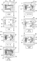
도 1a는 제조 공정의 추가 단계들의 플로우 다이어그램이다.
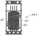
도 2는 제조의 다양한 스테이지들에서 캐리어 상의 디바이스들의 도면이다.
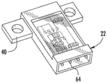
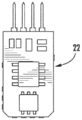
도 3은 캐리어로부터 분리된 완성된 디바이스의 도면이다.
도 4는 릴-투-릴 캐리어를 나타내는 도면이다.
도 5는 기판 상에 전자 회로 트레이스를 생성하기 위한 다중 레이저 연속 공정에 대한 플로우 다이어그램이다.
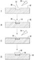
도 6은 조립체의 형성을 도시하는 플로우 차트(flow chart)를 도시한다.
도 7 내지 도 12는 도 6에 도시된 공정을 거쳐 가는 조립체의 실시예를 도시한다.
도 13은 제조 공정에 의해 형성된 자동차 조명기기의 사시도를 도시한다.
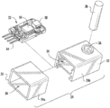
도 14는 자동차 조명기기의 분해 사시도이다.
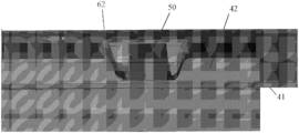
도 15는 캐리어 및 성형된 기판의 일부의 단면도로서, 그 위에 안착된 구성요소를 도시한다.
도 16은 캐리어 및 성형된 기판의 일부의 다른 단면도이다.
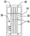
도 17은 베어 다이(bare die), 능동(active), 및 수동(passive) 디바이스들이 성형 및 이미징된(imaged) 기판의 리세스들 내로 패키징된 상태로 릴-투-릴 제조되는 폴리이미드 가요성 코어를 갖는 예시적인 ASEP 적용예의 평면도이다.
도 18은 도 17의 예시적인 ASEP 적용예의 사시도이다.
도 19는 캐리어 및 성형된 기판의 일부의 단면 사시도로서, 그 위에 안착된 구성요소를 도시한다.
도 20은 캐리어 및 성형된 기판의 일부의 단면 사시도로서, 달리 안착된 구성요소를 도시한다.
도 21은 캐리어 및 성형된 기판의 일부의 단면도로서, 그 안에 안착된 구성요소를 도시한다.
도 22는 ASEP 제조 공정의 실시예의 단계들을 보여주는 플로우 차트이다.
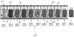
도 23은 ASEP 제조 공정의 실시예의 단계들의 플로우 다이어그램이다.
도 23a 내지 도 23k는 도 23의 플로우 다이어그램의 개별 단계들의 확대도를 도시한다.
특정 실시예들이 앞서 나열된 도면들을 참조하여 아래에서 개시된다. 동일한 도면부호들/참조 기호들이 도면 하나 하나에서 동일한 객체를 나타내려는 것이 아닐 수도 있다. 일부 경우에 그들은 그러하지만, 다른 경우에 그들은 그렇지 않고, 이는 아래의 상세한 설명에서 그들의 사용의 상황에 의해 나타낸 바와 같다.
Claims (16)
- 전자 디바이스들을 제조하는 방법으로서,
전기 전도성 재료로 형성된 연속 캐리어를 형성하는 것;
상기 캐리어 상으로 복수의 비전도성 기판들을 성형하되, 상기 캐리어의 부분들이 노출되도록 포켓들이 상기 기판들 내로 성형되는 것;
상기 기판들 상에 트레이스들을 형성하는 것;
상기 트레이스들을 전기도금하는 것;
복수의 디바이스들을 형성하도록 상기 트레이스들에 구성요소들을 전기적으로 부착하되, 상기 구성요소들 중 적어도 하나는 상기 기판들 내로 성형된 상기 포켓들 중 적어도 하나 내에 안착되는 것; 및
상기 디바이스들 중 하나를 상기 캐리어의 나머지로부터 싱귤레이션하는 것을 포함하는, 전자 디바이스들을 제조하는 방법. - 제1항에 있어서, 상기 트레이스들을 형성하는 것은,
레이저로 상기 기판을 융삭하는 것;
상기 융삭된 표면 상에 잉크를 침착하는 것; 및
상기 잉크를 소결하는 것을 포함하는, 전자 디바이스들을 제조하는 방법. - 제1항에 있어서, 상기 트레이스들을 형성하는 것은 레이저로 전도성 트레이스들을 형성하는 것을 포함하는, 전자 디바이스들을 제조하는 방법.
- 싱귤레이션된 캐리어 부분;
상기 싱귤레이션된 캐리어 부분 상으로 성형된 기판;
상기 기판 상의 시드 층 트레이스들;
상기 시드 층 트레이스들 상의 도금된 금속 트레이스들; 및
적어도 하나의 도금된 금속 트레이스에 전기적으로 부착된 구성요소를 포함하고,
상기 구성요소는 상기 기판 내에 형성된 포켓 내에 안착되고,
상기 포켓은 상기 싱귤레이션된 캐리어 부분의 일부가 노출되도록 상기 기판 내에 형성되는, 디바이스. - 제4항에 있어서, 상기 디바이스는 인쇄 회로 기판, 플렉스 회로(flex circuit), 커넥터, 열 관리 특징부, EMI 차폐부, 고전류 전도체, RFID 장치, 안테나, 무선 급전 디바이스, 센서, MEMS 장치, LED 디바이스, 마이크로프로세서, 메모리 디바이스, ASIC, 수동(passive) 디바이스, 임피던스 제어 디바이스, 및 전기-기계 장치 중 적어도 하나를 포함하는, 디바이스.
- 제4항에 있어서, 상기 싱귤레이션된 캐리어 부분은 금속을 포함하는, 디바이스.
- 제4항에 있어서, 상기 싱귤레이션된 캐리어 부분은 플렉스 재료를 포함하는, 디바이스.
- 제7항에 있어서, 상기 플렉스 재료는 폴리이미드 플렉스 재료를 포함하는, 디바이스.
- 제4항에 있어서, 상기 도금된 금속 트레이스들은 전기도금된 도금된 금속 트레이스들을 포함하는, 디바이스.
- 제4항에 있어서, 상기 시드 층 트레이스들은 소결된 잉크를 포함하는, 디바이스.
- 제4항에 있어서, 상기 시드 층 트레이스들은 소결된 페이스트를 포함하는, 디바이스.
- 싱귤레이션된 캐리어 부분;
상기 싱귤레이션된 캐리어 부분 상으로 성형된 기판;
레이저 및 전기 도금을 통해 상기 기판 상에 형성된 전도성 트레이스들; 및
상기 전도성 트레이스들 중 적어도 하나에 전기적으로 결합된 구성요소를 포함하고,
상기 구성요소는 상기 기판 내에 형성된 포켓 내에 안착되고,
상기 포켓은 상기 싱귤레이션된 캐리어 부분의 일부가 노출되도록 상기 기판 내에 형성되는, 디바이스. - 제12항에 있어서, 상기 디바이스는 인쇄 회로 기판, 플렉스 회로, 커넥터, 열 관리 특징부, EMI 차폐부, 고전류 전도체, RFID 장치, 안테나, 무선 급전 디바이스, 센서, MEMS 장치, LED 디바이스, 마이크로프로세서, 메모리 디바이스, ASIC, 수동 디바이스, 임피던스 제어 디바이스, 및 전기-기계 장치 중 적어도 하나를 포함하는, 디바이스.
- 제12항에 있어서, 상기 싱귤레이션된 캐리어 부분은 금속을 포함하는, 디바이스.
- 제12항에 있어서, 상기 싱귤레이션된 캐리어 부분은 플렉스 재료를 포함하는, 디바이스.
- 제15항에 있어서, 상기 플렉스 재료는 폴리이미드 플렉스 재료를 포함하는, 디바이스.
Priority Applications (1)
| Application Number | Priority Date | Filing Date | Title |
|---|---|---|---|
| KR1020217023239A KR102439790B1 (ko) | 2015-06-29 | 2016-06-28 | 애플리케이션 특정 전자기기 패키징 시스템, 방법 및 디바이스 |
Applications Claiming Priority (10)
| Application Number | Priority Date | Filing Date | Title |
|---|---|---|---|
| US201562186102P | 2015-06-29 | 2015-06-29 | |
| US62/186,102 | 2015-06-29 | ||
| US201562254574P | 2015-11-12 | 2015-11-12 | |
| US62/254,574 | 2015-11-12 | ||
| US201562256477P | 2015-11-17 | 2015-11-17 | |
| US62/256,477 | 2015-11-17 | ||
| US201662326539P | 2016-04-22 | 2016-04-22 | |
| US62/326,539 | 2016-04-22 | ||
| PCT/US2016/039860 WO2017004064A1 (en) | 2015-06-29 | 2016-06-28 | Application specific electronics packaging systems, methods and devices |
| KR1020187002708A KR102143400B1 (ko) | 2015-06-29 | 2016-06-28 | 애플리케이션 특정 전자기기 패키징 시스템, 방법 및 디바이스 |
Related Parent Applications (1)
| Application Number | Title | Priority Date | Filing Date |
|---|---|---|---|
| KR1020187002708A Division KR102143400B1 (ko) | 2015-06-29 | 2016-06-28 | 애플리케이션 특정 전자기기 패키징 시스템, 방법 및 디바이스 |
Related Child Applications (1)
| Application Number | Title | Priority Date | Filing Date |
|---|---|---|---|
| KR1020217023239A Division KR102439790B1 (ko) | 2015-06-29 | 2016-06-28 | 애플리케이션 특정 전자기기 패키징 시스템, 방법 및 디바이스 |
Publications (2)
| Publication Number | Publication Date |
|---|---|
| KR20200096683A true KR20200096683A (ko) | 2020-08-12 |
| KR102282488B1 KR102282488B1 (ko) | 2021-07-28 |
Family
ID=57379833
Family Applications (4)
| Application Number | Title | Priority Date | Filing Date |
|---|---|---|---|
| KR1020217023239A Active KR102439790B1 (ko) | 2015-06-29 | 2016-06-28 | 애플리케이션 특정 전자기기 패키징 시스템, 방법 및 디바이스 |
| KR1020227029996A Active KR102625466B1 (ko) | 2015-06-29 | 2016-06-28 | 애플리케이션 특정 전자기기 패키징 시스템, 방법 및 디바이스 |
| KR1020187002708A Active KR102143400B1 (ko) | 2015-06-29 | 2016-06-28 | 애플리케이션 특정 전자기기 패키징 시스템, 방법 및 디바이스 |
| KR1020207022507A Active KR102282488B1 (ko) | 2015-06-29 | 2016-06-28 | 애플리케이션 특정 전자기기 패키징 시스템, 방법 및 디바이스 |
Family Applications Before (3)
| Application Number | Title | Priority Date | Filing Date |
|---|---|---|---|
| KR1020217023239A Active KR102439790B1 (ko) | 2015-06-29 | 2016-06-28 | 애플리케이션 특정 전자기기 패키징 시스템, 방법 및 디바이스 |
| KR1020227029996A Active KR102625466B1 (ko) | 2015-06-29 | 2016-06-28 | 애플리케이션 특정 전자기기 패키징 시스템, 방법 및 디바이스 |
| KR1020187002708A Active KR102143400B1 (ko) | 2015-06-29 | 2016-06-28 | 애플리케이션 특정 전자기기 패키징 시스템, 방법 및 디바이스 |
Country Status (7)
| Country | Link |
|---|---|
| US (4) | US10433428B2 (ko) |
| EP (1) | EP3314991A4 (ko) |
| JP (2) | JP6742352B2 (ko) |
| KR (4) | KR102439790B1 (ko) |
| CN (3) | CN205746638U (ko) |
| TW (1) | TWI656663B (ko) |
| WO (1) | WO2017004064A1 (ko) |
Families Citing this family (15)
| Publication number | Priority date | Publication date | Assignee | Title |
|---|---|---|---|---|
| WO2017004064A1 (en) | 2015-06-29 | 2017-01-05 | Molex, Llc | Application specific electronics packaging systems, methods and devices |
| TWI652871B (zh) * | 2016-07-07 | 2019-03-01 | 莫仕有限公司 | 微型配電盒及其製造方法 |
| WO2019036362A1 (en) | 2017-08-16 | 2019-02-21 | Molex, Llc | ELECTRICAL CONNECTOR ASSEMBLY |
| TWI730604B (zh) * | 2019-01-22 | 2021-06-11 | 美商莫仕有限公司 | 使用專用電子封裝製造工藝的智能連接器及其製造方法 |
| EP4110885A4 (en) * | 2020-02-26 | 2024-04-24 | Ticona LLC | ELECTRONIC DEVICE |
| JP2023514988A (ja) * | 2020-02-26 | 2023-04-12 | ティコナ・エルエルシー | 電子デバイス用ポリマー組成物 |
| JP7737383B2 (ja) * | 2020-02-26 | 2025-09-10 | ティコナ・エルエルシー | 電子デバイス |
| KR20220145385A (ko) | 2020-02-26 | 2022-10-28 | 티코나 엘엘씨 | 회로 구조체 |
| US11728065B2 (en) * | 2020-07-28 | 2023-08-15 | Ticona Llc | Molded interconnect device |
| US11728559B2 (en) | 2021-02-18 | 2023-08-15 | Ticona Llc | Polymer composition for use in an antenna system |
| DE112022004533T5 (de) * | 2021-09-22 | 2024-08-01 | KSR IP Holdings, LLC | Pedalbaugruppe mit mehrfach-schichten aus unterschiedlichen typen von umspritzungsmaterialien |
| CN216354438U (zh) * | 2021-10-29 | 2022-04-19 | 宁德时代新能源科技股份有限公司 | 自加热控制电路和系统 |
| US12247116B2 (en) | 2021-12-01 | 2025-03-11 | Ticona Llc | Antenna module |
| US20250070525A1 (en) * | 2022-03-07 | 2025-02-27 | Molex, Llc | Electrical connector for coupling conductors to an electronic component |
| US12169055B2 (en) | 2023-03-21 | 2024-12-17 | Wes Fannin | LED luminaire with improved updating and replacement characteristics |
Citations (2)
| Publication number | Priority date | Publication date | Assignee | Title |
|---|---|---|---|---|
| JP2010140820A (ja) * | 2008-12-12 | 2010-06-24 | Toshiba Corp | 灯具、配線基板及び配線基板の製造方法 |
| JP2014027265A (ja) * | 2012-06-19 | 2014-02-06 | Taiyo Holdings Co Ltd | プリント配線板の回路形成方法、熱硬化性樹脂組成物、及びプリント配線板 |
Family Cites Families (40)
| Publication number | Priority date | Publication date | Assignee | Title |
|---|---|---|---|---|
| US4689103A (en) * | 1985-11-18 | 1987-08-25 | E. I. Du Pont De Nemours And Company | Method of manufacturing injection molded printed circuit boards in a common planar array |
| US4954872A (en) * | 1988-04-29 | 1990-09-04 | Altair International, Inc. | Electrical contact stabilizer assembly |
| US5283717A (en) * | 1992-12-04 | 1994-02-01 | Sgs-Thomson Microelectronics, Inc. | Circuit assembly having interposer lead frame |
| JPH0818170A (ja) * | 1994-06-28 | 1996-01-19 | Honda Motor Co Ltd | 配線基板 |
| DE19535777A1 (de) * | 1995-09-26 | 1997-03-27 | Siemens Ag | Optoelektronisches Halbleiter-Bauelement und Verfahren zur Herstellung |
| JPH09274121A (ja) * | 1996-04-02 | 1997-10-21 | Shinko Electric Ind Co Ltd | 光用半導体装置とその製造方法 |
| DE19623826C2 (de) * | 1996-06-14 | 2000-06-15 | Siemens Ag | Verfahren zur Herstellung eines Trägerelements für Halbleiterchips |
| JP3543189B2 (ja) | 1997-12-10 | 2004-07-14 | 日本オプネクスト株式会社 | 半導体素子パッケージおよび半導体装置 |
| JPH11195851A (ja) * | 1997-12-26 | 1999-07-21 | Hitachi Cable Ltd | 成形基板 |
| JP3675364B2 (ja) * | 2001-05-30 | 2005-07-27 | ソニー株式会社 | 半導体装置用基板その製造方法および半導体装置 |
| US6664615B1 (en) | 2001-11-20 | 2003-12-16 | National Semiconductor Corporation | Method and apparatus for lead-frame based grid array IC packaging |
| KR100623867B1 (ko) * | 2004-12-31 | 2006-09-14 | 동부일렉트로닉스 주식회사 | 반도체 회로기판의 레이아웃 방법 |
| US7256479B2 (en) * | 2005-01-13 | 2007-08-14 | Fairchild Semiconductor Corporation | Method to manufacture a universal footprint for a package with exposed chip |
| EP1897146A2 (en) * | 2005-06-27 | 2008-03-12 | Lamina Lighting, Inc. | Light emitting diode package and method for making same |
| JP4549939B2 (ja) * | 2005-06-28 | 2010-09-22 | 日東電工株式会社 | 配線回路基板保持シート |
| JP2007071980A (ja) * | 2005-09-05 | 2007-03-22 | Mitsubishi Electric Corp | 光モジュール |
| US7341365B2 (en) * | 2005-12-16 | 2008-03-11 | Ford Global Technologies, Llc | LED unit for a vehicle lamp assembly |
| US8624129B2 (en) * | 2006-01-12 | 2014-01-07 | Samsung Electronics Co., Ltd. | Method of attaching a high power surface mount transistor to a printed circuit board |
| JP2007273533A (ja) * | 2006-03-30 | 2007-10-18 | Sumitomo Heavy Ind Ltd | 導電パターンの形成方法及び形成装置 |
| US7763478B2 (en) * | 2006-08-21 | 2010-07-27 | Cree, Inc. | Methods of forming semiconductor light emitting device packages by liquid injection molding |
| US7592691B2 (en) * | 2006-09-01 | 2009-09-22 | Micron Technology, Inc. | High density stacked die assemblies, structures incorporated therein and methods of fabricating the assemblies |
| JP2008263118A (ja) * | 2007-04-13 | 2008-10-30 | Nec Lighting Ltd | 発光デバイス |
| KR100937136B1 (ko) * | 2007-12-24 | 2010-01-18 | (주)루미브라이트 | 복수의 패키지를 모듈화한 리드프레임을 이용한 발광다이오드 모듈 |
| US7836586B2 (en) | 2008-08-21 | 2010-11-23 | National Semiconductor Corporation | Thin foil semiconductor package |
| US8021919B2 (en) * | 2009-03-31 | 2011-09-20 | Infineon Technologies Ag | Method of manufacturing a semiconductor device |
| US7955873B2 (en) * | 2009-03-31 | 2011-06-07 | Infineon Technologies Ag | Method of fabricating a semiconductor device |
| CN102236820A (zh) * | 2010-04-27 | 2011-11-09 | 上海长丰智能卡有限公司 | 一种带负载电容的微型射频模块及其封装方法 |
| JP5502647B2 (ja) * | 2010-08-06 | 2014-05-28 | 日東電工株式会社 | 配線回路基板集合体シートおよびその製造方法 |
| US8389334B2 (en) * | 2010-08-17 | 2013-03-05 | National Semiconductor Corporation | Foil-based method for packaging intergrated circuits |
| CN202012788U (zh) | 2011-04-28 | 2011-10-19 | 东莞勤上光电股份有限公司 | 一种led照明设备 |
| EP2754597A4 (en) | 2011-09-05 | 2015-03-04 | Honda Motor Co Ltd | CONTROL DEVICE AND CONTROL METHOD FOR HYBRID VEHICLE |
| CN103294249B (zh) * | 2012-08-17 | 2016-05-18 | 上海天马微电子有限公司 | 触摸屏的制造方法 |
| CN103426776A (zh) * | 2013-07-09 | 2013-12-04 | 上海百嘉电子有限公司 | 智能卡载带的制造方法 |
| US9829159B2 (en) | 2013-08-23 | 2017-11-28 | Molex, Llc | LED module |
| US9318411B2 (en) * | 2013-11-13 | 2016-04-19 | Brodge Semiconductor Corporation | Semiconductor package with package-on-package stacking capability and method of manufacturing the same |
| CN104851812B (zh) * | 2014-02-19 | 2017-10-20 | 钰桥半导体股份有限公司 | 半导体元件及其制作方法 |
| US9733304B2 (en) * | 2014-09-24 | 2017-08-15 | Micron Technology, Inc. | Semiconductor device test apparatuses |
| US9252337B1 (en) * | 2014-12-22 | 2016-02-02 | Bridgelux, Inc. | Composite substrate for light emitting diodes |
| CN105789058A (zh) * | 2015-01-14 | 2016-07-20 | 钰桥半导体股份有限公司 | 中介层嵌置于加强层中的线路板及其制作方法 |
| WO2017004064A1 (en) * | 2015-06-29 | 2017-01-05 | Molex, Llc | Application specific electronics packaging systems, methods and devices |
-
2016
- 2016-06-28 WO PCT/US2016/039860 patent/WO2017004064A1/en not_active Ceased
- 2016-06-28 EP EP16818608.8A patent/EP3314991A4/en active Pending
- 2016-06-28 JP JP2017568255A patent/JP6742352B2/ja active Active
- 2016-06-28 KR KR1020217023239A patent/KR102439790B1/ko active Active
- 2016-06-28 KR KR1020227029996A patent/KR102625466B1/ko active Active
- 2016-06-28 KR KR1020187002708A patent/KR102143400B1/ko active Active
- 2016-06-28 KR KR1020207022507A patent/KR102282488B1/ko active Active
- 2016-06-28 US US15/737,935 patent/US10433428B2/en active Active
- 2016-06-29 TW TW105120444A patent/TWI656663B/zh active
- 2016-06-29 CN CN201620672647.3U patent/CN205746638U/zh not_active Expired - Fee Related
- 2016-06-29 CN CN202111613301.8A patent/CN114234138B/zh active Active
- 2016-06-29 CN CN201610500213.XA patent/CN106287589B/zh active Active
-
2019
- 2019-09-24 US US16/579,890 patent/US10667407B2/en active Active
-
2020
- 2020-04-21 JP JP2020075175A patent/JP7127083B2/ja active Active
- 2020-05-22 US US16/881,017 patent/US10905014B2/en active Active
-
2021
- 2021-01-20 US US17/152,804 patent/US11503718B2/en active Active
Patent Citations (2)
| Publication number | Priority date | Publication date | Assignee | Title |
|---|---|---|---|---|
| JP2010140820A (ja) * | 2008-12-12 | 2010-06-24 | Toshiba Corp | 灯具、配線基板及び配線基板の製造方法 |
| JP2014027265A (ja) * | 2012-06-19 | 2014-02-06 | Taiyo Holdings Co Ltd | プリント配線板の回路形成方法、熱硬化性樹脂組成物、及びプリント配線板 |
Also Published As
| Publication number | Publication date |
|---|---|
| KR102439790B1 (ko) | 2022-09-02 |
| KR102282488B1 (ko) | 2021-07-28 |
| US10667407B2 (en) | 2020-05-26 |
| US10433428B2 (en) | 2019-10-01 |
| JP2018532251A (ja) | 2018-11-01 |
| WO2017004064A1 (en) | 2017-01-05 |
| CN114234138B (zh) | 2025-05-30 |
| CN106287589A (zh) | 2017-01-04 |
| US20200022265A1 (en) | 2020-01-16 |
| TWI656663B (zh) | 2019-04-11 |
| JP7127083B2 (ja) | 2022-08-29 |
| US11503718B2 (en) | 2022-11-15 |
| JP2020120125A (ja) | 2020-08-06 |
| US20180184526A1 (en) | 2018-06-28 |
| EP3314991A4 (en) | 2019-03-27 |
| US10905014B2 (en) | 2021-01-26 |
| JP6742352B2 (ja) | 2020-08-19 |
| EP3314991A1 (en) | 2018-05-02 |
| KR20220124823A (ko) | 2022-09-14 |
| KR20210094162A (ko) | 2021-07-28 |
| KR20180016611A (ko) | 2018-02-14 |
| KR102143400B1 (ko) | 2020-08-11 |
| CN114234138A (zh) | 2022-03-25 |
| CN106287589B (zh) | 2024-07-26 |
| TW201709564A (zh) | 2017-03-01 |
| KR102625466B1 (ko) | 2024-01-17 |
| US20200352032A1 (en) | 2020-11-05 |
| CN205746638U (zh) | 2016-11-30 |
| US20210144861A1 (en) | 2021-05-13 |
Similar Documents
| Publication | Publication Date | Title |
|---|---|---|
| US11503718B2 (en) | Application specific electronics packaging systems, methods and devices | |
| US20220059977A1 (en) | Smart connector and method of manufacturing same using an application specific electronics packaging manufacturing process | |
| KR102215095B1 (ko) | 마이크로 배전 박스 및 애플리케이션 특정 전자기기 패키징 기법을 사용한 그의 제조 방법 | |
| KR102221083B1 (ko) | 성형 상호연결 디바이스 및 그 제조 방법 | |
| WO2010136596A3 (en) | Method of manufacturing an electrical circuit on a substrate |
Legal Events
| Date | Code | Title | Description |
|---|---|---|---|
| A107 | Divisional application of patent | ||
| PA0104 | Divisional application for international application |
Comment text: Divisional Application for International Patent Patent event code: PA01041R01D Patent event date: 20200804 Application number text: 1020187002708 Filing date: 20180129 |
|
| PA0201 | Request for examination | ||
| PG1501 | Laying open of application | ||
| E902 | Notification of reason for refusal | ||
| PE0902 | Notice of grounds for rejection |
Comment text: Notification of reason for refusal Patent event date: 20201014 Patent event code: PE09021S01D |
|
| E701 | Decision to grant or registration of patent right | ||
| PE0701 | Decision of registration |
Patent event code: PE07011S01D Comment text: Decision to Grant Registration Patent event date: 20210528 |
|
| A107 | Divisional application of patent | ||
| GRNT | Written decision to grant | ||
| PA0104 | Divisional application for international application |
Comment text: Divisional Application for International Patent Patent event code: PA01041R01D Patent event date: 20210721 Application number text: 1020187002708 Filing date: 20180129 |
|
| PR0701 | Registration of establishment |
Comment text: Registration of Establishment Patent event date: 20210721 Patent event code: PR07011E01D |
|
| PR1002 | Payment of registration fee |
Payment date: 20210722 End annual number: 3 Start annual number: 1 |
|
| PG1601 | Publication of registration | ||
| PR1001 | Payment of annual fee |
Payment date: 20240619 Start annual number: 4 End annual number: 4 |
|
| PR1001 | Payment of annual fee |
Payment date: 20250616 Start annual number: 5 End annual number: 5 |