KR20200098582A - 실장 구조체의 제조방법 및 이것에 이용되는 시트 - Google Patents
실장 구조체의 제조방법 및 이것에 이용되는 시트 Download PDFInfo
- Publication number
- KR20200098582A KR20200098582A KR1020207019574A KR20207019574A KR20200098582A KR 20200098582 A KR20200098582 A KR 20200098582A KR 1020207019574 A KR1020207019574 A KR 1020207019574A KR 20207019574 A KR20207019574 A KR 20207019574A KR 20200098582 A KR20200098582 A KR 20200098582A
- Authority
- KR
- South Korea
- Prior art keywords
- sheet
- circuit
- thermosetting
- thermoplastic
- less
- Prior art date
- Legal status (The legal status is an assumption and is not a legal conclusion. Google has not performed a legal analysis and makes no representation as to the accuracy of the status listed.)
- Granted
Links
Images




Classifications
-
- H—ELECTRICITY
- H10—SEMICONDUCTOR DEVICES; ELECTRIC SOLID-STATE DEVICES NOT OTHERWISE PROVIDED FOR
- H10W—GENERIC PACKAGES, INTERCONNECTIONS, CONNECTORS OR OTHER CONSTRUCTIONAL DETAILS OF DEVICES COVERED BY CLASS H10
- H10W74/00—Encapsulations, e.g. protective coatings
- H10W74/01—Manufacture or treatment
- H10W74/019—Manufacture or treatment using temporary auxiliary substrates
-
- H01L23/31—
-
- H—ELECTRICITY
- H10—SEMICONDUCTOR DEVICES; ELECTRIC SOLID-STATE DEVICES NOT OTHERWISE PROVIDED FOR
- H10W—GENERIC PACKAGES, INTERCONNECTIONS, CONNECTORS OR OTHER CONSTRUCTIONAL DETAILS OF DEVICES COVERED BY CLASS H10
- H10W74/00—Encapsulations, e.g. protective coatings
- H10W74/01—Manufacture or treatment
-
- H01L21/56—
-
- H01L23/29—
-
- H—ELECTRICITY
- H03—ELECTRONIC CIRCUITRY
- H03H—IMPEDANCE NETWORKS, e.g. RESONANT CIRCUITS; RESONATORS
- H03H3/00—Apparatus or processes specially adapted for the manufacture of impedance networks, resonating circuits, resonators
- H03H3/007—Apparatus or processes specially adapted for the manufacture of impedance networks, resonating circuits, resonators for the manufacture of electromechanical resonators or networks
- H03H3/08—Apparatus or processes specially adapted for the manufacture of impedance networks, resonating circuits, resonators for the manufacture of electromechanical resonators or networks for the manufacture of resonators or networks using surface acoustic waves
-
- H—ELECTRICITY
- H03—ELECTRONIC CIRCUITRY
- H03H—IMPEDANCE NETWORKS, e.g. RESONANT CIRCUITS; RESONATORS
- H03H9/00—Networks comprising electromechanical or electro-acoustic elements; Electromechanical resonators
- H03H9/02—Details
- H03H9/05—Holders or supports
- H03H9/10—Mounting in enclosures
- H03H9/1064—Mounting in enclosures for surface acoustic wave [SAW] devices
- H03H9/1078—Mounting in enclosures for surface acoustic wave [SAW] devices the enclosure being defined by a foil covering the non-active sides of the SAW device
-
- H—ELECTRICITY
- H03—ELECTRONIC CIRCUITRY
- H03H—IMPEDANCE NETWORKS, e.g. RESONANT CIRCUITS; RESONATORS
- H03H9/00—Networks comprising electromechanical or electro-acoustic elements; Electromechanical resonators
- H03H9/25—Constructional features of resonators using surface acoustic waves
-
- H—ELECTRICITY
- H05—ELECTRIC TECHNIQUES NOT OTHERWISE PROVIDED FOR
- H05K—PRINTED CIRCUITS; CASINGS OR CONSTRUCTIONAL DETAILS OF ELECTRIC APPARATUS; MANUFACTURE OF ASSEMBLAGES OF ELECTRICAL COMPONENTS
- H05K1/00—Printed circuits
- H05K1/02—Details
- H05K1/14—Structural association of two or more printed circuits
- H05K1/144—Stacked arrangements of planar printed circuit boards
-
- H—ELECTRICITY
- H05—ELECTRIC TECHNIQUES NOT OTHERWISE PROVIDED FOR
- H05K—PRINTED CIRCUITS; CASINGS OR CONSTRUCTIONAL DETAILS OF ELECTRIC APPARATUS; MANUFACTURE OF ASSEMBLAGES OF ELECTRICAL COMPONENTS
- H05K3/00—Apparatus or processes for manufacturing printed circuits
- H05K3/46—Manufacturing multilayer circuits
- H05K3/4611—Manufacturing multilayer circuits by laminating two or more circuit boards
- H05K3/4626—Manufacturing multilayer circuits by laminating two or more circuit boards characterised by the insulating layers or materials
- H05K3/4632—Manufacturing multilayer circuits by laminating two or more circuit boards characterised by the insulating layers or materials laminating thermoplastic or uncured resin sheets comprising printed circuits without added adhesive materials between the sheets
-
- H—ELECTRICITY
- H10—SEMICONDUCTOR DEVICES; ELECTRIC SOLID-STATE DEVICES NOT OTHERWISE PROVIDED FOR
- H10W—GENERIC PACKAGES, INTERCONNECTIONS, CONNECTORS OR OTHER CONSTRUCTIONAL DETAILS OF DEVICES COVERED BY CLASS H10
- H10W42/00—Arrangements for protection of devices
- H10W42/20—Arrangements for protection of devices protecting against electromagnetic or particle radiation, e.g. light, X-rays, gamma-rays or electrons
-
- H—ELECTRICITY
- H10—SEMICONDUCTOR DEVICES; ELECTRIC SOLID-STATE DEVICES NOT OTHERWISE PROVIDED FOR
- H10W—GENERIC PACKAGES, INTERCONNECTIONS, CONNECTORS OR OTHER CONSTRUCTIONAL DETAILS OF DEVICES COVERED BY CLASS H10
- H10W42/00—Arrangements for protection of devices
- H10W42/20—Arrangements for protection of devices protecting against electromagnetic or particle radiation, e.g. light, X-rays, gamma-rays or electrons
- H10W42/261—Arrangements for protection of devices protecting against electromagnetic or particle radiation, e.g. light, X-rays, gamma-rays or electrons characterised by their shapes or dispositions
- H10W42/276—Arrangements for protection of devices protecting against electromagnetic or particle radiation, e.g. light, X-rays, gamma-rays or electrons characterised by their shapes or dispositions the arrangements being on an external surface of the package, e.g. on the outer surface of an encapsulation
-
- H—ELECTRICITY
- H10—SEMICONDUCTOR DEVICES; ELECTRIC SOLID-STATE DEVICES NOT OTHERWISE PROVIDED FOR
- H10W—GENERIC PACKAGES, INTERCONNECTIONS, CONNECTORS OR OTHER CONSTRUCTIONAL DETAILS OF DEVICES COVERED BY CLASS H10
- H10W42/00—Arrangements for protection of devices
- H10W42/20—Arrangements for protection of devices protecting against electromagnetic or particle radiation, e.g. light, X-rays, gamma-rays or electrons
- H10W42/281—Arrangements for protection of devices protecting against electromagnetic or particle radiation, e.g. light, X-rays, gamma-rays or electrons characterised by their materials
- H10W42/284—Arrangements for protection of devices protecting against electromagnetic or particle radiation, e.g. light, X-rays, gamma-rays or electrons characterised by their materials shielding resins
-
- H—ELECTRICITY
- H10—SEMICONDUCTOR DEVICES; ELECTRIC SOLID-STATE DEVICES NOT OTHERWISE PROVIDED FOR
- H10W—GENERIC PACKAGES, INTERCONNECTIONS, CONNECTORS OR OTHER CONSTRUCTIONAL DETAILS OF DEVICES COVERED BY CLASS H10
- H10W70/00—Package substrates; Interposers; Redistribution layers [RDL]
- H10W70/60—Insulating or insulated package substrates; Interposers; Redistribution layers
-
- H—ELECTRICITY
- H10—SEMICONDUCTOR DEVICES; ELECTRIC SOLID-STATE DEVICES NOT OTHERWISE PROVIDED FOR
- H10W—GENERIC PACKAGES, INTERCONNECTIONS, CONNECTORS OR OTHER CONSTRUCTIONAL DETAILS OF DEVICES COVERED BY CLASS H10
- H10W74/00—Encapsulations, e.g. protective coatings
- H10W74/01—Manufacture or treatment
- H10W74/014—Manufacture or treatment using batch processing
-
- H—ELECTRICITY
- H10—SEMICONDUCTOR DEVICES; ELECTRIC SOLID-STATE DEVICES NOT OTHERWISE PROVIDED FOR
- H10W—GENERIC PACKAGES, INTERCONNECTIONS, CONNECTORS OR OTHER CONSTRUCTIONAL DETAILS OF DEVICES COVERED BY CLASS H10
- H10W74/00—Encapsulations, e.g. protective coatings
- H10W74/10—Encapsulations, e.g. protective coatings characterised by their shape or disposition
-
- H—ELECTRICITY
- H10—SEMICONDUCTOR DEVICES; ELECTRIC SOLID-STATE DEVICES NOT OTHERWISE PROVIDED FOR
- H10W—GENERIC PACKAGES, INTERCONNECTIONS, CONNECTORS OR OTHER CONSTRUCTIONAL DETAILS OF DEVICES COVERED BY CLASS H10
- H10W74/00—Encapsulations, e.g. protective coatings
- H10W74/10—Encapsulations, e.g. protective coatings characterised by their shape or disposition
- H10W74/111—Encapsulations, e.g. protective coatings characterised by their shape or disposition the semiconductor body being completely enclosed
- H10W74/114—Encapsulations, e.g. protective coatings characterised by their shape or disposition the semiconductor body being completely enclosed by a substrate and the encapsulations
-
- H—ELECTRICITY
- H10—SEMICONDUCTOR DEVICES; ELECTRIC SOLID-STATE DEVICES NOT OTHERWISE PROVIDED FOR
- H10W—GENERIC PACKAGES, INTERCONNECTIONS, CONNECTORS OR OTHER CONSTRUCTIONAL DETAILS OF DEVICES COVERED BY CLASS H10
- H10W74/00—Encapsulations, e.g. protective coatings
- H10W74/40—Encapsulations, e.g. protective coatings characterised by their materials
-
- H—ELECTRICITY
- H10—SEMICONDUCTOR DEVICES; ELECTRIC SOLID-STATE DEVICES NOT OTHERWISE PROVIDED FOR
- H10W—GENERIC PACKAGES, INTERCONNECTIONS, CONNECTORS OR OTHER CONSTRUCTIONAL DETAILS OF DEVICES COVERED BY CLASS H10
- H10W74/00—Encapsulations, e.g. protective coatings
- H10W74/40—Encapsulations, e.g. protective coatings characterised by their materials
- H10W74/47—Encapsulations, e.g. protective coatings characterised by their materials comprising organic materials, e.g. plastics or resins
-
- H—ELECTRICITY
- H10—SEMICONDUCTOR DEVICES; ELECTRIC SOLID-STATE DEVICES NOT OTHERWISE PROVIDED FOR
- H10W—GENERIC PACKAGES, INTERCONNECTIONS, CONNECTORS OR OTHER CONSTRUCTIONAL DETAILS OF DEVICES COVERED BY CLASS H10
- H10W90/00—Package configurations
-
- H01L2224/16225—
-
- H—ELECTRICITY
- H03—ELECTRONIC CIRCUITRY
- H03H—IMPEDANCE NETWORKS, e.g. RESONANT CIRCUITS; RESONATORS
- H03H9/00—Networks comprising electromechanical or electro-acoustic elements; Electromechanical resonators
- H03H9/02—Details
- H03H9/05—Holders or supports
- H03H9/10—Mounting in enclosures
-
- H—ELECTRICITY
- H05—ELECTRIC TECHNIQUES NOT OTHERWISE PROVIDED FOR
- H05K—PRINTED CIRCUITS; CASINGS OR CONSTRUCTIONAL DETAILS OF ELECTRIC APPARATUS; MANUFACTURE OF ASSEMBLAGES OF ELECTRICAL COMPONENTS
- H05K2203/00—Indexing scheme relating to apparatus or processes for manufacturing printed circuits covered by H05K3/00
- H05K2203/06—Lamination
- H05K2203/068—Features of the lamination press or of the lamination process, e.g. using special separator sheets
-
- H—ELECTRICITY
- H05—ELECTRIC TECHNIQUES NOT OTHERWISE PROVIDED FOR
- H05K—PRINTED CIRCUITS; CASINGS OR CONSTRUCTIONAL DETAILS OF ELECTRIC APPARATUS; MANUFACTURE OF ASSEMBLAGES OF ELECTRICAL COMPONENTS
- H05K2203/00—Indexing scheme relating to apparatus or processes for manufacturing printed circuits covered by H05K3/00
- H05K2203/11—Treatments characterised by their effect, e.g. heating, cooling, roughening
- H05K2203/1147—Sealing or impregnating, e.g. of pores
-
- H—ELECTRICITY
- H10—SEMICONDUCTOR DEVICES; ELECTRIC SOLID-STATE DEVICES NOT OTHERWISE PROVIDED FOR
- H10W—GENERIC PACKAGES, INTERCONNECTIONS, CONNECTORS OR OTHER CONSTRUCTIONAL DETAILS OF DEVICES COVERED BY CLASS H10
- H10W72/00—Interconnections or connectors in packages
- H10W72/01—Manufacture or treatment
- H10W72/0198—Manufacture or treatment batch processes
-
- H—ELECTRICITY
- H10—SEMICONDUCTOR DEVICES; ELECTRIC SOLID-STATE DEVICES NOT OTHERWISE PROVIDED FOR
- H10W—GENERIC PACKAGES, INTERCONNECTIONS, CONNECTORS OR OTHER CONSTRUCTIONAL DETAILS OF DEVICES COVERED BY CLASS H10
- H10W72/00—Interconnections or connectors in packages
- H10W72/20—Bump connectors, e.g. solder bumps or copper pillars; Dummy bumps; Thermal bumps
- H10W72/251—Materials
- H10W72/252—Materials comprising solid metals or solid metalloids, e.g. PbSn, Ag or Cu
-
- H—ELECTRICITY
- H10—SEMICONDUCTOR DEVICES; ELECTRIC SOLID-STATE DEVICES NOT OTHERWISE PROVIDED FOR
- H10W—GENERIC PACKAGES, INTERCONNECTIONS, CONNECTORS OR OTHER CONSTRUCTIONAL DETAILS OF DEVICES COVERED BY CLASS H10
- H10W90/00—Package configurations
- H10W90/701—Package configurations characterised by the relative positions of pads or connectors relative to package parts
- H10W90/721—Package configurations characterised by the relative positions of pads or connectors relative to package parts of bump connectors
- H10W90/722—Package configurations characterised by the relative positions of pads or connectors relative to package parts of bump connectors between stacked chips
-
- H—ELECTRICITY
- H10—SEMICONDUCTOR DEVICES; ELECTRIC SOLID-STATE DEVICES NOT OTHERWISE PROVIDED FOR
- H10W—GENERIC PACKAGES, INTERCONNECTIONS, CONNECTORS OR OTHER CONSTRUCTIONAL DETAILS OF DEVICES COVERED BY CLASS H10
- H10W90/00—Package configurations
- H10W90/701—Package configurations characterised by the relative positions of pads or connectors relative to package parts
- H10W90/721—Package configurations characterised by the relative positions of pads or connectors relative to package parts of bump connectors
- H10W90/724—Package configurations characterised by the relative positions of pads or connectors relative to package parts of bump connectors between a chip and a stacked insulating package substrate, interposer or RDL
Landscapes
- Engineering & Computer Science (AREA)
- Physics & Mathematics (AREA)
- Acoustics & Sound (AREA)
- Manufacturing & Machinery (AREA)
- Microelectronics & Electronic Packaging (AREA)
- Structures Or Materials For Encapsulating Or Coating Semiconductor Devices Or Solid State Devices (AREA)
- Laminated Bodies (AREA)
- Encapsulation Of And Coatings For Semiconductor Or Solid State Devices (AREA)
- Piezo-Electric Or Mechanical Vibrators, Or Delay Or Filter Circuits (AREA)
- Surface Acoustic Wave Elements And Circuit Networks Thereof (AREA)
- Replacement Of Web Rolls (AREA)
- Vehicle Interior And Exterior Ornaments, Soundproofing, And Insulation (AREA)
- Conveying And Assembling Of Building Elements In Situ (AREA)
- Bridges Or Land Bridges (AREA)
- Glass Compositions (AREA)
Abstract
Description
도 2는 본 발명의 1실시형태에 관련된 제조방법에 있어서의 배치공정을, 실장부재 혹은 실장 구조체의 단면에 의해 모식적으로 도시하는 설명도이다.
도 3은 본 발명의 1실시형태에 관련된 제조방법에 있어서의 제1 봉지공정을, 실장부재 혹은 실장 구조체의 단면에 의해 모식적으로 도시하는 설명도이다.
도 4는 본 발명의 1실시형태에 관련된 제조방법에 있어서의 제1 봉지공정을, 실장부재 혹은 실장 구조체의 단면에 의해 모식적으로 도시하는 설명도이다.
도 5는 본 발명의 1실시형태에 관련된 제조방법에 있어서의 제1 봉지공정을, 실장부재 혹은 실장 구조체의 단면에 의해 모식적으로 도시하는 설명도이다.
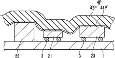
도 6은 본 발명의 1실시형태에 관련된 제조방법에 있어서의 열가소성 시트의 제거공정을, 실장부재 혹은 실장 구조체의 단면에 의해 모식적으로 도시하는 설명도이다.
도 7은 본 발명의 1실시형태에 관련된 제조방법에 있어서의 열가소성 시트의 제거공정을, 실장부재 혹은 실장 구조체의 단면에 의해 모식적으로 도시하는 설명도이다.
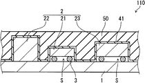
도 8은 본 발명의 1실시형태에 관련된 제조방법에 있어서의 제2 봉지공정을, 실장부재 혹은 실장 구조체의 단면에 의해 모식적으로 도시하는 설명도이다.

1: 제1 회로부재
2: 제2 회로부재
21: 기준부재
22: 제1의 인접부재
23: 제2의 인접부재
3: 범프
S: 내부공간
4P: 시트
41P: 열경화성 시트
42P: 열가소성 시트
41: 열경화성 시트의 경화물(봉지재)
50: 제2 경화성 재료의 경화물
Claims (12)
- 제1 회로부재와, 상기 제1 회로부재에 탑재되는 복수의 제2 회로부재를 구비하는 실장부재를 준비하는 공정과,
열경화성 시트와 열가소성 시트를, 상기 열가소성 시트와 상기 제1 회로부재 사이에 상기 열경화성 시트가 개재하도록 상기 실장부재에 배치하는 배치공정과,
상기 열경화성 시트와 상기 열가소성 시트와의 적층체를 상기 제1 회로부재에 대해서 압압(押壓)함과 동시에, 상기 적층체를 가열해서 상기 제2 회로부재를 봉지하고, 상기 열경화성 시트를 경화시켜서 경화층으로 변환하는 제1 봉지공정과,
상기 경화층으로부터 상기 열가소성 시트를 제거하는 제거공정을 구비하고,
복수의 상기 제2 회로부재의 적어도 1개가, 상기 제1 회로부재와의 사이에 형성되는 공간을 구비하는 중공부재이고,
상기 제1 봉지공정에서는, 상기 공간을 유지하면서, 복수의 상기 제2 회로부재가 봉지되는, 실장 구조체의 제조방법. - 제 1 항에 있어서,
상기 배치공정에 앞서서, 상기 열경화성 시트와 상기 열가소성 시트가 일체화된 시트를 준비하는 공정을 구비하고,
상기 배치공정에 있어서, 상기 시트를 상기 실장부재에 배치하는, 실장 구조체의 제조방법. - 제 1 항 또는 제 2 항에 있어서,
상기 제1 봉지공정에 있어서, 가열 하에서, 상기 적층체가 상기 제1 회로부재에 대해서 압압되는, 실장 구조체의 제조방법. - 제 1 항 내지 제 3 항 중 어느 한 항에 있어서,
상기 열가소성 시트를 구성하는 열가소성 재료는, 상기 열가소성 재료로 형성된 두께 100㎛의 시트에 대해서 측정되는 50% 모듈러스가, 3MPa 이상 8MPa 이하이고, 파단 연신도(elongation)가, 200% 이상 1000% 이하이고, 파단 강도가, 10MPa 이상 30MPa 이하인, 실장 구조체의 제조방법. - 제 1 항 내지 제 4 항 중 어느 한 항에 있어서,
상기 열가소성 시트를 구성하는 열가소성 재료의 융점 또는 유리 전이 온도 tm은, 50℃ 이상 130℃ 이하이고, 또한 상기 제2 회로부재가 봉지될 때의 온도 t보다도 낮은, 실장 구조체의 제조방법. - 제 1 항 내지 제 5 항 중 어느 한 항에 있어서,
상기 제2 회로부재가 봉지될 때의 온도 t에 있어서, 상기 열경화성 시트를 구성하는 열경화성 재료는, 0.1 이상 0.8 이하의 손실 탄젠트 tanδ, 및 1×10⁴Pa 이상 1×10⁷Pa 이하의 저장 전단 탄성률을 나타내는, 실장 구조체의 제조방법. - 제 1 항 내지 제 6 항 중 어느 한 항에 있어서,
서로 인접하는 제2 회로부재의 이간거리가 150㎛ 이하인 제2 회로부재를 적어도 1개 구비하는, 실장 구조체의 제조방법. - 제 1 항 내지 제 7 항 중 어느 한 항에 있어서,
상기 제2 회로부재는, 기준부재와, 상기 기준부재에 각각 인접하는 제1의 인접부재 및 제2의 인접부재를 구비하고,
상기 기준부재와 상기 제1의 인접부재 사이의 이간거리 D1과, 상기 기준부재와 상기 제2의 인접부재 사이의 이간거리 D2는, 다른, 실장 구조체의 제조방법. - 제 1 항 내지 제 8 항 중 어느 한 항에 있어서,
상기 제2 회로부재는, 기준부재와, 상기 기준부재에 각각 인접하는 제1의 인접부재 및 제2의 인접부재를 구비하고,
상기 제1의 인접부재의 상기 기준부재로부터의 높이 ΔH1과, 상기 제2의 인접부재의 상기 기준부재로부터의 높이 ΔH2는, 다른, 실장 구조체의 제조방법. - 제 1 항 내지 제 9 항 중 어느 한 항에 있어서,
상기 제1 봉지공정에 있어서, 상기 적층체에서 상기 제2 회로부재를 봉지함과 동시에, 상기 제2 회로부재의 형상에 추종시켜서 상기 열가소성 시트를 변형시키는, 실장 구조체의 제조방법. - 제1 회로부재와, 상기 제1 회로부재에 탑재되는 복수의 제2 회로부재를 구비하는 실장부재를 봉지하기 위해서 이용되는 시트로서,
복수의 상기 제2 회로부재의 적어도 1개가, 상기 제1 회로부재와의 사이에 형성되는 공간을 구비하는 중공부재이고,
상기 시트가, 열경화성 시트와, 상기 열경화성 시트에 일체화된 열가소성 시트를 구비하고,
상기 제2 회로부재가 봉지될 때의 온도 t에 있어서, 상기 열경화성 시트를 구성하는 열경화성 재료는, 0.1 이상 0.8 이하의 손실 탄젠트 tanδ, 및 1×10⁴Pa 이상 1×10⁷Pa 이하의 저장 전단 탄성률을 나타내는, 시트. - 제 11 항에 있어서,
상기 열가소성 시트를 구성하는 열가소성 재료는, 상기 열가소성 재료로 형성된 두께 100㎛의 시트에 대해서 측정되는 50% 모듈러스가 3MPa 이상 8MPa 이하이고, 파단 연신도가 200% 이상 1000% 이하이고, 파단 강도가 10MPa 이상 30MPa 이하인, 시트.
Applications Claiming Priority (3)
| Application Number | Priority Date | Filing Date | Title |
|---|---|---|---|
| JPJP-P-2017-240021 | 2017-12-14 | ||
| JP2017240021 | 2017-12-14 | ||
| PCT/JP2018/045941 WO2019117258A1 (ja) | 2017-12-14 | 2018-12-13 | 実装構造体の製造方法およびこれに用いられるシート |
Publications (2)
| Publication Number | Publication Date |
|---|---|
| KR20200098582A true KR20200098582A (ko) | 2020-08-20 |
| KR102525372B1 KR102525372B1 (ko) | 2023-04-26 |
Family
ID=66820387
Family Applications (2)
| Application Number | Title | Priority Date | Filing Date |
|---|---|---|---|
| KR1020207019574A Active KR102525372B1 (ko) | 2017-12-14 | 2018-12-13 | 실장 구조체의 제조방법 및 이것에 이용되는 시트 |
| KR1020207019575A Active KR102678902B1 (ko) | 2017-12-14 | 2018-12-13 | 실장 구조체의 제조방법 |
Family Applications After (1)
| Application Number | Title | Priority Date | Filing Date |
|---|---|---|---|
| KR1020207019575A Active KR102678902B1 (ko) | 2017-12-14 | 2018-12-13 | 실장 구조체의 제조방법 |
Country Status (8)
| Country | Link |
|---|---|
| US (2) | US11710645B2 (ko) |
| EP (2) | EP3726570A4 (ko) |
| JP (2) | JP6718106B2 (ko) |
| KR (2) | KR102525372B1 (ko) |
| CN (2) | CN111466021B (ko) |
| SG (2) | SG11202005449YA (ko) |
| TW (2) | TWI770330B (ko) |
| WO (2) | WO2019117259A1 (ko) |
Families Citing this family (10)
| Publication number | Priority date | Publication date | Assignee | Title |
|---|---|---|---|---|
| JP6764149B1 (ja) * | 2018-11-14 | 2020-09-30 | ナガセケムテックス株式会社 | 硬化性樹脂組成物および硬化性シート |
| KR102732191B1 (ko) * | 2019-08-09 | 2024-11-19 | 나가세케무텍쿠스가부시키가이샤 | 몰드 언더필 봉지용의 다층 시트, 몰드 언더필 봉지 방법, 전자 부품 실장 기판 및 전자 부품 실장 기판의 제조 방법 |
| JP7375392B2 (ja) * | 2019-09-06 | 2023-11-08 | 株式会社大真空 | 圧電振動デバイスの製造方法 |
| JP6809624B1 (ja) * | 2020-03-10 | 2021-01-06 | 住友ベークライト株式会社 | 機能層貼付用フィルムセットおよび絶縁フィルム |
| KR102765498B1 (ko) * | 2020-06-23 | 2025-02-12 | 주식회사 엘지에너지솔루션 | 회로 기판 어셈블리 제조 방법, 이에 의해 제조된 회로 기판 어셈블리 및 이를 구비하는 전기 자동차 |
| JP2022137337A (ja) * | 2021-03-09 | 2022-09-22 | キオクシア株式会社 | 半導体装置 |
| JP2022175441A (ja) * | 2021-05-13 | 2022-11-25 | 三安ジャパンテクノロジー株式会社 | デバイスおよびそのデバイスを備えるモジュール |
| JP2023058259A (ja) * | 2021-10-13 | 2023-04-25 | 富士電機株式会社 | 半導体装置の製造方法及び半導体装置 |
| JP7809997B2 (ja) * | 2022-02-08 | 2026-02-03 | 東レ株式会社 | 電子部品の製造方法及び電子部品の製造に用いる積層体 |
| CN118714748A (zh) * | 2023-03-20 | 2024-09-27 | 鹏鼎控股(深圳)股份有限公司 | 柔性电路板及其制备方法 |
Citations (4)
| Publication number | Priority date | Publication date | Assignee | Title |
|---|---|---|---|---|
| JP2004327623A (ja) * | 2003-04-23 | 2004-11-18 | Three M Innovative Properties Co | 封止用フィルム接着剤、封止用フィルム積層体及び封止方法 |
| JP2014057041A (ja) * | 2012-08-16 | 2014-03-27 | Sumitomo Bakelite Co Ltd | 電磁波シールド用フィルム、および電子部品の被覆方法 |
| JP2015053470A (ja) * | 2013-08-07 | 2015-03-19 | 日東電工株式会社 | 中空型電子デバイス封止用樹脂シート及び中空型電子デバイスパッケージの製造方法 |
| JP2015106573A (ja) | 2013-11-28 | 2015-06-08 | 日東電工株式会社 | 中空封止用樹脂シート、及び、中空パッケージの製造方法 |
Family Cites Families (19)
| Publication number | Priority date | Publication date | Assignee | Title |
|---|---|---|---|---|
| US4089721A (en) * | 1977-03-24 | 1978-05-16 | Sauder Woodworking Co. | Method of making a laminate |
| JPH0961456A (ja) | 1995-08-29 | 1997-03-07 | Murata Mfg Co Ltd | 半導体装置 |
| JP2753470B2 (ja) * | 1996-01-30 | 1998-05-20 | 魏 明進 | コンセント保護具 |
| JP2002184884A (ja) | 2000-12-18 | 2002-06-28 | Tdk Corp | 電子装置およびその製造方法 |
| DE10238523B4 (de) | 2002-08-22 | 2014-10-02 | Epcos Ag | Verkapseltes elektronisches Bauelement und Verfahren zur Herstellung |
| JP2004273853A (ja) * | 2003-03-10 | 2004-09-30 | Matsushita Electric Ind Co Ltd | 樹脂層付チップ部品とそれを用いた部品内蔵モジュール及びそれらの製造方法 |
| JP4872587B2 (ja) | 2006-10-12 | 2012-02-08 | 日立化成工業株式会社 | 封止フィルム、及びこれを用いた半導体装置 |
| KR20110105854A (ko) * | 2009-01-09 | 2011-09-27 | 나가세케무텍쿠스가부시키가이샤 | 반도체 패키지의 제조 방법, 반도체 밀봉 방법 및 용제형 반도체 밀봉 에폭시 수지 조성물 |
| KR101250677B1 (ko) | 2011-09-30 | 2013-04-03 | 삼성전기주식회사 | 반도체 패키지 및 그의 제조 방법 |
| JP6119950B2 (ja) | 2011-12-02 | 2017-04-26 | ナガセケムテックス株式会社 | 中空構造電子部品 |
| JP5735029B2 (ja) * | 2013-03-28 | 2015-06-17 | 日東電工株式会社 | 電子デバイス封止用樹脂シート及び電子デバイスパッケージの製造方法 |
| JP5735036B2 (ja) * | 2013-05-23 | 2015-06-17 | 日東電工株式会社 | 電子部品装置の製造方法、及び、積層シート |
| WO2015079887A1 (ja) * | 2013-11-28 | 2015-06-04 | 日東電工株式会社 | 封止用熱硬化性樹脂シート及び中空パッケージの製造方法 |
| US20150235871A1 (en) * | 2014-02-18 | 2015-08-20 | Shin-Etsu Chemical Co., Ltd. | Vacuum laminating apparatus and method for manufacturing semiconductor apparatus |
| JP6318836B2 (ja) * | 2014-05-15 | 2018-05-09 | 三菱ケミカル株式会社 | 転写用基材及び転写シート |
| JP6459019B2 (ja) * | 2014-05-22 | 2019-01-30 | ナガセケムテックス株式会社 | 封止用積層シートおよびその製造方法ならびに封止用積層シートを用いて封止された実装構造体およびその製造方法 |
| JP6903915B2 (ja) | 2015-01-16 | 2021-07-14 | 昭和電工マテリアルズ株式会社 | 熱硬化性樹脂組成物、層間絶縁用樹脂フィルム、複合フィルム、プリント配線板及びその製造方法 |
| JP6282626B2 (ja) * | 2015-11-04 | 2018-02-21 | 日東電工株式会社 | 中空型電子デバイス封止用シート、及び、中空型電子デバイスパッケージの製造方法 |
| JP6467689B2 (ja) * | 2017-03-13 | 2019-02-13 | ナガセケムテックス株式会社 | 中空構造電子部品 |
-
2018
- 2018-12-13 US US16/772,643 patent/US11710645B2/en active Active
- 2018-12-13 KR KR1020207019574A patent/KR102525372B1/ko active Active
- 2018-12-13 EP EP18887772.4A patent/EP3726570A4/en not_active Withdrawn
- 2018-12-13 CN CN201880080289.9A patent/CN111466021B/zh active Active
- 2018-12-13 WO PCT/JP2018/045942 patent/WO2019117259A1/ja not_active Ceased
- 2018-12-13 WO PCT/JP2018/045941 patent/WO2019117258A1/ja not_active Ceased
- 2018-12-13 KR KR1020207019575A patent/KR102678902B1/ko active Active
- 2018-12-13 EP EP18888529.7A patent/EP3726571A4/en not_active Withdrawn
- 2018-12-13 JP JP2019559208A patent/JP6718106B2/ja active Active
- 2018-12-13 JP JP2019559207A patent/JP6718105B2/ja active Active
- 2018-12-13 SG SG11202005449YA patent/SG11202005449YA/en unknown
- 2018-12-13 US US16/772,608 patent/US11315804B2/en active Active
- 2018-12-13 SG SG11202005448UA patent/SG11202005448UA/en unknown
- 2018-12-13 CN CN201880080263.4A patent/CN111480227B/zh active Active
- 2018-12-14 TW TW107145317A patent/TWI770330B/zh active
- 2018-12-14 TW TW107145316A patent/TWI783097B/zh active
Patent Citations (4)
| Publication number | Priority date | Publication date | Assignee | Title |
|---|---|---|---|---|
| JP2004327623A (ja) * | 2003-04-23 | 2004-11-18 | Three M Innovative Properties Co | 封止用フィルム接着剤、封止用フィルム積層体及び封止方法 |
| JP2014057041A (ja) * | 2012-08-16 | 2014-03-27 | Sumitomo Bakelite Co Ltd | 電磁波シールド用フィルム、および電子部品の被覆方法 |
| JP2015053470A (ja) * | 2013-08-07 | 2015-03-19 | 日東電工株式会社 | 中空型電子デバイス封止用樹脂シート及び中空型電子デバイスパッケージの製造方法 |
| JP2015106573A (ja) | 2013-11-28 | 2015-06-08 | 日東電工株式会社 | 中空封止用樹脂シート、及び、中空パッケージの製造方法 |
Also Published As
| Publication number | Publication date |
|---|---|
| CN111480227A (zh) | 2020-07-31 |
| TW201929627A (zh) | 2019-07-16 |
| CN111480227B (zh) | 2024-04-16 |
| JPWO2019117258A1 (ja) | 2020-07-30 |
| CN111466021B (zh) | 2024-04-16 |
| JP6718105B2 (ja) | 2020-07-08 |
| EP3726571A1 (en) | 2020-10-21 |
| WO2019117258A1 (ja) | 2019-06-20 |
| EP3726570A1 (en) | 2020-10-21 |
| KR102678902B1 (ko) | 2024-06-28 |
| TWI770330B (zh) | 2022-07-11 |
| WO2019117259A1 (ja) | 2019-06-20 |
| US11315804B2 (en) | 2022-04-26 |
| SG11202005449YA (en) | 2020-07-29 |
| US20210084775A1 (en) | 2021-03-18 |
| TWI783097B (zh) | 2022-11-11 |
| JPWO2019117259A1 (ja) | 2020-07-27 |
| EP3726571A4 (en) | 2021-09-08 |
| JP6718106B2 (ja) | 2020-07-08 |
| US11710645B2 (en) | 2023-07-25 |
| KR102525372B1 (ko) | 2023-04-26 |
| US20200388509A1 (en) | 2020-12-10 |
| KR20200098583A (ko) | 2020-08-20 |
| EP3726570A4 (en) | 2021-11-03 |
| SG11202005448UA (en) | 2020-07-29 |
| TW201929628A (zh) | 2019-07-16 |
| CN111466021A (zh) | 2020-07-28 |
Similar Documents
| Publication | Publication Date | Title |
|---|---|---|
| KR102525372B1 (ko) | 실장 구조체의 제조방법 및 이것에 이용되는 시트 | |
| KR102513134B1 (ko) | 실장 구조체의 제조 방법 및 이것에 이용되는 시트 | |
| KR102532359B1 (ko) | 실장 구조체의 제조 방법 및 이것에 이용되는 시트 | |
| TWI754103B (zh) | 安裝結構體之製造方法及使用於其之積層片材 | |
| JP6894076B2 (ja) | 実装構造体の製造方法およびこれに用いられる積層シート | |
| JP6865340B2 (ja) | 実装構造体の製造方法およびこれに用いられる積層シート |
Legal Events
| Date | Code | Title | Description |
|---|---|---|---|
| PA0105 | International application |
St.27 status event code: A-0-1-A10-A15-nap-PA0105 |
|
| PG1501 | Laying open of application |
St.27 status event code: A-1-1-Q10-Q12-nap-PG1501 |
|
| A201 | Request for examination | ||
| P11-X000 | Amendment of application requested |
St.27 status event code: A-2-2-P10-P11-nap-X000 |
|
| P13-X000 | Application amended |
St.27 status event code: A-2-2-P10-P13-nap-X000 |
|
| PA0201 | Request for examination |
St.27 status event code: A-1-2-D10-D11-exm-PA0201 |
|
| E701 | Decision to grant or registration of patent right | ||
| PE0701 | Decision of registration |
St.27 status event code: A-1-2-D10-D22-exm-PE0701 |
|
| PR0701 | Registration of establishment |
St.27 status event code: A-2-4-F10-F11-exm-PR0701 |
|
| PR1002 | Payment of registration fee |
St.27 status event code: A-2-2-U10-U12-oth-PR1002 Fee payment year number: 1 |
|
| PG1601 | Publication of registration |
St.27 status event code: A-4-4-Q10-Q13-nap-PG1601 |
|
| P22-X000 | Classification modified |
St.27 status event code: A-4-4-P10-P22-nap-X000 |
|
| P22-X000 | Classification modified |
St.27 status event code: A-4-4-P10-P22-nap-X000 |
|
| PR1001 | Payment of annual fee |
St.27 status event code: A-4-4-U10-U11-oth-PR1001 Fee payment year number: 4 |
|
| U11 | Full renewal or maintenance fee paid |
Free format text: ST27 STATUS EVENT CODE: A-4-4-U10-U11-OTH-PR1001 (AS PROVIDED BY THE NATIONAL OFFICE) Year of fee payment: 4 |