KR20200099116A - 인덕터 - Google Patents
인덕터 Download PDFInfo
- Publication number
- KR20200099116A KR20200099116A KR1020200097239A KR20200097239A KR20200099116A KR 20200099116 A KR20200099116 A KR 20200099116A KR 1020200097239 A KR1020200097239 A KR 1020200097239A KR 20200097239 A KR20200097239 A KR 20200097239A KR 20200099116 A KR20200099116 A KR 20200099116A
- Authority
- KR
- South Korea
- Prior art keywords
- magnetic body
- internal coil
- inductor
- metal layer
- disposed
- Prior art date
- Legal status (The legal status is an assumption and is not a legal conclusion. Google has not performed a legal analysis and makes no representation as to the accuracy of the status listed.)
- Granted
Links
Images



Classifications
-
- H—ELECTRICITY
- H01—ELECTRIC ELEMENTS
- H01F—MAGNETS; INDUCTANCES; TRANSFORMERS; SELECTION OF MATERIALS FOR THEIR MAGNETIC PROPERTIES
- H01F27/00—Details of transformers or inductances, in general
- H01F27/28—Coils; Windings; Conductive connections
- H01F27/29—Terminals; Tapping arrangements for signal inductances
- H01F27/292—Surface mounted devices
-
- H—ELECTRICITY
- H01—ELECTRIC ELEMENTS
- H01B—CABLES; CONDUCTORS; INSULATORS; SELECTION OF MATERIALS FOR THEIR CONDUCTIVE, INSULATING OR DIELECTRIC PROPERTIES
- H01B1/00—Conductors or conductive bodies characterised by the conductive materials; Selection of materials as conductors
- H01B1/02—Conductors or conductive bodies characterised by the conductive materials; Selection of materials as conductors mainly consisting of metals or alloys
-
- H—ELECTRICITY
- H01—ELECTRIC ELEMENTS
- H01F—MAGNETS; INDUCTANCES; TRANSFORMERS; SELECTION OF MATERIALS FOR THEIR MAGNETIC PROPERTIES
- H01F17/00—Fixed inductances of the signal type
- H01F17/0006—Printed inductances
- H01F17/0013—Printed inductances with stacked layers
-
- H—ELECTRICITY
- H01—ELECTRIC ELEMENTS
- H01F—MAGNETS; INDUCTANCES; TRANSFORMERS; SELECTION OF MATERIALS FOR THEIR MAGNETIC PROPERTIES
- H01F27/00—Details of transformers or inductances, in general
- H01F27/24—Magnetic cores
-
- H—ELECTRICITY
- H01—ELECTRIC ELEMENTS
- H01F—MAGNETS; INDUCTANCES; TRANSFORMERS; SELECTION OF MATERIALS FOR THEIR MAGNETIC PROPERTIES
- H01F27/00—Details of transformers or inductances, in general
- H01F27/28—Coils; Windings; Conductive connections
- H01F27/2804—Printed windings
Landscapes
- Engineering & Computer Science (AREA)
- Power Engineering (AREA)
- Microelectronics & Electronic Packaging (AREA)
- Coils Or Transformers For Communication (AREA)
Abstract
Description
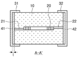
도 2는 도 1의 A-A'선에 의한 단면도이다.
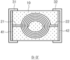
도 3은 도 1의 B-B'선에 의한 단면도이다.
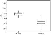
도 4는 본 발명의 실시예와 비교예에 따른 직류 저항(Rdc) 값을 나타내는 그래프이다.
도 5는 본 발명의 다른 실시형태에 따른 도 1의 A-A'선에 의한 단면도이다.
도 6은 도 1의 인덕터의 길이 방향 단부에서 바라본 내부 투시도이다.
도 7은 도 1의 인덕터의 길이 방향 단부에서 바라본 다른 실시형태에 따른 내부 투시도이다.
도 8은 도 1의 인덕터가 회로기판에 실장된 모습을 도시한 사시도이다.
20 : 내부 코일 21, 22 : 인출부
31, 32 : 외부전극 41, 42, 41', 42' : 금속층
200 : 실장 기판 210 ; 회로기판
221, 222 ; 제1 및 제2 전극 패드
230 ; 솔더
Claims (7)
- 자성체 본체;
상기 자성체 본체 내부에 배치된 내부 코일;
상기 내부 코일과 접속되며 상기 자성체 본체의 적어도 일 면으로 노출된 인출부;
상기 인출부 중 상기 자성체 본체로부터 노출된 영역과 접속된 금속층; 및
상기 금속층을 커버하는 외부전극;을 포함하며,
상기 금속층은 상기 자성체 본체에서 상기 인출부가 노출된 면 전체를 커버하며,
상기 금속층은 도금에 의해 형성된 도금층인 인덕터.
- 제1항에 있어서,
상기 금속층은 상기 자성체 본체에서 상기 인출부가 노출된 면 외의 면에서는 상기 자성체 본체를 커버하지 않는 인덕터.
- 제2항에 있어서,
상기 외부전극은 상기 자성체 본체에서 상기 인출부가 노출된 면 외의 면에서 상기 자성체 본체를 커버하는 인덕터.
- 제1항에 있어서,
상기 금속층은 구리(Cu) 및 니켈(Ni) 중 어느 하나 이상을 포함하는 인덕터.
- 제1항에 있어서,
상기 금속층의 두께는 0.5 내지 30 μm인 인덕터.
- 제1항에 있어서,
상기 외부 전극은 은-에폭시(Ag-Epoxy) 및 구리-에폭시(Cu-Epoxy) 중 어느 하나 이상을 포함하는 인덕터.
- 제1항에 있어서,
상기 인출부와 상기 금속층의 접속 면적은 상기 내부 코일의 직경을 r1이라 하면 0.020×r1 (mm2) 이상인 인덕터.
Priority Applications (1)
| Application Number | Priority Date | Filing Date | Title |
|---|---|---|---|
| KR1020200097239A KR102300016B1 (ko) | 2014-07-29 | 2020-08-04 | 인덕터 |
Applications Claiming Priority (2)
| Application Number | Priority Date | Filing Date | Title |
|---|---|---|---|
| KR1020140096351A KR102143005B1 (ko) | 2014-07-29 | 2014-07-29 | 인덕터 및 그 실장 기판 |
| KR1020200097239A KR102300016B1 (ko) | 2014-07-29 | 2020-08-04 | 인덕터 |
Related Parent Applications (1)
| Application Number | Title | Priority Date | Filing Date |
|---|---|---|---|
| KR1020140096351A Division KR102143005B1 (ko) | 2014-07-29 | 2014-07-29 | 인덕터 및 그 실장 기판 |
Publications (2)
| Publication Number | Publication Date |
|---|---|
| KR20200099116A true KR20200099116A (ko) | 2020-08-21 |
| KR102300016B1 KR102300016B1 (ko) | 2021-09-09 |
Family
ID=72235847
Family Applications (1)
| Application Number | Title | Priority Date | Filing Date |
|---|---|---|---|
| KR1020200097239A Active KR102300016B1 (ko) | 2014-07-29 | 2020-08-04 | 인덕터 |
Country Status (1)
| Country | Link |
|---|---|
| KR (1) | KR102300016B1 (ko) |
Citations (5)
| Publication number | Priority date | Publication date | Assignee | Title |
|---|---|---|---|---|
| JPH036005A (ja) * | 1989-06-02 | 1991-01-11 | Tdk Corp | チップ部品端子の低温構成方法 |
| JP2003297646A (ja) * | 2002-04-03 | 2003-10-17 | Matsushita Electric Ind Co Ltd | チップ型電子部品 |
| JP2006278479A (ja) | 2005-03-28 | 2006-10-12 | Tdk Corp | コイル部品 |
| JP2006287063A (ja) * | 2005-04-01 | 2006-10-19 | Murata Mfg Co Ltd | 電子部品 |
| JP2012248629A (ja) * | 2011-05-26 | 2012-12-13 | Tdk Corp | コイル部品及びその製造方法 |
-
2020
- 2020-08-04 KR KR1020200097239A patent/KR102300016B1/ko active Active
Patent Citations (5)
| Publication number | Priority date | Publication date | Assignee | Title |
|---|---|---|---|---|
| JPH036005A (ja) * | 1989-06-02 | 1991-01-11 | Tdk Corp | チップ部品端子の低温構成方法 |
| JP2003297646A (ja) * | 2002-04-03 | 2003-10-17 | Matsushita Electric Ind Co Ltd | チップ型電子部品 |
| JP2006278479A (ja) | 2005-03-28 | 2006-10-12 | Tdk Corp | コイル部品 |
| JP2006287063A (ja) * | 2005-04-01 | 2006-10-19 | Murata Mfg Co Ltd | 電子部品 |
| JP2012248629A (ja) * | 2011-05-26 | 2012-12-13 | Tdk Corp | コイル部品及びその製造方法 |
Also Published As
| Publication number | Publication date |
|---|---|
| KR102300016B1 (ko) | 2021-09-09 |
Similar Documents
| Publication | Publication Date | Title |
|---|---|---|
| KR102143005B1 (ko) | 인덕터 및 그 실장 기판 | |
| KR101983146B1 (ko) | 칩 전자부품 | |
| KR101952859B1 (ko) | 칩 전자부품 및 그 제조방법 | |
| KR101525703B1 (ko) | 칩 전자부품 및 그 제조방법 | |
| JP6213996B2 (ja) | チップ電子部品及びその製造方法 | |
| JP6870804B2 (ja) | コイル部品 | |
| CN110970193B (zh) | 线圈部件 | |
| JP2015079958A (ja) | チップ電子部品、その実装基板及び包装体 | |
| CN108206088B (zh) | 电感器 | |
| US9655247B1 (en) | Coil component and board having the same | |
| KR101823191B1 (ko) | 칩 전자부품 및 그 제조방법 | |
| US20150287514A1 (en) | Chip coil component and board for mounting the same | |
| JP2019153798A (ja) | インダクタ | |
| US10629365B2 (en) | Inductor array component and board for mounting the same | |
| KR101963290B1 (ko) | 코일 부품 | |
| KR102145317B1 (ko) | 칩 전자부품 및 그 제조방법 | |
| US12062476B2 (en) | Chip electronic component and board having the same | |
| KR20140003056A (ko) | 파워 인덕터 및 그 제조방법 | |
| JP6652280B2 (ja) | インダクタ | |
| US9343228B2 (en) | Laminated inductor and manufacturing method thereof | |
| KR102130672B1 (ko) | 적층 전자부품 및 그 제조방법 | |
| KR20170097852A (ko) | 코일 부품 | |
| US20160104563A1 (en) | Chip electronic component | |
| KR102047561B1 (ko) | 칩 전자부품 및 그 실장기판 | |
| KR20160026940A (ko) | 코일 부품 |
Legal Events
| Date | Code | Title | Description |
|---|---|---|---|
| A107 | Divisional application of patent | ||
| A201 | Request for examination | ||
| PA0107 | Divisional application |
St.27 status event code: A-0-1-A10-A18-div-PA0107 St.27 status event code: A-0-1-A10-A16-div-PA0107 |
|
| PA0201 | Request for examination |
St.27 status event code: A-1-2-D10-D11-exm-PA0201 |
|
| PG1501 | Laying open of application |
St.27 status event code: A-1-1-Q10-Q12-nap-PG1501 |
|
| E902 | Notification of reason for refusal | ||
| PE0902 | Notice of grounds for rejection |
St.27 status event code: A-1-2-D10-D21-exm-PE0902 |
|
| AMND | Amendment | ||
| P11-X000 | Amendment of application requested |
St.27 status event code: A-2-2-P10-P11-nap-X000 |
|
| P13-X000 | Application amended |
St.27 status event code: A-2-2-P10-P13-nap-X000 |
|
| E601 | Decision to refuse application | ||
| PE0601 | Decision on rejection of patent |
St.27 status event code: N-2-6-B10-B15-exm-PE0601 |
|
| X091 | Application refused [patent] | ||
| AMND | Amendment | ||
| P11-X000 | Amendment of application requested |
St.27 status event code: A-2-2-P10-P11-nap-X000 |
|
| P13-X000 | Application amended |
St.27 status event code: A-2-2-P10-P13-nap-X000 |
|
| PX0901 | Re-examination |
St.27 status event code: A-2-3-E10-E12-rex-PX0901 |
|
| PX0701 | Decision of registration after re-examination |
St.27 status event code: A-3-4-F10-F13-rex-PX0701 |
|
| X701 | Decision to grant (after re-examination) | ||
| GRNT | Written decision to grant | ||
| PR0701 | Registration of establishment |
St.27 status event code: A-2-4-F10-F11-exm-PR0701 |
|
| PR1002 | Payment of registration fee |
St.27 status event code: A-2-2-U10-U11-oth-PR1002 Fee payment year number: 1 |
|
| PG1601 | Publication of registration |
St.27 status event code: A-4-4-Q10-Q13-nap-PG1601 |
|
| PR1001 | Payment of annual fee |
St.27 status event code: A-4-4-U10-U11-oth-PR1001 Fee payment year number: 4 |
|
| PR1001 | Payment of annual fee |
St.27 status event code: A-4-4-U10-U11-oth-PR1001 Fee payment year number: 5 |
|
| U11 | Full renewal or maintenance fee paid |
Free format text: ST27 STATUS EVENT CODE: A-4-4-U10-U11-OTH-PR1001 (AS PROVIDED BY THE NATIONAL OFFICE) Year of fee payment: 5 |