KR20200099690A - 변압기를 이용하여 전류를 재사용하기 위한 증폭기 및 그의 동작 방법 - Google Patents
변압기를 이용하여 전류를 재사용하기 위한 증폭기 및 그의 동작 방법 Download PDFInfo
- Publication number
- KR20200099690A KR20200099690A KR1020190017587A KR20190017587A KR20200099690A KR 20200099690 A KR20200099690 A KR 20200099690A KR 1020190017587 A KR1020190017587 A KR 1020190017587A KR 20190017587 A KR20190017587 A KR 20190017587A KR 20200099690 A KR20200099690 A KR 20200099690A
- Authority
- KR
- South Korea
- Prior art keywords
- inductor
- transistor
- amplifier
- magnetic flux
- gate
- Prior art date
- Legal status (The legal status is an assumption and is not a legal conclusion. Google has not performed a legal analysis and makes no representation as to the accuracy of the status listed.)
- Granted
Links
- 238000000034 method Methods 0.000 title claims description 24
- 230000004907 flux Effects 0.000 claims description 52
- 238000004891 communication Methods 0.000 claims description 49
- 230000005540 biological transmission Effects 0.000 claims description 17
- 230000008878 coupling Effects 0.000 claims description 4
- 238000010168 coupling process Methods 0.000 claims description 4
- 238000005859 coupling reaction Methods 0.000 claims description 4
- 230000008569 process Effects 0.000 claims description 2
- 230000008859 change Effects 0.000 description 22
- 238000010586 diagram Methods 0.000 description 16
- 230000003071 parasitic effect Effects 0.000 description 16
- 230000010355 oscillation Effects 0.000 description 3
- 238000012545 processing Methods 0.000 description 3
- 239000003990 capacitor Substances 0.000 description 2
- 230000000694 effects Effects 0.000 description 2
- 230000006870 function Effects 0.000 description 2
- 230000014509 gene expression Effects 0.000 description 2
- 238000012986 modification Methods 0.000 description 2
- 230000004048 modification Effects 0.000 description 2
- 230000015556 catabolic process Effects 0.000 description 1
- 230000003247 decreasing effect Effects 0.000 description 1
- 238000006731 degradation reaction Methods 0.000 description 1
- 238000013461 design Methods 0.000 description 1
- 238000005516 engineering process Methods 0.000 description 1
- 238000004896 high resolution mass spectrometry Methods 0.000 description 1
- 238000002955 isolation Methods 0.000 description 1
Images







Classifications
-
- H—ELECTRICITY
- H03—ELECTRONIC CIRCUITRY
- H03F—AMPLIFIERS
- H03F3/00—Amplifiers with only discharge tubes or only semiconductor devices as amplifying elements
- H03F3/189—High-frequency amplifiers, e.g. radio frequency amplifiers
- H03F3/19—High-frequency amplifiers, e.g. radio frequency amplifiers with semiconductor devices only
- H03F3/193—High-frequency amplifiers, e.g. radio frequency amplifiers with semiconductor devices only with field-effect devices
- H03F3/1935—High-frequency amplifiers, e.g. radio frequency amplifiers with semiconductor devices only with field-effect devices with junction-FET devices
-
- H—ELECTRICITY
- H03—ELECTRONIC CIRCUITRY
- H03F—AMPLIFIERS
- H03F1/00—Details of amplifiers with only discharge tubes, only semiconductor devices or only unspecified devices as amplifying elements
- H03F1/34—Negative-feedback-circuit arrangements with or without positive feedback
- H03F1/347—Negative-feedback-circuit arrangements with or without positive feedback using transformers
-
- H—ELECTRICITY
- H03—ELECTRONIC CIRCUITRY
- H03F—AMPLIFIERS
- H03F1/00—Details of amplifiers with only discharge tubes, only semiconductor devices or only unspecified devices as amplifying elements
- H03F1/08—Modifications of amplifiers to reduce detrimental influences of internal impedances of amplifying elements
- H03F1/22—Modifications of amplifiers to reduce detrimental influences of internal impedances of amplifying elements by use of cascode coupling, i.e. earthed cathode or emitter stage followed by earthed grid or base stage respectively
- H03F1/223—Modifications of amplifiers to reduce detrimental influences of internal impedances of amplifying elements by use of cascode coupling, i.e. earthed cathode or emitter stage followed by earthed grid or base stage respectively with MOSFET's
-
- H—ELECTRICITY
- H03—ELECTRONIC CIRCUITRY
- H03F—AMPLIFIERS
- H03F1/00—Details of amplifiers with only discharge tubes, only semiconductor devices or only unspecified devices as amplifying elements
- H03F1/08—Modifications of amplifiers to reduce detrimental influences of internal impedances of amplifying elements
- H03F1/22—Modifications of amplifiers to reduce detrimental influences of internal impedances of amplifying elements by use of cascode coupling, i.e. earthed cathode or emitter stage followed by earthed grid or base stage respectively
- H03F1/226—Modifications of amplifiers to reduce detrimental influences of internal impedances of amplifying elements by use of cascode coupling, i.e. earthed cathode or emitter stage followed by earthed grid or base stage respectively with junction-FET's
-
- H—ELECTRICITY
- H03—ELECTRONIC CIRCUITRY
- H03F—AMPLIFIERS
- H03F1/00—Details of amplifiers with only discharge tubes, only semiconductor devices or only unspecified devices as amplifying elements
- H03F1/56—Modifications of input or output impedances, not otherwise provided for
- H03F1/565—Modifications of input or output impedances, not otherwise provided for using inductive elements
-
- H—ELECTRICITY
- H03—ELECTRONIC CIRCUITRY
- H03F—AMPLIFIERS
- H03F3/00—Amplifiers with only discharge tubes or only semiconductor devices as amplifying elements
- H03F3/189—High-frequency amplifiers, e.g. radio frequency amplifiers
- H03F3/19—High-frequency amplifiers, e.g. radio frequency amplifiers with semiconductor devices only
- H03F3/195—High-frequency amplifiers, e.g. radio frequency amplifiers with semiconductor devices only in integrated circuits
-
- H—ELECTRICITY
- H03—ELECTRONIC CIRCUITRY
- H03F—AMPLIFIERS
- H03F3/00—Amplifiers with only discharge tubes or only semiconductor devices as amplifying elements
- H03F3/20—Power amplifiers, e.g. Class B amplifiers, Class C amplifiers
- H03F3/24—Power amplifiers, e.g. Class B amplifiers, Class C amplifiers of transmitter output stages
-
- H—ELECTRICITY
- H03—ELECTRONIC CIRCUITRY
- H03F—AMPLIFIERS
- H03F2200/00—Indexing scheme relating to amplifiers
- H03F2200/294—Indexing scheme relating to amplifiers the amplifier being a low noise amplifier [LNA]
-
- H—ELECTRICITY
- H03—ELECTRONIC CIRCUITRY
- H03F—AMPLIFIERS
- H03F2200/00—Indexing scheme relating to amplifiers
- H03F2200/318—A matching circuit being used as coupling element between two amplifying stages
-
- H—ELECTRICITY
- H03—ELECTRONIC CIRCUITRY
- H03F—AMPLIFIERS
- H03F2200/00—Indexing scheme relating to amplifiers
- H03F2200/391—Indexing scheme relating to amplifiers the output circuit of an amplifying stage comprising an LC-network
-
- H—ELECTRICITY
- H03—ELECTRONIC CIRCUITRY
- H03F—AMPLIFIERS
- H03F2200/00—Indexing scheme relating to amplifiers
- H03F2200/411—Indexing scheme relating to amplifiers the output amplifying stage of an amplifier comprising two power stages
-
- H—ELECTRICITY
- H03—ELECTRONIC CIRCUITRY
- H03F—AMPLIFIERS
- H03F2200/00—Indexing scheme relating to amplifiers
- H03F2200/451—Indexing scheme relating to amplifiers the amplifier being a radio frequency amplifier
Landscapes
- Engineering & Computer Science (AREA)
- Power Engineering (AREA)
- Microelectronics & Electronic Packaging (AREA)
- Amplifiers (AREA)
Abstract
Description
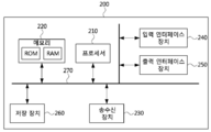
도 2는 발명의 제1 실시예에 따른 무선 통신 시스템에서 통신 노드의 구조를 도시한 개념도이다.
도 3은 본 발명의 제1 실시예에 따른 무선 통신 시스템에서 송신기 및 수신기를 도시한 개념도이다.
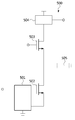
도 4는 본 발명의 제1 실시예에 따른 송수신 장치의 증폭기의 구조를 도시한 회로도이다.
도 5는 본 발명의 제1 실시예에 따른 따른 증폭기의 구조 및 기생 캐패시턴스 성분을 도시한 회로도이다.
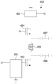
도 6a 및 도 6b는 본 발명의 제2 실시예에 따른 증폭기의 구조를 도시한 회로도이다.
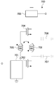
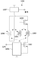
도 7은 본 발명의 제3 실시예에 따른 증폭기의 구조를 도시한 회로도이다.
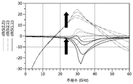
도 8은 본 발명의 제3 실시예에 따른 증폭기의 제2 인덕터에 입력되는 신호의 주파수 크기에 따른 산란(scattering)-파라미터(S-parameter)의 변화를 도시한 그래프이다.
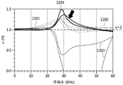
도 9는 본 발명의 제3 실시예에 따른 증폭기의 제2 인덕터에 입력되는 신호의 주파수 크기에 따른 안정 팩터(stability factor)를 도시한 그래프이다.
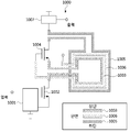
도 10a 및 도 10b는 본 발명의 제4 실시예에 따른 증폭기의 구조를 도시한 회로도이다.
도 11은 본 발명의 제1 내지 제4 실시예에 따른 증폭기들의 최대 가능 이득(maximum available gain; MAG) 그래프이다.
도 12는 본 발명의 제1 내지 제4 실시예에 따른 증폭기들의 안정 팩터(stability factor) 그래프이다.
도 13은 본 발명의 제1 내지 제4 실시예에 따른 증폭기들의 최소 잡음 지수(minimum noise figure) 그래프이다.
Claims (18)
- 증폭기(amplifier)에 있어서,
제1 및 제2 정합 망(matching network);
제1 및 제2 트랜지스터(transistor); 및
제1 내지 제3 인덕터(inductor)를 포함하는 변압기(transformer);를 포함하고,
상기 제1 트랜지스터의 게이트(gate) 및 소스(source)는 상기 제1 정합 망과 연결되고,
상기 제1 인덕터의 일단은 상기 제1 트랜지스터의 드레인(drain)과 연결되고, 상기 제1 인덕터의 타단은 상기 제2 트랜지스터의 소스와 연결되고,
상기 제2 인덕터의 일단은 상기 제2 트랜지스터의 게이트와 연결되고, 상기 제2 인덕터의 타단은 접지되고, 그리고
상기 제3 인덕터의 일단은 상기 제2 트랜지스터의 드레인과 연결되고, 상기 제3 인덕터의 타단은 상기 제2 정합 망과 연결되는, 증폭기. - 청구항 1에 있어서,
상기 변압기는 제1 내지 제3 층을 포함하고,
상기 제1 인덕터는 상기 제1 층에 배치되고,
상기 제2 인덕터는 상기 제2 층에 배치되고,
상기 제3 인덕터는 상기 제3 층에 배치되는, 증폭기. - 청구항 1에 있어서,
상기 제2 인덕터는 상기 제1 인덕터의 외곽을 둘러싸도록 배치되고,
상기 제3 인덕터는 상기 상기 제2 인덕터의 외곽을 둘러싸도록 배치되는, 증폭기. - 청구항 1에 있어서,
상기 제1 정합 망은 제1 입력단을 통해 입력되는 전기 신호를 상기 제1 트랜지스터의 게이트로 출력하고,
상기 제1 트랜지스터는 상기 전기 신호를 상기 드레인을 통해 상기 제1 인덕터로 출력하는, 증폭기. - 청구항 1에 있어서,
상기 제1 인덕터는 전기 신호에 따라 제1 자속(magnetic flux)을 형성하고,
상기 제2 인덕터는 상기 제1 자속에 의한 제2 자속을 형성하고,
상기 제2 자속의 방향은 상기 제1 자속의 방향과 반대인, 증폭기. - 청구항 1에 있어서,
상기 제2 트랜지스터는 상기 제1 인덕터에 의해 형성되는 제1 자속에 의해 소스 및 게이트에 전압을 형성하고,
상기 제2 트랜지스터의 소스 및 게이트 각각의 전압의 위상의 차이는 180도인, 증폭기. - 청구항 1에 있어서,
상기 제3 인덕터는 상기 제2 인덕터에 의해 형성되는 제2 자속에 의한 제3 자속을 형성하고,
상기 제3 자속의 방향은 상기 제2 자속의 방향과 동일한, 증폭기. - 청구항 1에 있어서,
상기 제1 내지 제3 인덕터는 전자기(electo-magnetic)적으로 커플링(coupling)되는, 증폭기. - 통신 노드에 있어서,
안테나; 및
상기 안테나와 연결되는 증폭기(amplifier);를 포함하고,
상기 증폭기는,
제1 및 제2 정합 망(matching network);
제1 및 제2 트랜지스터(transistor); 및
제1 내지 제3 인덕터(inductor)를 포함하는 변압기(transformer);를 포함하고,
상기 제1 트랜지스터의 게이트(gate) 및 소스(source)는 상기 제1 정합 망과 연결되고,
상기 제1 인덕터의 일단은 상기 제1 트랜지스터의 드레인(drain)과 연결되고, 상기 제1 인덕터의 타단은 상기 제2 트랜지스터의 소스와 연결되고,
상기 제2 인덕터의 일단은 상기 제2 트랜지스터의 게이트와 연결되고, 상기 제2 인덕터의 타단은 접지되고, 그리고
상기 제3 인덕터의 일단은 상기 제2 트랜지스터의 드레인과 연결되고, 상기 제3 인덕터의 타단은 상기 제2 정합 망과 연결되는, 통신 노드. - 청구항 9에 있어서,
상기 변압기는 제1 내지 제3 층을 포함하고,
상기 제1 인덕터는 상기 제1 층에 배치되고,
상기 제2 인덕터는 상기 제2 층에 배치되고,
상기 제3 인덕터는 상기 제3 층에 배치되는, 통신 노드. - 청구항 9에 있어서,
상기 제2 인덕터는 상기 제1 인덕터의 외곽을 둘러싸도록 배치되고,
상기 제3 인덕터는 상기 상기 제2 인덕터의 외곽을 둘러싸도록 배치되는, 통신 노드. - 청구항 9에 있어서,
상기 제1 정합 망은 제1 입력단을 통해 입력되는 전기 신호를 상기 제1 트랜지스터의 게이트로 출력하고,
상기 제1 트랜지스터는 상기 전기 신호를 상기 드레인을 통해 상기 제1 인덕터로 출력하는, 통신 노드. - 청구항 9에 있어서,
상기 제1 인덕터는 전기 신호에 따라 제1 자속(magnetic flux)을 형성하고,
상기 제2 인덕터는 상기 제1 자속에 의한 제2 자속을 형성하고,
상기 제2 자속의 방향은 상기 제1 자속의 방향과 반대인, 통신 노드. - 청구항 9에 있어서,
상기 제2 트랜지스터는 상기 제1 인덕터에 의해 형성되는 제1 자속에 의해 소스 및 게이트에 전압을 형성하고,
상기 제2 트랜지스터의 소스 및 게이트 각각의 전압의 위상의 차이는 180도인, 통신 노드. - 청구항 9에 있어서,
상기 제3 인덕터는 상기 제2 인덕터에 의해 형성되는 제2 자속에 의한 제3 자속을 형성하고,
상기 제3 자속의 방향은 상기 제2 자속의 방향과 동일한, 통신 노드. - 청구항 9에 있어서,
상기 제1 내지 제3 인덕터는 전자기(electo-magnetic)적으로 커플링(coupling)되는, 통신 노드. - 청구항 9에 있어서,
상기 통신 노드는 송신 신호 처리기;를 더 포함하고,
상기 증폭기는 상기 송신 신호 처리기로부터 출력되는 전송 신호를 증폭하고,
상기 안테나는 상기 증폭된 전송 신호를 방사하는, 통신 노드. - 청구항 9에 있어서,
상기 통신 노드는 수신 신호 처리기;를 더 포함하고,
상기 안테나는 수신 신호를 수신하고,
상기 증폭기는 상기 수신된 신호를 증폭하고,
상기 수신 신호 처리기는 상기 증폭된 신호를 처리하는, 통신 노드.
Priority Applications (2)
| Application Number | Priority Date | Filing Date | Title |
|---|---|---|---|
| KR1020190017587A KR102657358B1 (ko) | 2019-02-15 | 2019-02-15 | 변압기를 이용하여 전류를 재사용하기 위한 증폭기 및 그의 동작 방법 |
| US16/788,177 US11205998B2 (en) | 2019-02-15 | 2020-02-11 | Amplifier for reusing current by using transformer and method thereof |
Applications Claiming Priority (1)
| Application Number | Priority Date | Filing Date | Title |
|---|---|---|---|
| KR1020190017587A KR102657358B1 (ko) | 2019-02-15 | 2019-02-15 | 변압기를 이용하여 전류를 재사용하기 위한 증폭기 및 그의 동작 방법 |
Publications (2)
| Publication Number | Publication Date |
|---|---|
| KR20200099690A true KR20200099690A (ko) | 2020-08-25 |
| KR102657358B1 KR102657358B1 (ko) | 2024-04-15 |
Family
ID=72043708
Family Applications (1)
| Application Number | Title | Priority Date | Filing Date |
|---|---|---|---|
| KR1020190017587A Active KR102657358B1 (ko) | 2019-02-15 | 2019-02-15 | 변압기를 이용하여 전류를 재사용하기 위한 증폭기 및 그의 동작 방법 |
Country Status (2)
| Country | Link |
|---|---|
| US (1) | US11205998B2 (ko) |
| KR (1) | KR102657358B1 (ko) |
Families Citing this family (9)
| Publication number | Priority date | Publication date | Assignee | Title |
|---|---|---|---|---|
| FI3719993T3 (fi) | 2019-04-02 | 2023-03-20 | QuantalRF AG | Radiotaajuustehovahvistinjärjestelmä ja menetelmä sen lähtösignaalin linearisoimiseksi |
| US11356068B2 (en) * | 2020-07-14 | 2022-06-07 | Psemi Corporation | Two-stage LNA with mutual coupling |
| US12149210B2 (en) * | 2020-09-28 | 2024-11-19 | QuantalRF AG | Amplifier linearization using magnetically coupled feedback |
| US12149216B2 (en) | 2021-02-09 | 2024-11-19 | QuantalRF AG | System and method for adjusting amplifier bias using envelope tracking |
| WO2022173862A1 (en) | 2021-02-09 | 2022-08-18 | QuantalRF AG | System and method for adjusting amplifier bias current based on input signal envelope tracking |
| US11888453B2 (en) * | 2021-03-23 | 2024-01-30 | Qualcomm Incorporated | Wideband low-noise amplifier |
| EP4708678A3 (en) | 2021-04-02 | 2026-04-22 | Sehat Sutardja | Low noise amplifier incorporating sutardja transformer |
| US12519456B2 (en) | 2022-08-31 | 2026-01-06 | QuantalRF AG | Integrated coupled resonator filtering |
| US20240429962A1 (en) * | 2023-06-26 | 2024-12-26 | Apple Inc. | Gate-to-cascode coupled inductor-based lna for noise reduction and neutralization |
Citations (2)
| Publication number | Priority date | Publication date | Assignee | Title |
|---|---|---|---|---|
| JP2012257070A (ja) * | 2011-06-09 | 2012-12-27 | Nippon Telegr & Teleph Corp <Ntt> | トランスインピーダンスアンプ |
| KR20170119387A (ko) * | 2016-04-19 | 2017-10-27 | 한국전자통신연구원 | 저전력 고주파 증폭기 |
Family Cites Families (9)
| Publication number | Priority date | Publication date | Assignee | Title |
|---|---|---|---|---|
| CA2417395A1 (en) | 2002-01-28 | 2003-07-28 | James William Haslett | Monolithic transformer compensated circuit |
| KR100952424B1 (ko) | 2008-02-21 | 2010-04-14 | 한국전자통신연구원 | 트랜스포머의 커플링을 이용한 차동 전압 제어 발진기 및직교 전압 제어 발진기 |
| US8125276B2 (en) | 2010-03-12 | 2012-02-28 | Samsung Electro-Mechanics | Sharing of inductor interstage matching in parallel amplification system for wireless communication systems |
| US8792836B2 (en) | 2010-06-03 | 2014-07-29 | Broadcom Corporation | Front end module with compensating duplexer |
| US9306502B2 (en) | 2011-05-09 | 2016-04-05 | Qualcomm Incorporated | System providing switchable impedance transformer matching for power amplifiers |
| ITMI20111632A1 (it) * | 2011-09-09 | 2013-03-10 | St Microelectronics Srl | Dispositivo elettronico a riuso di corrente basato su componenti ad accoppiamento magnetico |
| US9831832B2 (en) | 2015-04-30 | 2017-11-28 | Taiwan Semiconductor Manufacturing Company, Ltd. | Low noise amplifier having transformer feedback and method of using the same |
| US9712195B2 (en) | 2015-05-13 | 2017-07-18 | Qualcomm Incorporated | Radio frequency low noise amplifier with on-chip matching and built-in tunable filter |
| KR101924639B1 (ko) | 2016-04-14 | 2018-12-03 | 한국전자통신연구원 | 고주파를 이용하여 무선 신호를 증폭하기 위한 회로 |
-
2019
- 2019-02-15 KR KR1020190017587A patent/KR102657358B1/ko active Active
-
2020
- 2020-02-11 US US16/788,177 patent/US11205998B2/en active Active
Patent Citations (2)
| Publication number | Priority date | Publication date | Assignee | Title |
|---|---|---|---|---|
| JP2012257070A (ja) * | 2011-06-09 | 2012-12-27 | Nippon Telegr & Teleph Corp <Ntt> | トランスインピーダンスアンプ |
| KR20170119387A (ko) * | 2016-04-19 | 2017-10-27 | 한국전자통신연구원 | 저전력 고주파 증폭기 |
Also Published As
| Publication number | Publication date |
|---|---|
| KR102657358B1 (ko) | 2024-04-15 |
| US20200266775A1 (en) | 2020-08-20 |
| US11205998B2 (en) | 2021-12-21 |
Similar Documents
| Publication | Publication Date | Title |
|---|---|---|
| KR102657358B1 (ko) | 변압기를 이용하여 전류를 재사용하기 위한 증폭기 및 그의 동작 방법 | |
| US10812023B2 (en) | Using multiple envelope tracking signals in a power amplifier | |
| KR102105130B1 (ko) | 고조파 정합을 위한 방법 및 장치 | |
| US8912846B2 (en) | Doherty amplifier arrangement | |
| JP6110034B2 (ja) | 構成可能な相互結合ソースディジェネレーションインダクタを持つ増幅器 | |
| EP3221963B1 (en) | Power amplifier for amplifying radio frequency signal | |
| CN108702134B (zh) | 负载调制放大器 | |
| JP6707642B2 (ja) | 電力増幅装置、エンベロープ追跡型の増幅装置、および信号を増幅する方法 | |
| CN105103442B (zh) | 具有经助推或经制推的源极退化电感的放大器 | |
| US11271527B2 (en) | Broadband harmonic load modulation doherty amplifiers | |
| CN106849879B (zh) | 功率放大器电路 | |
| US20160373144A1 (en) | Power amplification module | |
| US10389316B1 (en) | Apparatus and methods for power efficient CMOS and BiCMOS transmitters suitable for wireless applications | |
| KR101768361B1 (ko) | 트랜스포머를 이용하여 이득을 증가시키는 rf 증폭기 | |
| US20120235749A1 (en) | Doherty amplifier | |
| WO2023273417A1 (zh) | 射频功率放大电路、芯片及通信设备 | |
| CN111543005A (zh) | 功率放大器和包括功率放大器的射频设备 | |
| US8692620B2 (en) | Power amplifier | |
| US9509262B2 (en) | Concurrent multi-band radio frequency amplifying circuit | |
| KR102095867B1 (ko) | 음성 피드백 루프를 포함하는 저전력, 저잡음 증폭기 | |
| JP5983968B2 (ja) | 電力増幅回路及び電力増幅モジュール | |
| KR102527402B1 (ko) | 무선 통신 시스템에서 신호의 송수신을 스위칭하기 위한 장치 및 방법 | |
| KR20200114621A (ko) | 무선 통신 시스템에서 전력 증폭기 및 그의 동작 방법 | |
| US9479119B2 (en) | Amplifier circuit and operation method thereof | |
| CN120811298A (zh) | 一种射频放大器 |
Legal Events
| Date | Code | Title | Description |
|---|---|---|---|
| PA0109 | Patent application |
Patent event code: PA01091R01D Comment text: Patent Application Patent event date: 20190215 |
|
| PG1501 | Laying open of application | ||
| A201 | Request for examination | ||
| PA0201 | Request for examination |
Patent event code: PA02012R01D Patent event date: 20211006 Comment text: Request for Examination of Application Patent event code: PA02011R01I Patent event date: 20190215 Comment text: Patent Application |
|
| E902 | Notification of reason for refusal | ||
| PE0902 | Notice of grounds for rejection |
Comment text: Notification of reason for refusal Patent event date: 20230717 Patent event code: PE09021S01D |
|
| E701 | Decision to grant or registration of patent right | ||
| PE0701 | Decision of registration |
Patent event code: PE07011S01D Comment text: Decision to Grant Registration Patent event date: 20240125 |
|
| GRNT | Written decision to grant | ||
| PR0701 | Registration of establishment |
Comment text: Registration of Establishment Patent event date: 20240409 Patent event code: PR07011E01D |
|
| PR1002 | Payment of registration fee |
Payment date: 20240409 End annual number: 3 Start annual number: 1 |
|
| PG1601 | Publication of registration |