KR20200099696A - 인쇄회로기판 어셈블리 - Google Patents
인쇄회로기판 어셈블리 Download PDFInfo
- Publication number
- KR20200099696A KR20200099696A KR1020190017597A KR20190017597A KR20200099696A KR 20200099696 A KR20200099696 A KR 20200099696A KR 1020190017597 A KR1020190017597 A KR 1020190017597A KR 20190017597 A KR20190017597 A KR 20190017597A KR 20200099696 A KR20200099696 A KR 20200099696A
- Authority
- KR
- South Korea
- Prior art keywords
- circuit board
- printed circuit
- bus bar
- shield
- sensor
- Prior art date
- Legal status (The legal status is an assumption and is not a legal conclusion. Google has not performed a legal analysis and makes no representation as to the accuracy of the status listed.)
- Granted
Links
Images






Classifications
-
- H—ELECTRICITY
- H05—ELECTRIC TECHNIQUES NOT OTHERWISE PROVIDED FOR
- H05K—PRINTED CIRCUITS; CASINGS OR CONSTRUCTIONAL DETAILS OF ELECTRIC APPARATUS; MANUFACTURE OF ASSEMBLAGES OF ELECTRICAL COMPONENTS
- H05K1/00—Printed circuits
- H05K1/18—Printed circuits structurally associated with non-printed electric components
- H05K1/182—Printed circuits structurally associated with non-printed electric components associated with components mounted in printed circuit boards [PCB], e.g. insert-mounted components [IMC]
-
- G—PHYSICS
- G01—MEASURING; TESTING
- G01R—MEASURING ELECTRIC VARIABLES; MEASURING MAGNETIC VARIABLES
- G01R33/00—Arrangements or instruments for measuring magnetic variables
- G01R33/02—Measuring direction or magnitude of magnetic fields or magnetic flux
- G01R33/06—Measuring direction or magnitude of magnetic fields or magnetic flux using galvano-magnetic devices
-
- H—ELECTRICITY
- H05—ELECTRIC TECHNIQUES NOT OTHERWISE PROVIDED FOR
- H05K—PRINTED CIRCUITS; CASINGS OR CONSTRUCTIONAL DETAILS OF ELECTRIC APPARATUS; MANUFACTURE OF ASSEMBLAGES OF ELECTRICAL COMPONENTS
- H05K2201/00—Indexing scheme relating to printed circuits covered by H05K1/00
- H05K2201/10—Details of components or other objects attached to or integrated in a printed circuit board
- H05K2201/10007—Types of components
- H05K2201/10151—Sensor
-
- H—ELECTRICITY
- H05—ELECTRIC TECHNIQUES NOT OTHERWISE PROVIDED FOR
- H05K—PRINTED CIRCUITS; CASINGS OR CONSTRUCTIONAL DETAILS OF ELECTRIC APPARATUS; MANUFACTURE OF ASSEMBLAGES OF ELECTRICAL COMPONENTS
- H05K2201/00—Indexing scheme relating to printed circuits covered by H05K1/00
- H05K2201/10—Details of components or other objects attached to or integrated in a printed circuit board
- H05K2201/10227—Other objects, e.g. metallic pieces
- H05K2201/10272—Busbars, i.e. thick metal bars mounted on the printed circuit board [PCB] as high-current conductors
Landscapes
- Physics & Mathematics (AREA)
- Engineering & Computer Science (AREA)
- Microelectronics & Electronic Packaging (AREA)
- Condensed Matter Physics & Semiconductors (AREA)
- General Physics & Mathematics (AREA)
- Structure Of Printed Boards (AREA)
- Shielding Devices Or Components To Electric Or Magnetic Fields (AREA)
Abstract
Description
도 2는 본 발명의 일 실시 예에 따른, 인쇄회로기판 어셈블리의 일측 방향 사시도이다.
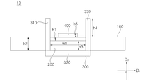
도 3a 및 3b는 본 발명의 다양한 실시 예에 따른, 인쇄회로기판 어셈블리의 정면 단면도이다.
도 4a 및 4b는 본 발명의 다양한 실시 예에 따른, 인쇄회로기판 어셈블리의 정면 단면도이다.
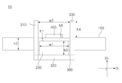
도 5a 및 5b는 본 발명의 다양한 실시 예에 따른, 인쇄회로기판 어셈블리의 측면 단면도이다.
110a, 110b: 관통 홀
200: 버스 바
300: 쉴드
310: 제1 세로부
320: 가로부
330: 제2 세로부
400: 센서
Claims (10)
- 인쇄회로기판;
상기 인쇄회로기판의 일면에 실장되고, 자기장을 감지하는 센서; 및
상기 인쇄회로기판의 타면에 접하여 배치되는 버스 바를 포함하고,
상기 인쇄회로기판의 타면 중 상기 버스 바에 접하는 부분과 상기 인쇄회로기판의 일면 사이의 두께는, 상기 인쇄회로기판의 타면 중 상기 버스 바에 접하는 부분을 제외한 나머지 부분과 상기 인쇄회로기판의 일면 사이의 두께보다 얇은 것을 특징으로 하는 인쇄회로기판 어셈블리. - 제1항에 있어서,
상기 버스 바는,
접착 및 열 프레스 중 적어도 하나에 기초하여, 상기 인쇄회로기판의 타면에 부착되는 것을 특징으로 하는 인쇄회로기판 어셈블리. - 제2항에 있어서,
상기 인쇄회로기판은,
상기 버스 바에 접하는 부분과 상기 일면 사이에 적어도 하나의 절연층을 구비하는 것을 특징으로 하는 인쇄회로기판 어셈블리. - 제3항에 있어서,
상기 센서는,
상기 버스 바를 통해 흐르는 전류에 의해 유도되는 자기장을 감지하여, 상기 버스 바에 흐르는 전류를 검출하는 홀 센서(hall sensor)인 것을 특징으로 하는 인쇄회로기판 어셈블리. - 제1항에 있어서,
상기 버스 바의 적어도 일부를 감싸도록 배치되는 쉴드를 더 포함하는 것을 특징으로 하는 인쇄회로기판 어셈블리. - 제5항에 있어서,
상기 쉴드는,
제1 세로부;
상기 제1 세로부로부터 구부러져 연장되는 가로부; 및
상기 가로부로부터 구부러져 연장되고, 상기 제1 세로부와 마주보는 제2 세로부를 포함하는 것을 특징으로 하는 인쇄회로기판 어셈블리. - 제6항에 있어서,
상기 인쇄회로기판은,
상기 인쇄회로기판의 일면에서 타면까지 관통되는 복수의 관통 홀을 구비하고,
상기 제1 세로부 및 상기 제2 세로부는,
상기 인쇄회로기판의 타면에서 일면으로 향하는 방향으로 상기 복수의 관통 홀에 각각 삽입되어, 일부분이 상기 인쇄회로기판의 일면에 노출되는 것을 특징으로 하는 인쇄회로기판 어셈블리. - 제7항에 있어서,
상기 인쇄회로기판의 일면에 노출되는, 상기 제1 세로부의 일부분 및 상기 제2 세로부의 일부분의 높이는, 상기 센서의 높이 이상인 것을 특징으로 하는 인쇄회로기판 어셈블리. - 제8항에 있어서,
상기 센서는,
상기 인쇄회로기판의 일면에 노출되는, 상기 제1 세로부의 일부분과 상기 제2 세로부의 일부분 사이에 배치되는 것을 특징으로 하는 인쇄회로기판 어셈블리. - 제9항에 있어서,
상기 제1 세로부 및 상기 제2 세로부의 너비는, 상기 센서의 너비 이상인 것을 특징으로 하는 인쇄회로기판 어셈블리.
Priority Applications (3)
| Application Number | Priority Date | Filing Date | Title |
|---|---|---|---|
| KR1020190017597A KR102699614B1 (ko) | 2019-02-15 | 2019-02-15 | 인쇄회로기판 어셈블리 |
| EP20157409.2A EP3696556A3 (en) | 2019-02-15 | 2020-02-14 | Printed circuit board assembly |
| US16/791,897 US11464113B2 (en) | 2019-02-15 | 2020-02-14 | Printed circuit board assembly |
Applications Claiming Priority (1)
| Application Number | Priority Date | Filing Date | Title |
|---|---|---|---|
| KR1020190017597A KR102699614B1 (ko) | 2019-02-15 | 2019-02-15 | 인쇄회로기판 어셈블리 |
Publications (2)
| Publication Number | Publication Date |
|---|---|
| KR20200099696A true KR20200099696A (ko) | 2020-08-25 |
| KR102699614B1 KR102699614B1 (ko) | 2024-08-27 |
Family
ID=72242226
Family Applications (1)
| Application Number | Title | Priority Date | Filing Date |
|---|---|---|---|
| KR1020190017597A Active KR102699614B1 (ko) | 2019-02-15 | 2019-02-15 | 인쇄회로기판 어셈블리 |
Country Status (1)
| Country | Link |
|---|---|
| KR (1) | KR102699614B1 (ko) |
Cited By (2)
| Publication number | Priority date | Publication date | Assignee | Title |
|---|---|---|---|---|
| WO2022270988A1 (ko) * | 2021-06-24 | 2022-12-29 | 삼성전자 주식회사 | 전자 부품의 배치 위치를 가이드하기 위한 구조를 포함하는 전자 장치 |
| US12213242B2 (en) | 2021-06-24 | 2025-01-28 | Samsung Electronics Co., Ltd. | Electronic device including a structure for guiding an arrangement position of an electronic component |
Citations (3)
| Publication number | Priority date | Publication date | Assignee | Title |
|---|---|---|---|---|
| KR20100029390A (ko) * | 2008-09-08 | 2010-03-17 | 현대자동차주식회사 | 하이브리드 차량용 인버터의 전류측정장치 |
| KR101398219B1 (ko) * | 2014-03-27 | 2014-05-22 | 태성전장주식회사 | 홀 센서를 이용한 대전류 측정장치 |
| KR101497836B1 (ko) * | 2013-10-22 | 2015-03-02 | 대성전기공업 주식회사 | 전류 감지 유니트 |
-
2019
- 2019-02-15 KR KR1020190017597A patent/KR102699614B1/ko active Active
Patent Citations (3)
| Publication number | Priority date | Publication date | Assignee | Title |
|---|---|---|---|---|
| KR20100029390A (ko) * | 2008-09-08 | 2010-03-17 | 현대자동차주식회사 | 하이브리드 차량용 인버터의 전류측정장치 |
| KR101497836B1 (ko) * | 2013-10-22 | 2015-03-02 | 대성전기공업 주식회사 | 전류 감지 유니트 |
| KR101398219B1 (ko) * | 2014-03-27 | 2014-05-22 | 태성전장주식회사 | 홀 센서를 이용한 대전류 측정장치 |
Cited By (2)
| Publication number | Priority date | Publication date | Assignee | Title |
|---|---|---|---|---|
| WO2022270988A1 (ko) * | 2021-06-24 | 2022-12-29 | 삼성전자 주식회사 | 전자 부품의 배치 위치를 가이드하기 위한 구조를 포함하는 전자 장치 |
| US12213242B2 (en) | 2021-06-24 | 2025-01-28 | Samsung Electronics Co., Ltd. | Electronic device including a structure for guiding an arrangement position of an electronic component |
Also Published As
| Publication number | Publication date |
|---|---|
| KR102699614B1 (ko) | 2024-08-27 |
Similar Documents
| Publication | Publication Date | Title |
|---|---|---|
| US11464113B2 (en) | Printed circuit board assembly | |
| US9557352B2 (en) | Current detection structure | |
| JP5985257B2 (ja) | 電流センサ | |
| US10335955B2 (en) | Proximity sensor arrangement | |
| JP6512061B2 (ja) | 電流センサ | |
| JP2020128960A (ja) | 電流センサ | |
| JP2020128961A (ja) | 電流センサ | |
| KR20200099696A (ko) | 인쇄회로기판 어셈블리 | |
| WO2016190087A1 (ja) | 電流センサ | |
| JPWO2022158158A5 (ko) | ||
| JP2011007596A (ja) | 電流センサ | |
| JP7489498B2 (ja) | 電流検出装置 | |
| KR101581175B1 (ko) | 전기 회로 장치 | |
| KR102350939B1 (ko) | 인쇄회로기판 어셈블리 | |
| WO2014046246A1 (ja) | シャント抵抗式電流センサ | |
| WO2021241586A1 (ja) | 電流センサ | |
| US7827865B2 (en) | Semiconductor acceleration sensor | |
| JP6058869B1 (ja) | 磁気センサ装置 | |
| JP6671978B2 (ja) | 電流センサ及び電流検出装置 | |
| JP6494895B1 (ja) | 磁気センサ装置 | |
| JP6994423B2 (ja) | 電装ユニット | |
| JP2018017651A (ja) | 電流センサモジュール | |
| JP6396794B2 (ja) | 磁気ラインセンサにおける磁石の位置決め方法及び位置決め装置 | |
| US11156642B2 (en) | Current detection apparatus | |
| CN107888047A (zh) | 直线电动机用磁体组件 |
Legal Events
| Date | Code | Title | Description |
|---|---|---|---|
| PA0109 | Patent application |
St.27 status event code: A-0-1-A10-A12-nap-PA0109 |
|
| PN2301 | Change of applicant |
St.27 status event code: A-3-3-R10-R13-asn-PN2301 St.27 status event code: A-3-3-R10-R11-asn-PN2301 |
|
| PG1501 | Laying open of application |
St.27 status event code: A-1-1-Q10-Q12-nap-PG1501 |
|
| N231 | Notification of change of applicant | ||
| PN2301 | Change of applicant |
St.27 status event code: A-3-3-R10-R13-asn-PN2301 St.27 status event code: A-3-3-R10-R11-asn-PN2301 |
|
| PN2301 | Change of applicant |
St.27 status event code: A-3-3-R10-R13-asn-PN2301 St.27 status event code: A-3-3-R10-R11-asn-PN2301 |
|
| A201 | Request for examination | ||
| PA0201 | Request for examination |
St.27 status event code: A-1-2-D10-D11-exm-PA0201 |
|
| D13-X000 | Search requested |
St.27 status event code: A-1-2-D10-D13-srh-X000 |
|
| D14-X000 | Search report completed |
St.27 status event code: A-1-2-D10-D14-srh-X000 |
|
| E902 | Notification of reason for refusal | ||
| PE0902 | Notice of grounds for rejection |
St.27 status event code: A-1-2-D10-D21-exm-PE0902 |
|
| P11-X000 | Amendment of application requested |
St.27 status event code: A-2-2-P10-P11-nap-X000 |
|
| P13-X000 | Application amended |
St.27 status event code: A-2-2-P10-P13-nap-X000 |
|
| E601 | Decision to refuse application | ||
| PE0601 | Decision on rejection of patent |
St.27 status event code: N-2-6-B10-B15-exm-PE0601 |
|
| P11-X000 | Amendment of application requested |
St.27 status event code: A-2-2-P10-P11-nap-X000 |
|
| P13-X000 | Application amended |
St.27 status event code: A-2-2-P10-P13-nap-X000 |
|
| PX0901 | Re-examination |
St.27 status event code: A-2-3-E10-E12-rex-PX0901 |
|
| P11-X000 | Amendment of application requested |
St.27 status event code: A-2-2-P10-P11-nap-X000 |
|
| P13-X000 | Application amended |
St.27 status event code: A-2-2-P10-P13-nap-X000 |
|
| PX0701 | Decision of registration after re-examination |
St.27 status event code: A-3-4-F10-F13-rex-PX0701 |
|
| X701 | Decision to grant (after re-examination) | ||
| GRNT | Written decision to grant | ||
| PR0701 | Registration of establishment |
St.27 status event code: A-2-4-F10-F11-exm-PR0701 |
|
| PR1002 | Payment of registration fee |
St.27 status event code: A-2-2-U10-U11-oth-PR1002 Fee payment year number: 1 |
|
| PG1601 | Publication of registration |
St.27 status event code: A-4-4-Q10-Q13-nap-PG1601 |