KR20200099954A - 복합 하전 입자 빔 장치, 및 제어 방법 - Google Patents
복합 하전 입자 빔 장치, 및 제어 방법 Download PDFInfo
- Publication number
- KR20200099954A KR20200099954A KR1020190137409A KR20190137409A KR20200099954A KR 20200099954 A KR20200099954 A KR 20200099954A KR 1020190137409 A KR1020190137409 A KR 1020190137409A KR 20190137409 A KR20190137409 A KR 20190137409A KR 20200099954 A KR20200099954 A KR 20200099954A
- Authority
- KR
- South Korea
- Prior art keywords
- ion beam
- unit
- voltage
- booster
- acceleration voltage
- Prior art date
- Legal status (The legal status is an assumption and is not a legal conclusion. Google has not performed a legal analysis and makes no representation as to the accuracy of the status listed.)
- Granted
Links
Images


Classifications
-
- H—ELECTRICITY
- H01—ELECTRIC ELEMENTS
- H01J—ELECTRIC DISCHARGE TUBES OR DISCHARGE LAMPS
- H01J37/00—Discharge tubes with provision for introducing objects or material to be exposed to the discharge, e.g. for the purpose of examination or processing thereof
- H01J37/02—Details
- H01J37/248—Components associated with high voltage supply
-
- H—ELECTRICITY
- H01—ELECTRIC ELEMENTS
- H01J—ELECTRIC DISCHARGE TUBES OR DISCHARGE LAMPS
- H01J37/00—Discharge tubes with provision for introducing objects or material to be exposed to the discharge, e.g. for the purpose of examination or processing thereof
- H01J37/30—Electron-beam or ion-beam tubes for localised treatment of objects
- H01J37/302—Controlling tubes by external information, e.g. program control
- H01J37/3023—Program control
-
- H—ELECTRICITY
- H01—ELECTRIC ELEMENTS
- H01J—ELECTRIC DISCHARGE TUBES OR DISCHARGE LAMPS
- H01J37/00—Discharge tubes with provision for introducing objects or material to be exposed to the discharge, e.g. for the purpose of examination or processing thereof
- H01J37/02—Details
- H01J37/24—Circuit arrangements not adapted to a particular application of the tube and not otherwise provided for
- H01J37/241—High voltage power supply or regulation circuits
-
- H—ELECTRICITY
- H01—ELECTRIC ELEMENTS
- H01J—ELECTRIC DISCHARGE TUBES OR DISCHARGE LAMPS
- H01J37/00—Discharge tubes with provision for introducing objects or material to be exposed to the discharge, e.g. for the purpose of examination or processing thereof
- H01J37/02—Details
- H01J37/04—Arrangements of electrodes and associated parts for generating or controlling the discharge, e.g. electron-optical arrangement or ion-optical arrangement
- H01J37/08—Ion sources; Ion guns
-
- H—ELECTRICITY
- H01—ELECTRIC ELEMENTS
- H01J—ELECTRIC DISCHARGE TUBES OR DISCHARGE LAMPS
- H01J37/00—Discharge tubes with provision for introducing objects or material to be exposed to the discharge, e.g. for the purpose of examination or processing thereof
- H01J37/02—Details
- H01J37/04—Arrangements of electrodes and associated parts for generating or controlling the discharge, e.g. electron-optical arrangement or ion-optical arrangement
- H01J37/147—Arrangements for directing or deflecting the discharge along a desired path
-
- H—ELECTRICITY
- H01—ELECTRIC ELEMENTS
- H01J—ELECTRIC DISCHARGE TUBES OR DISCHARGE LAMPS
- H01J37/00—Discharge tubes with provision for introducing objects or material to be exposed to the discharge, e.g. for the purpose of examination or processing thereof
- H01J37/02—Details
- H01J37/21—Means for adjusting the focus
-
- H—ELECTRICITY
- H01—ELECTRIC ELEMENTS
- H01J—ELECTRIC DISCHARGE TUBES OR DISCHARGE LAMPS
- H01J37/00—Discharge tubes with provision for introducing objects or material to be exposed to the discharge, e.g. for the purpose of examination or processing thereof
- H01J37/02—Details
- H01J37/24—Circuit arrangements not adapted to a particular application of the tube and not otherwise provided for
- H01J37/243—Beam current control or regulation circuits
-
- H—ELECTRICITY
- H01—ELECTRIC ELEMENTS
- H01J—ELECTRIC DISCHARGE TUBES OR DISCHARGE LAMPS
- H01J37/00—Discharge tubes with provision for introducing objects or material to be exposed to the discharge, e.g. for the purpose of examination or processing thereof
- H01J37/26—Electron or ion microscopes; Electron or ion diffraction tubes
- H01J37/28—Electron or ion microscopes; Electron or ion diffraction tubes with scanning beams
-
- H—ELECTRICITY
- H01—ELECTRIC ELEMENTS
- H01J—ELECTRIC DISCHARGE TUBES OR DISCHARGE LAMPS
- H01J37/00—Discharge tubes with provision for introducing objects or material to be exposed to the discharge, e.g. for the purpose of examination or processing thereof
- H01J37/30—Electron-beam or ion-beam tubes for localised treatment of objects
- H01J37/305—Electron-beam or ion-beam tubes for localised treatment of objects for casting, melting, evaporating, or etching
- H01J37/3053—Electron-beam or ion-beam tubes for localised treatment of objects for casting, melting, evaporating, or etching for evaporating or etching
- H01J37/3056—Electron-beam or ion-beam tubes for localised treatment of objects for casting, melting, evaporating, or etching for evaporating or etching for microworking, e. g. etching of gratings or trimming of electrical components
-
- H—ELECTRICITY
- H01—ELECTRIC ELEMENTS
- H01J—ELECTRIC DISCHARGE TUBES OR DISCHARGE LAMPS
- H01J2237/00—Discharge tubes exposing object to beam, e.g. for analysis treatment, etching, imaging
- H01J2237/04—Means for controlling the discharge
- H01J2237/047—Changing particle velocity
- H01J2237/0473—Changing particle velocity accelerating
-
- H—ELECTRICITY
- H01—ELECTRIC ELEMENTS
- H01J—ELECTRIC DISCHARGE TUBES OR DISCHARGE LAMPS
- H01J2237/00—Discharge tubes exposing object to beam, e.g. for analysis treatment, etching, imaging
- H01J2237/30—Electron or ion beam tubes for processing objects
- H01J2237/317—Processing objects on a microscale
- H01J2237/31749—Focused ion beam
Landscapes
- Chemical & Material Sciences (AREA)
- Analytical Chemistry (AREA)
- Physics & Mathematics (AREA)
- Engineering & Computer Science (AREA)
- Plasma & Fusion (AREA)
- Analysing Materials By The Use Of Radiation (AREA)
- Electron Sources, Ion Sources (AREA)
Abstract
복합 하전 입자 빔 장치는, 이온 빔을 공급하는 이온 공급부와, 이온 공급부가 공급하는 이온 빔에 가속 전압을 인가함으로써 가속시키는 가속 전압 인가부와, 이온 빔을 집속시키는 제1 집속부와, 이온 빔에 빔 부스터 전압을 인가하는 빔 부스터 전압 인가부와, 이온 빔을 집속시켜 시료에 조사시키는 제2 집속부와, 전자 빔을 시료에 조사하는 전자 빔 조사부와, 빔 부스터 전압 인가부가 이온 빔에 인가하는 빔 부스터 전압의 값을, 가속 전압 인가부가 이온 빔에 인가하는 가속 전압의 값과, 집속시킨 이온 빔의 초점 거리에 따라 미리 결정된 설정값에 의거하여 설정하는 제어부를 구비한다.
Description
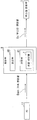
도 2는 본 발명의 실시 형태에 따른 주사계의 절연의 일례를 나타내는 도면이다.
도 3은 본 발명의 실시 형태에 따른 제어부의 구성의 일례를 나타내는 도면이다.
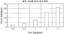
도 4는 본 발명의 실시 형태에 따른 가속 전압값에 대한 빔 부스터 전압값의 범위의 일례를 나타내는 도면이다.
도 5는 본 발명의 실시 형태에 따른 FIB 작동 거리와 SEM 작동 거리의 일례를 나타내는 도면이다.
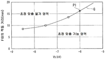
도 6은 본 발명의 실시 형태에 따른 FIB 작동 거리와 빔 부스터 전압의 관계의 일례를 나타내는 도면이다.
도 7은 본 발명의 실시 형태에 따른 빔 부스터 전압값의 설정 처리의 일례를 나타내는 도면이다.
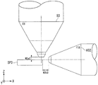
도 8은 본 발명의 실시 형태의 변형예에 따른 집속 이온 빔 경통, 및 전자 빔 경통의 배치의 제1 예를 나타내는 도면이다.
도 9는 본 발명의 실시 형태의 변형예에 따른 집속 이온 빔 경통, 및 전자 빔 경통의 배치의 제2 예를 나타내는 도면이다.
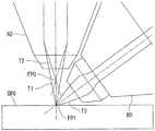
도 10은 종래의 복합 하전 입자 빔 장치에 있어서의 빔 궤도의 일례를 나타내는 도면이다.
D1 집속 이온 빔 장치
D2 주사형 전자 현미경
1 이온원 제어부
10 가속 전원
3 콘덴서 렌즈
4 빔 부스터
5 대물렌즈
9 제어부
91 기억부
T 전압 테이블
Eb 빔 부스터 전압값
TEb 빔 부스터 전압 설정값
Eacc 가속 전압값
Claims (4)
- 이온 빔을 공급하는 이온 공급부와,
상기 이온 공급부가 공급하는 상기 이온 빔에 가속 전압을 인가함으로써 가속시키는 가속 전압 인가부와,
상기 가속 전압 인가부가 가속시킨 상기 이온 빔을 집속시키는 제1 집속부와,
상기 제1 집속부가 집속시킨 상기 이온 빔에 빔 부스터 전압을 인가하는 빔 부스터 전압 인가부와,
상기 빔 부스터 전압 인가부가 상기 빔 부스터 전압을 인가한 상기 이온 빔을 집속시켜 시료에 조사시키는 제2 집속부와,
전자 빔을 상기 시료에 조사하는 전자 빔 조사부와,
상기 빔 부스터 전압 인가부가 상기 이온 빔에 인가하는 상기 빔 부스터 전압의 값을, 상기 가속 전압 인가부가 상기 이온 빔에 인가하는 상기 가속 전압의 값과, 집속시킨 상기 이온 빔의 초점 거리에 따라 미리 결정된 설정값에 의거하여 설정하는 제어부를 구비하는 복합 하전 입자 빔 장치. - 청구항 1에 있어서,
집속한 상기 이온 빔의 조사점 및 초점과, 상기 전자 빔의 조사점은 상기 시료 상의 동일한 점인 복합 하전 입자 빔 장치. - 청구항 1 또는 청구항 2에 있어서,
상기 제어부는, 상기 가속 전압의 값과 상기 설정값의 세트를 기억하는 기억부로부터 읽어 낸 상기 세트에 의거하여, 상기 빔 부스터 전압의 값을 상기 설정값으로 설정하는 복합 하전 입자 빔 장치. - 이온 빔을 공급하는 이온 공급부와,
상기 이온 공급부가 공급하는 상기 이온 빔에 가속 전압을 인가함으로써 가속시키는 가속 전압 인가부와,
상기 가속 전압 인가부가 가속시킨 상기 이온 빔을 집속시키는 제1 집속부와,
상기 제1 집속부가 집속시킨 상기 이온 빔에 빔 부스터 전압을 인가하는 빔 부스터 전압 인가부와,
상기 빔 부스터 전압 인가부가 상기 빔 부스터 전압을 인가한 상기 이온 빔을 집속시켜 시료에 조사시키는 제2 집속부와,
전자 빔을 상기 시료에 조사하는 전자 빔 조사부를 구비하는 복합 하전 입자 빔 장치에 있어서의 제어 방법에 있어서,
상기 빔 부스터 전압 인가부가 상기 이온 빔에 인가하는 상기 빔 부스터 전압의 값을, 상기 가속 전압 인가부가 상기 이온 빔에 인가하는 상기 가속 전압의 값과, 집속시킨 상기 이온 빔의 초점 거리에 따라 미리 결정된 설정값에 의거하여 설정하는 제어 과정을 갖는 제어 방법.
Applications Claiming Priority (2)
| Application Number | Priority Date | Filing Date | Title |
|---|---|---|---|
| JP2019025928A JP7154593B2 (ja) | 2019-02-15 | 2019-02-15 | 複合荷電粒子ビーム装置、及び制御方法 |
| JPJP-P-2019-025928 | 2019-02-15 |
Publications (2)
| Publication Number | Publication Date |
|---|---|
| KR20200099954A true KR20200099954A (ko) | 2020-08-25 |
| KR102713097B1 KR102713097B1 (ko) | 2024-10-04 |
Family
ID=72043678
Family Applications (1)
| Application Number | Title | Priority Date | Filing Date |
|---|---|---|---|
| KR1020190137409A Active KR102713097B1 (ko) | 2019-02-15 | 2019-10-31 | 복합 하전 입자 빔 장치, 및 제어 방법 |
Country Status (5)
| Country | Link |
|---|---|
| US (1) | US11017982B2 (ko) |
| JP (1) | JP7154593B2 (ko) |
| KR (1) | KR102713097B1 (ko) |
| CN (1) | CN111584335B (ko) |
| TW (1) | TWI841663B (ko) |
Families Citing this family (2)
| Publication number | Priority date | Publication date | Assignee | Title |
|---|---|---|---|---|
| EP4075476A1 (en) * | 2021-04-15 | 2022-10-19 | ASML Netherlands B.V. | Electron-optical device |
| CN114236364B (zh) * | 2022-02-24 | 2022-05-31 | 上海聚跃检测技术有限公司 | 一种集成电路芯片的失效分析方法及系统 |
Citations (10)
| Publication number | Priority date | Publication date | Assignee | Title |
|---|---|---|---|---|
| JPH10106474A (ja) | 1996-09-30 | 1998-04-24 | Seiko Instr Inc | イオンビームによる加工装置 |
| JPH11223588A (ja) | 1998-02-09 | 1999-08-17 | Hitachi Ltd | 透過形電子顕微鏡用薄片試料作製方法 |
| JP2000173520A (ja) | 1998-11-30 | 2000-06-23 | Advantest Corp | 粒子線装置 |
| JP2006236836A (ja) | 2005-02-25 | 2006-09-07 | Sii Nanotechnology Inc | 試料高さ調整方法と試料観察方法と試料加工方法および荷電粒子ビーム装置 |
| JP2007103108A (ja) | 2005-10-03 | 2007-04-19 | Sii Nanotechnology Inc | 集束イオンビームによる加工方法 |
| JP2007193977A (ja) | 2006-01-17 | 2007-08-02 | Hitachi High-Technologies Corp | 荷電ビーム装置及び荷電ビーム加工方法 |
| JP2009272293A (ja) | 2008-04-11 | 2009-11-19 | Hitachi High-Technologies Corp | 集束イオンビーム装置 |
| JP2013125583A (ja) * | 2011-12-13 | 2013-06-24 | Hitachi High-Technologies Corp | 走査電子線装置およびそれを用いた寸法計測方法 |
| JP2013196826A (ja) | 2012-03-16 | 2013-09-30 | Honda Motor Co Ltd | バッテリモジュール |
| JP2016146237A (ja) * | 2015-02-06 | 2016-08-12 | 株式会社日立ハイテクノロジーズ | 複合荷電粒子線装置 |
Family Cites Families (9)
| Publication number | Priority date | Publication date | Assignee | Title |
|---|---|---|---|---|
| EP1210723B1 (en) * | 2000-01-21 | 2009-03-18 | Fei Company | Shaped and low density focused ion beams |
| JP4789260B2 (ja) * | 2006-08-23 | 2011-10-12 | エスアイアイ・ナノテクノロジー株式会社 | 荷電粒子ビーム装置及びアパーチャの軸調整方法 |
| JP5044813B2 (ja) * | 2007-02-19 | 2012-10-10 | エスアイアイ・ナノテクノロジー株式会社 | 集束イオンビーム装置及び荷電粒子光学系の調整方法 |
| US8742361B2 (en) * | 2012-06-07 | 2014-06-03 | Fei Company | Focused charged particle column for operation at different beam energies at a target |
| US8933414B2 (en) | 2013-02-27 | 2015-01-13 | Fei Company | Focused ion beam low kV enhancement |
| US10410828B2 (en) * | 2014-12-22 | 2019-09-10 | Carl Zeiss Microscopy, Llc | Charged particle beam system and methods |
| JP6554288B2 (ja) * | 2015-01-26 | 2019-07-31 | 株式会社日立ハイテクノロジーズ | 荷電粒子線装置 |
| CN105668514B (zh) * | 2016-01-25 | 2019-04-23 | 北京航空航天大学 | 一种聚焦离子束-电子束双束融合可控微纳加工的方法 |
| JP6906786B2 (ja) * | 2017-03-27 | 2021-07-21 | 株式会社日立ハイテクサイエンス | 試料保持具、部材装着用器具、および荷電粒子ビーム装置 |
-
2019
- 2019-02-15 JP JP2019025928A patent/JP7154593B2/ja active Active
- 2019-10-31 KR KR1020190137409A patent/KR102713097B1/ko active Active
-
2020
- 2020-01-16 TW TW109101467A patent/TWI841663B/zh active
- 2020-01-20 CN CN202010064843.3A patent/CN111584335B/zh active Active
- 2020-02-07 US US16/785,362 patent/US11017982B2/en active Active
Patent Citations (10)
| Publication number | Priority date | Publication date | Assignee | Title |
|---|---|---|---|---|
| JPH10106474A (ja) | 1996-09-30 | 1998-04-24 | Seiko Instr Inc | イオンビームによる加工装置 |
| JPH11223588A (ja) | 1998-02-09 | 1999-08-17 | Hitachi Ltd | 透過形電子顕微鏡用薄片試料作製方法 |
| JP2000173520A (ja) | 1998-11-30 | 2000-06-23 | Advantest Corp | 粒子線装置 |
| JP2006236836A (ja) | 2005-02-25 | 2006-09-07 | Sii Nanotechnology Inc | 試料高さ調整方法と試料観察方法と試料加工方法および荷電粒子ビーム装置 |
| JP2007103108A (ja) | 2005-10-03 | 2007-04-19 | Sii Nanotechnology Inc | 集束イオンビームによる加工方法 |
| JP2007193977A (ja) | 2006-01-17 | 2007-08-02 | Hitachi High-Technologies Corp | 荷電ビーム装置及び荷電ビーム加工方法 |
| JP2009272293A (ja) | 2008-04-11 | 2009-11-19 | Hitachi High-Technologies Corp | 集束イオンビーム装置 |
| JP2013125583A (ja) * | 2011-12-13 | 2013-06-24 | Hitachi High-Technologies Corp | 走査電子線装置およびそれを用いた寸法計測方法 |
| JP2013196826A (ja) | 2012-03-16 | 2013-09-30 | Honda Motor Co Ltd | バッテリモジュール |
| JP2016146237A (ja) * | 2015-02-06 | 2016-08-12 | 株式会社日立ハイテクノロジーズ | 複合荷電粒子線装置 |
Non-Patent Citations (1)
| Title |
|---|
| Michael Rauscher and Erich Plies, 「Low Energy focused ion beam system design」, Journal of Vacuum Science & Technology A, American Vacuum Society, 2006, 24(4), p. 1055-1066 |
Also Published As
| Publication number | Publication date |
|---|---|
| TW202109598A (zh) | 2021-03-01 |
| CN111584335B (zh) | 2023-09-19 |
| JP2020136002A (ja) | 2020-08-31 |
| US20200266029A1 (en) | 2020-08-20 |
| US11017982B2 (en) | 2021-05-25 |
| JP7154593B2 (ja) | 2022-10-18 |
| TWI841663B (zh) | 2024-05-11 |
| KR102713097B1 (ko) | 2024-10-04 |
| CN111584335A (zh) | 2020-08-25 |
Similar Documents
| Publication | Publication Date | Title |
|---|---|---|
| JP5792509B2 (ja) | 荷電粒子ビーム装置及び試料加工方法 | |
| US6949756B2 (en) | Shaped and low density focused ion beams | |
| TWI803572B (zh) | 帶電粒子束裝置、試料加工觀察方法 | |
| US20140361165A1 (en) | Method for imaging a sample in a charged particle apparatus | |
| US10636615B2 (en) | Composite beam apparatus | |
| JPWO2019224895A1 (ja) | 荷電粒子線装置及びその軸調整方法 | |
| IL237738A (en) | Install a bi-lens electron beam device and high resolution imaging methods with high and low beam currents | |
| KR20180109687A (ko) | 하전 입자 빔 장치 | |
| KR102713097B1 (ko) | 복합 하전 입자 빔 장치, 및 제어 방법 | |
| US9761407B2 (en) | Ion beam device and emitter tip adjustment method | |
| KR102815204B1 (ko) | 하전 입자 빔 장치, 복합 하전 입자 빔 장치, 및 하전 입자 빔 장치의 제어 방법 | |
| WO2023032078A1 (ja) | 集束イオンビーム装置 | |
| JP7090902B2 (ja) | 集束イオンビーム装置及び集束イオンビーム装置の制御方法 | |
| US11257655B2 (en) | Focused ion beam apparatus, and control method for focused ion beam apparatus | |
| US8390152B2 (en) | Device and method for generating a stable high voltage | |
| JP7627791B2 (ja) | 荷電粒子線装置及び荷電粒子線装置におけるビームの偏向方法 | |
| JP2001351561A (ja) | 集束イオンビーム装置 | |
| WO2025203456A1 (ja) | 複合ビーム装置 |
Legal Events
| Date | Code | Title | Description |
|---|---|---|---|
| PA0109 | Patent application |
Patent event code: PA01091R01D Comment text: Patent Application Patent event date: 20191031 |
|
| PG1501 | Laying open of application | ||
| A201 | Request for examination | ||
| PA0201 | Request for examination |
Patent event code: PA02012R01D Patent event date: 20220822 Comment text: Request for Examination of Application Patent event code: PA02011R01I Patent event date: 20191031 Comment text: Patent Application |
|
| GRNT | Written decision to grant | ||
| PR0701 | Registration of establishment |
Comment text: Registration of Establishment Patent event date: 20240927 Patent event code: PR07011E01D |
|
| PR1002 | Payment of registration fee |
Payment date: 20240930 End annual number: 3 Start annual number: 1 |
|
| PG1601 | Publication of registration |