KR20220089618A - 측정 시스템 - Google Patents
측정 시스템 Download PDFInfo
- Publication number
- KR20220089618A KR20220089618A KR1020210149645A KR20210149645A KR20220089618A KR 20220089618 A KR20220089618 A KR 20220089618A KR 1020210149645 A KR1020210149645 A KR 1020210149645A KR 20210149645 A KR20210149645 A KR 20210149645A KR 20220089618 A KR20220089618 A KR 20220089618A
- Authority
- KR
- South Korea
- Prior art keywords
- optical
- probe
- measurement
- light
- measurement system
- Prior art date
- Legal status (The legal status is an assumption and is not a legal conclusion. Google has not performed a legal analysis and makes no representation as to the accuracy of the status listed.)
- Ceased
Links
Images


Classifications
-
- G—PHYSICS
- G01—MEASURING; TESTING
- G01R—MEASURING ELECTRIC VARIABLES; MEASURING MAGNETIC VARIABLES
- G01R31/00—Arrangements for testing electric properties; Arrangements for locating electric faults; Arrangements for electrical testing characterised by what is being tested not provided for elsewhere
- G01R31/26—Testing of individual semiconductor devices
- G01R31/2601—Apparatus or methods therefor
-
- G—PHYSICS
- G01—MEASURING; TESTING
- G01N—INVESTIGATING OR ANALYSING MATERIALS BY DETERMINING THEIR CHEMICAL OR PHYSICAL PROPERTIES
- G01N21/00—Investigating or analysing materials by the use of optical means, i.e. using sub-millimetre waves, infrared, visible or ultraviolet light
- G01N21/84—Systems specially adapted for particular applications
- G01N21/88—Investigating the presence of flaws or contamination
- G01N21/95—Investigating the presence of flaws or contamination characterised by the material or shape of the object to be examined
- G01N21/9501—Semiconductor wafers
-
- G—PHYSICS
- G01—MEASURING; TESTING
- G01R—MEASURING ELECTRIC VARIABLES; MEASURING MAGNETIC VARIABLES
- G01R1/00—Details of instruments or arrangements of the types included in groups G01R5/00 - G01R13/00 and G01R31/00
- G01R1/02—General constructional details
- G01R1/06—Measuring leads; Measuring probes
- G01R1/067—Measuring probes
- G01R1/07—Non contact-making probes
- G01R1/071—Non contact-making probes containing electro-optic elements
-
- G—PHYSICS
- G01—MEASURING; TESTING
- G01R—MEASURING ELECTRIC VARIABLES; MEASURING MAGNETIC VARIABLES
- G01R1/00—Details of instruments or arrangements of the types included in groups G01R5/00 - G01R13/00 and G01R31/00
- G01R1/02—General constructional details
- G01R1/06—Measuring leads; Measuring probes
- G01R1/067—Measuring probes
- G01R1/073—Multiple probes
- G01R1/07392—Multiple probes manipulating each probe element or tip individually
-
- G—PHYSICS
- G01—MEASURING; TESTING
- G01R—MEASURING ELECTRIC VARIABLES; MEASURING MAGNETIC VARIABLES
- G01R31/00—Arrangements for testing electric properties; Arrangements for locating electric faults; Arrangements for electrical testing characterised by what is being tested not provided for elsewhere
- G01R31/26—Testing of individual semiconductor devices
- G01R31/2607—Circuits therefor
- G01R31/2632—Circuits therefor for testing diodes
- G01R31/2635—Testing light-emitting diodes, laser diodes or photodiodes
-
- G—PHYSICS
- G01—MEASURING; TESTING
- G01R—MEASURING ELECTRIC VARIABLES; MEASURING MAGNETIC VARIABLES
- G01R31/00—Arrangements for testing electric properties; Arrangements for locating electric faults; Arrangements for electrical testing characterised by what is being tested not provided for elsewhere
- G01R31/26—Testing of individual semiconductor devices
- G01R31/265—Contactless testing
- G01R31/2656—Contactless testing using non-ionising electromagnetic radiation, e.g. optical radiation
-
- G—PHYSICS
- G02—OPTICS
- G02B—OPTICAL ELEMENTS, SYSTEMS OR APPARATUS
- G02B27/00—Optical systems or apparatus not provided for by any of the groups G02B1/00 - G02B26/00, G02B30/00
- G02B27/42—Diffraction optics, i.e. systems including a diffractive element being designed for providing a diffractive effect
-
- H01L31/042—
-
- H—ELECTRICITY
- H10—SEMICONDUCTOR DEVICES; ELECTRIC SOLID-STATE DEVICES NOT OTHERWISE PROVIDED FOR
- H10F—INORGANIC SEMICONDUCTOR DEVICES SENSITIVE TO INFRARED RADIATION, LIGHT, ELECTROMAGNETIC RADIATION OF SHORTER WAVELENGTH OR CORPUSCULAR RADIATION
- H10F19/00—Integrated devices, or assemblies of multiple devices, comprising at least one photovoltaic cell covered by group H10F10/00, e.g. photovoltaic modules
-
- H—ELECTRICITY
- H10—SEMICONDUCTOR DEVICES; ELECTRIC SOLID-STATE DEVICES NOT OTHERWISE PROVIDED FOR
- H10P—GENERIC PROCESSES OR APPARATUS FOR THE MANUFACTURE OR TREATMENT OF DEVICES COVERED BY CLASS H10
- H10P74/00—Testing or measuring during manufacture or treatment of wafers, substrates or devices
- H10P74/23—Testing or measuring during manufacture or treatment of wafers, substrates or devices characterised by multiple measurements, corrections, marking or sorting processes
- H10P74/235—Testing or measuring during manufacture or treatment of wafers, substrates or devices characterised by multiple measurements, corrections, marking or sorting processes comprising optical enhancement of defects or not-directly-visible states
-
- G—PHYSICS
- G01—MEASURING; TESTING
- G01N—INVESTIGATING OR ANALYSING MATERIALS BY DETERMINING THEIR CHEMICAL OR PHYSICAL PROPERTIES
- G01N21/00—Investigating or analysing materials by the use of optical means, i.e. using sub-millimetre waves, infrared, visible or ultraviolet light
- G01N21/62—Systems in which the material investigated is excited whereby it emits light or causes a change in wavelength of the incident light
- G01N21/66—Systems in which the material investigated is excited whereby it emits light or causes a change in wavelength of the incident light electrically excited, e.g. electroluminescence
-
- G—PHYSICS
- G01—MEASURING; TESTING
- G01R—MEASURING ELECTRIC VARIABLES; MEASURING MAGNETIC VARIABLES
- G01R1/00—Details of instruments or arrangements of the types included in groups G01R5/00 - G01R13/00 and G01R31/00
- G01R1/02—General constructional details
- G01R1/04—Housings; Supporting members; Arrangements of terminals
- G01R1/0408—Test fixtures or contact fields; Connectors or connecting adaptors; Test clips; Test sockets
- G01R1/0491—Test fixtures or contact fields; Connectors or connecting adaptors; Test clips; Test sockets for testing integrated circuits on wafers, e.g. wafer-level test cartridge
Landscapes
- Physics & Mathematics (AREA)
- General Physics & Mathematics (AREA)
- Optics & Photonics (AREA)
- Health & Medical Sciences (AREA)
- Pathology (AREA)
- Immunology (AREA)
- Chemical & Material Sciences (AREA)
- Analytical Chemistry (AREA)
- Biochemistry (AREA)
- General Health & Medical Sciences (AREA)
- Life Sciences & Earth Sciences (AREA)
- Toxicology (AREA)
- Electromagnetism (AREA)
- Testing Of Individual Semiconductor Devices (AREA)
- Testing Or Measuring Of Semiconductors Or The Like (AREA)
- Engineering & Computer Science (AREA)
- Manufacturing & Machinery (AREA)
- Photometry And Measurement Of Optical Pulse Characteristics (AREA)
- Investigating Or Analysing Biological Materials (AREA)
Abstract
측정 시스템은, 복수의 광 반도체 소자를 구동하는 구동 장치와, 광 반도체 소자에서의 출사광을 각각 수광하는 복수의 광 접속 장치를 갖는 프로브 유닛과, 복수의 광전 변환기를 갖는 처리 장치를 구비한다. 광 접속 장치와 광전 변환기는 1대 1로 접속하여 광 접속 장치가 수광한 출사광의 적어도 일부가 광전 변환 장치에 입력한다. 광전 변환기는, 입력한 출사광을 전기 신호로 변환한다.
Description
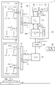
도 2는, 제1의 실시형태에 따른 측정 시스템의 구동 장치의 구성 예를 나타내는 모식도이고,
도 3은, 제1의 실시형태에 따른 측정 시스템의 광 분기 장치의 구성 예를 나타내는 모식도이고,
도 4는, 제1의 실시형태에 따른 측정 시스템의 광전 변환 장치의 구성 예를 나타내는 모식도이고,
도 5는, 제1의 실시형태에 따른 측정 시스템의 구성의 일부를 나타내는 모식도이고,
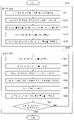
도 6은, 제1의 실시형태에 따른 측정 시스템을 이용한 측정 방법을 설명하기위한 흐름도이고,
도 7a는, 제1의 실시형태에 따른 측정 시스템에 의한 측정 시간의 예를 나타내는 그래프이고,
도 7b는, 제1의 실시형태에 따른 측정 시스템에 의한 측정 시간의 예를 나타내는 표이고,
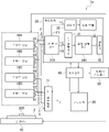
도 8은, 제2의 실시형태에 따른 측정 시스템의 구성을 나타내는 모식도이고,
도 9는, 비교 예의 측정 시스템의 구성을 나타내는 모식도이고,
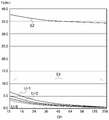
도 10은, 실시형태에 따른 측정 시스템과 비교 예의 측정 시스템의 측정 시간의 비교를 나타내는 그래프이고,
도 11은, 실시형태에 따른 측정 시스템의 유닛 수와 측정 시간의 관계를 나타내는 그래프이다.
2; 반도체 기판
10; 프로브 유닛
11; 광 프로브
12; 전기 프로브
20; 구동 장치
21; 드라이버
30; 처리 장치
31; 광 커플러(optical coupler)
32; 합류기
33; 분광 모듈
34; OE 변환기
40; 제어 장치
50; 프로버 컨트롤러(prober controller)
55; 스테이지
61; 제1 접속반
62; 제2 접속반
71; 제1 절환 회로
72; 제2 절환 회로
110; 광 프로브 어레이
120; 전기 프로브 어레이
200; 광 반도체 소자
300; 적분구(積分球)
301; 차광판
302; 파이버 콜리메이터(fiber collimator)
310; 광 분기 장치
340; 광전 변환 장치
Claims (8)
- 광 반도체 소자의 특성을 측정하는 측정 시스템으로서,
복수의 상기 광 반도체 소자를 구동하는 구동 장치와,
복수의 상기 광 반도체 소자에서의 출사광을 각각 수광(受光)하는 복수의 광 접속 장치를 갖는 프로브 유닛과,
복수의 광전 변환기를 갖는 처리 장치를, 구비하며,
상기 광 접속 장치와 상기 광전 변환기는 1대 1로 접속하여, 상기 광 접속 장치가 수광한 상기 출사광의 적어도 일부가 상기 광전 변환기에 입력하고,
상기 광전 변환기는 입력한 상기 출사광을 전기 신호로 변환하는 것을 특징으로 하는 측정 시스템.
- 제1항에 있어서,
상기 프로브 유닛이 복수의 전기 프로브를 가지며,
상기 구동 장치가, 상기 전기 프로브와 1대 1로 대응하는 복수의 드라이버(driver)를 가지며,
상기 드라이버가, 상기 전기 프로브를 통해서 상기 광 반도체 소자에 구동 전류를 공급하는 것을 특징으로 하는 측정 시스템.
- 제1항 또는 제2항에 있어서,
상기 처리 장치가,
복수의 상기 광 접속 장치가 각각 수광한 상기 출사광의 각각을 제1 분기광(分岐光)과 제2 분기광으로 분기하는 광 분기 장치와,
상기 제1 분기광을 분광(分光)하는 분광 모듈을 더 구비하고,
상기 분광 모듈이, 복수의 상기 광 접속 장치가 수광한 상기 출사광의 상기 제1 분기광을 하나씩 순서대로 분광하는 것을 특징으로 하는 측정 시스템.
- 제3항에 있어서,
상기 광 분기 장치가, 복수의 상기 광 접속 장치와 1대 1로 대응하는 복수의 광 커플러를 가지며,
상기 광 커플러가, 상기 출사광을 상기 제1 분기광과 상기 제2 분기광으로 분기하는 것을 특징으로 하는 측정 시스템.
- 제3항에 있어서,
상기 제2 분기광이 상기 광전 변환기에 입력하는 것을 특징으로 하는 측정 시스템.
- 제1항 또는 제2항에 있어서,
상기 광 접속 장치가, 선단에 상기 출사광이 입사하는 광 프로브인 것을 특징으로 하는 측정 시스템.
- 제1항 또는 제2항에 있어서,
상기 광 접속 장치가, 내부에 상기 출사광이 입사하는 적분구(積分球)인 것을 특징으로 하는 측정 시스템.
- 제1항 또는 제2항에 있어서,
복수의 상기 프로브 유닛을 구비하고,
복수의 상기 프로브 유닛 중 어느 하나와 상기 구동 장치 및 상기 광전 변환기와의 접속을 절환(switch)해서, 상기 프로브 유닛마다 상기 출사광을 처리하는 것을 특징으로 하는 측정 시스템.
Applications Claiming Priority (2)
| Application Number | Priority Date | Filing Date | Title |
|---|---|---|---|
| JP2020210963A JP7525389B2 (ja) | 2020-12-21 | 2020-12-21 | 測定システム |
| JPJP-P-2020-210963 | 2020-12-21 |
Publications (1)
| Publication Number | Publication Date |
|---|---|
| KR20220089618A true KR20220089618A (ko) | 2022-06-28 |
Family
ID=82022211
Family Applications (1)
| Application Number | Title | Priority Date | Filing Date |
|---|---|---|---|
| KR1020210149645A Ceased KR20220089618A (ko) | 2020-12-21 | 2021-11-03 | 측정 시스템 |
Country Status (5)
| Country | Link |
|---|---|
| US (1) | US12379398B2 (ko) |
| JP (1) | JP7525389B2 (ko) |
| KR (1) | KR20220089618A (ko) |
| CN (1) | CN114720832A (ko) |
| TW (1) | TWI785793B (ko) |
Citations (2)
| Publication number | Priority date | Publication date | Assignee | Title |
|---|---|---|---|---|
| JPS6064443A (ja) | 1983-09-20 | 1985-04-13 | Seiko Epson Corp | プロ−ブカ−ド |
| JPS6231136A (ja) | 1985-08-02 | 1987-02-10 | Matsushita Electric Ind Co Ltd | 光半導体素子の評価装置 |
Family Cites Families (15)
| Publication number | Priority date | Publication date | Assignee | Title |
|---|---|---|---|---|
| US4808815A (en) * | 1987-03-23 | 1989-02-28 | Genrad, Inc. | Apparatus for testing light-emitting devices using probe means having a preselected pattern arrangement |
| JPH03133183A (ja) * | 1989-10-18 | 1991-06-06 | Fujitsu Ltd | 発光ダイオードアレイの試験装置 |
| JP3011504B2 (ja) * | 1991-10-25 | 2000-02-21 | 株式会社東芝 | 半導体発光素子の評価装置 |
| JPH05183192A (ja) * | 1991-12-27 | 1993-07-23 | Oki Electric Ind Co Ltd | 面発光・受光素子の検査装置 |
| US20070291198A1 (en) * | 2006-06-16 | 2007-12-20 | Vastview Technology Inc. | Method and device for driving LED-based backlight module |
| CN201141906Y (zh) * | 2007-08-22 | 2008-10-29 | 英业达股份有限公司 | 发光二极管测试装置 |
| CN101770967A (zh) | 2009-01-03 | 2010-07-07 | 上海芯豪微电子有限公司 | 一种共用基底集成电路测试方法、装置和系统 |
| US8476918B2 (en) * | 2010-04-28 | 2013-07-02 | Tsmc Solid State Lighting Ltd. | Apparatus and method for wafer level classification of light emitting device |
| KR101136968B1 (ko) * | 2010-05-25 | 2012-04-19 | 한국생산기술연구원 | 프루브 어레이를 이용한 전기광학 검사장치 |
| US8823406B2 (en) * | 2010-10-20 | 2014-09-02 | Cascade Micotech, Inc. | Systems and methods for simultaneous optical testing of a plurality of devices under test |
| US9040896B2 (en) * | 2011-07-01 | 2015-05-26 | James Albert Walker | Optoelectronic-device wafer probe and method therefor |
| TWI468650B (zh) * | 2012-09-14 | 2015-01-11 | Ind Tech Res Inst | 光學檢測系統及其光學檢測裝置 |
| JP2015226008A (ja) * | 2014-05-29 | 2015-12-14 | 株式会社日本マイクロニクス | 発光素子の検査装置 |
| JP7346259B2 (ja) * | 2019-11-18 | 2023-09-19 | 株式会社日本マイクロニクス | 測定システム |
| JP7492881B2 (ja) * | 2020-08-03 | 2024-05-30 | 株式会社日本マイクロニクス | 測定システムおよび測定方法 |
-
2020
- 2020-12-21 JP JP2020210963A patent/JP7525389B2/ja active Active
-
2021
- 2021-09-11 TW TW110133885A patent/TWI785793B/zh active
- 2021-09-23 US US17/483,150 patent/US12379398B2/en active Active
- 2021-11-03 KR KR1020210149645A patent/KR20220089618A/ko not_active Ceased
- 2021-12-21 CN CN202111569930.5A patent/CN114720832A/zh active Pending
Patent Citations (2)
| Publication number | Priority date | Publication date | Assignee | Title |
|---|---|---|---|---|
| JPS6064443A (ja) | 1983-09-20 | 1985-04-13 | Seiko Epson Corp | プロ−ブカ−ド |
| JPS6231136A (ja) | 1985-08-02 | 1987-02-10 | Matsushita Electric Ind Co Ltd | 光半導体素子の評価装置 |
Also Published As
| Publication number | Publication date |
|---|---|
| JP7525389B2 (ja) | 2024-07-30 |
| US20220196570A1 (en) | 2022-06-23 |
| US12379398B2 (en) | 2025-08-05 |
| JP2022097804A (ja) | 2022-07-01 |
| CN114720832A (zh) | 2022-07-08 |
| TWI785793B (zh) | 2022-12-01 |
| TW202225693A (zh) | 2022-07-01 |
Similar Documents
| Publication | Publication Date | Title |
|---|---|---|
| US11680870B2 (en) | Opto electrical test measurement system for integrated photonic devices and circuits | |
| US20130001405A1 (en) | Optoelectronic-Device Wafer Probe and Method Therefor | |
| CN206920661U (zh) | 高速光收发模块 | |
| JP2020530121A (ja) | 光電子チップを接触させるための位置公差に無感応な接触モジュール | |
| CN102075242A (zh) | 无源器件损耗分析装置 | |
| WO2016081720A1 (en) | Planar lightwave circuit active connector | |
| US11784720B2 (en) | Optical module | |
| CN111982166B (zh) | 针对多芯光纤分光耦合的光电探测器阵列及系统 | |
| US5066097A (en) | Connector for an optical cable | |
| Dumke et al. | Power transmission by optical fibers for component inherent communication | |
| CN112985487B (zh) | 阵列式光电探测器测试系统 | |
| TWI776279B (zh) | 測量系統 | |
| KR20090053490A (ko) | 광학 전송수단을 구비한 프루브 카드 및 메모리 테스터 | |
| KR20220089618A (ko) | 측정 시스템 | |
| JPS6231136A (ja) | 光半導体素子の評価装置 | |
| Herick et al. | Realization of an opto-electronic bias for pulse-driven Josephson voltage standards at PTB | |
| US12174238B2 (en) | Intelligent wafer-level testing of photonic devices | |
| KR19990078216A (ko) | 광분기모듈 | |
| US7015458B2 (en) | High density fiber optic output interface and system | |
| Matveev et al. | Organizing energy-and-information exchange between devices for controlling the shape of a transformable antenna, using fiber-optic technology | |
| US12197051B2 (en) | Optical inspection circuit and optical inspection method | |
| JP2010016110A (ja) | アレイ型発光素子の検査装置及び検査方法 | |
| US20130322829A1 (en) | Optical-electrical transmission assembly and optical transmission module using the same | |
| KR100289147B1 (ko) | 광신호 송수신모듈의 성능 시험장치 | |
| CN117289641B (zh) | 光芯片的晶圆测试系统 |
Legal Events
| Date | Code | Title | Description |
|---|---|---|---|
| PA0109 | Patent application |
Patent event code: PA01091R01D Comment text: Patent Application Patent event date: 20211103 |
|
| PA0201 | Request for examination | ||
| PG1501 | Laying open of application | ||
| E902 | Notification of reason for refusal | ||
| PE0902 | Notice of grounds for rejection |
Comment text: Notification of reason for refusal Patent event date: 20231025 Patent event code: PE09021S01D |
|
| E601 | Decision to refuse application | ||
| PE0601 | Decision on rejection of patent |
Patent event date: 20240430 Comment text: Decision to Refuse Application Patent event code: PE06012S01D Patent event date: 20231025 Comment text: Notification of reason for refusal Patent event code: PE06011S01I |
|
| J201 | Request for trial against refusal decision | ||
| PJ0201 | Trial against decision of rejection |
Patent event date: 20240731 Comment text: Request for Trial against Decision on Refusal Patent event code: PJ02012R01D Appeal kind category: Appeal against decision to decline refusal Appeal identifier: 2024101001698 Request date: 20240731 |
|
| J301 | Trial decision |
Free format text: TRIAL NUMBER: 2024101001698; TRIAL DECISION FOR APPEAL AGAINST DECISION TO DECLINE REFUSAL REQUESTED 20240731 Effective date: 20250612 |
|
| PJ1301 | Trial decision |
Patent event code: PJ13011S01D Patent event date: 20250612 Comment text: Trial Decision on Objection to Decision on Refusal Appeal kind category: Appeal against decision to decline refusal Request date: 20240731 Decision date: 20250612 Appeal identifier: 2024101001698 |