KR20220143579A - 유동성 탄소 층으로 갭을 충진하는 방법 - Google Patents
유동성 탄소 층으로 갭을 충진하는 방법 Download PDFInfo
- Publication number
- KR20220143579A KR20220143579A KR1020220044269A KR20220044269A KR20220143579A KR 20220143579 A KR20220143579 A KR 20220143579A KR 1020220044269 A KR1020220044269 A KR 1020220044269A KR 20220044269 A KR20220044269 A KR 20220044269A KR 20220143579 A KR20220143579 A KR 20220143579A
- Authority
- KR
- South Korea
- Prior art keywords
- carbon layer
- carbon
- forming
- reaction chamber
- flux
- Prior art date
- Legal status (The legal status is an assumption and is not a legal conclusion. Google has not performed a legal analysis and makes no representation as to the accuracy of the status listed.)
- Pending
Links
Images


Classifications
-
- H—ELECTRICITY
- H10—SEMICONDUCTOR DEVICES; ELECTRIC SOLID-STATE DEVICES NOT OTHERWISE PROVIDED FOR
- H10P—GENERIC PROCESSES OR APPARATUS FOR THE MANUFACTURE OR TREATMENT OF DEVICES COVERED BY CLASS H10
- H10P14/00—Formation of materials, e.g. in the shape of layers or pillars
- H10P14/60—Formation of materials, e.g. in the shape of layers or pillars of insulating materials
- H10P14/63—Formation of materials, e.g. in the shape of layers or pillars of insulating materials characterised by the formation processes
- H10P14/6326—Deposition processes
- H10P14/6328—Deposition from the gas or vapour phase
- H10P14/6334—Deposition from the gas or vapour phase using decomposition or reaction of gaseous or vapour phase compounds, i.e. chemical vapour deposition
- H10P14/6339—Deposition from the gas or vapour phase using decomposition or reaction of gaseous or vapour phase compounds, i.e. chemical vapour deposition deposition by cyclic CVD, e.g. ALD, ALE or pulsed CVD
-
- C—CHEMISTRY; METALLURGY
- C23—COATING METALLIC MATERIAL; COATING MATERIAL WITH METALLIC MATERIAL; CHEMICAL SURFACE TREATMENT; DIFFUSION TREATMENT OF METALLIC MATERIAL; COATING BY VACUUM EVAPORATION, BY SPUTTERING, BY ION IMPLANTATION OR BY CHEMICAL VAPOUR DEPOSITION, IN GENERAL; INHIBITING CORROSION OF METALLIC MATERIAL OR INCRUSTATION IN GENERAL
- C23C—COATING METALLIC MATERIAL; COATING MATERIAL WITH METALLIC MATERIAL; SURFACE TREATMENT OF METALLIC MATERIAL BY DIFFUSION INTO THE SURFACE, BY CHEMICAL CONVERSION OR SUBSTITUTION; COATING BY VACUUM EVAPORATION, BY SPUTTERING, BY ION IMPLANTATION OR BY CHEMICAL VAPOUR DEPOSITION, IN GENERAL
- C23C26/00—Coating not provided for in groups C23C2/00 - C23C24/00
-
- H—ELECTRICITY
- H01—ELECTRIC ELEMENTS
- H01J—ELECTRIC DISCHARGE TUBES OR DISCHARGE LAMPS
- H01J37/00—Discharge tubes with provision for introducing objects or material to be exposed to the discharge, e.g. for the purpose of examination or processing thereof
- H01J37/32—Gas-filled discharge tubes
- H01J37/32431—Constructional details of the reactor
- H01J37/3244—Gas supply means
- H01J37/32449—Gas control, e.g. control of the gas flow
-
- H01L21/0234—
-
- B—PERFORMING OPERATIONS; TRANSPORTING
- B05—SPRAYING OR ATOMISING IN GENERAL; APPLYING FLUENT MATERIALS TO SURFACES, IN GENERAL
- B05D—PROCESSES FOR APPLYING FLUENT MATERIALS TO SURFACES, IN GENERAL
- B05D1/00—Processes for applying liquids or other fluent materials
- B05D1/62—Plasma-deposition of organic layers
-
- C—CHEMISTRY; METALLURGY
- C23—COATING METALLIC MATERIAL; COATING MATERIAL WITH METALLIC MATERIAL; CHEMICAL SURFACE TREATMENT; DIFFUSION TREATMENT OF METALLIC MATERIAL; COATING BY VACUUM EVAPORATION, BY SPUTTERING, BY ION IMPLANTATION OR BY CHEMICAL VAPOUR DEPOSITION, IN GENERAL; INHIBITING CORROSION OF METALLIC MATERIAL OR INCRUSTATION IN GENERAL
- C23C—COATING METALLIC MATERIAL; COATING MATERIAL WITH METALLIC MATERIAL; SURFACE TREATMENT OF METALLIC MATERIAL BY DIFFUSION INTO THE SURFACE, BY CHEMICAL CONVERSION OR SUBSTITUTION; COATING BY VACUUM EVAPORATION, BY SPUTTERING, BY ION IMPLANTATION OR BY CHEMICAL VAPOUR DEPOSITION, IN GENERAL
- C23C16/00—Chemical coating by decomposition of gaseous compounds, without leaving reaction products of surface material in the coating, i.e. chemical vapour deposition [CVD] processes
- C23C16/04—Coating on selected surface areas, e.g. using masks
- C23C16/045—Coating cavities or hollow spaces, e.g. interior of tubes; Infiltration of porous substrates
-
- C—CHEMISTRY; METALLURGY
- C23—COATING METALLIC MATERIAL; COATING MATERIAL WITH METALLIC MATERIAL; CHEMICAL SURFACE TREATMENT; DIFFUSION TREATMENT OF METALLIC MATERIAL; COATING BY VACUUM EVAPORATION, BY SPUTTERING, BY ION IMPLANTATION OR BY CHEMICAL VAPOUR DEPOSITION, IN GENERAL; INHIBITING CORROSION OF METALLIC MATERIAL OR INCRUSTATION IN GENERAL
- C23C—COATING METALLIC MATERIAL; COATING MATERIAL WITH METALLIC MATERIAL; SURFACE TREATMENT OF METALLIC MATERIAL BY DIFFUSION INTO THE SURFACE, BY CHEMICAL CONVERSION OR SUBSTITUTION; COATING BY VACUUM EVAPORATION, BY SPUTTERING, BY ION IMPLANTATION OR BY CHEMICAL VAPOUR DEPOSITION, IN GENERAL
- C23C16/00—Chemical coating by decomposition of gaseous compounds, without leaving reaction products of surface material in the coating, i.e. chemical vapour deposition [CVD] processes
- C23C16/22—Chemical coating by decomposition of gaseous compounds, without leaving reaction products of surface material in the coating, i.e. chemical vapour deposition [CVD] processes characterised by the deposition of inorganic material, other than metallic material
- C23C16/26—Deposition of carbon only
-
- C—CHEMISTRY; METALLURGY
- C23—COATING METALLIC MATERIAL; COATING MATERIAL WITH METALLIC MATERIAL; CHEMICAL SURFACE TREATMENT; DIFFUSION TREATMENT OF METALLIC MATERIAL; COATING BY VACUUM EVAPORATION, BY SPUTTERING, BY ION IMPLANTATION OR BY CHEMICAL VAPOUR DEPOSITION, IN GENERAL; INHIBITING CORROSION OF METALLIC MATERIAL OR INCRUSTATION IN GENERAL
- C23C—COATING METALLIC MATERIAL; COATING MATERIAL WITH METALLIC MATERIAL; SURFACE TREATMENT OF METALLIC MATERIAL BY DIFFUSION INTO THE SURFACE, BY CHEMICAL CONVERSION OR SUBSTITUTION; COATING BY VACUUM EVAPORATION, BY SPUTTERING, BY ION IMPLANTATION OR BY CHEMICAL VAPOUR DEPOSITION, IN GENERAL
- C23C16/00—Chemical coating by decomposition of gaseous compounds, without leaving reaction products of surface material in the coating, i.e. chemical vapour deposition [CVD] processes
- C23C16/44—Chemical coating by decomposition of gaseous compounds, without leaving reaction products of surface material in the coating, i.e. chemical vapour deposition [CVD] processes characterised by the method of coating
- C23C16/4401—Means for minimising impurities, e.g. dust, moisture or residual gas, in the reaction chamber
- C23C16/4409—Means for minimising impurities, e.g. dust, moisture or residual gas, in the reaction chamber characterised by sealing means
-
- C—CHEMISTRY; METALLURGY
- C23—COATING METALLIC MATERIAL; COATING MATERIAL WITH METALLIC MATERIAL; CHEMICAL SURFACE TREATMENT; DIFFUSION TREATMENT OF METALLIC MATERIAL; COATING BY VACUUM EVAPORATION, BY SPUTTERING, BY ION IMPLANTATION OR BY CHEMICAL VAPOUR DEPOSITION, IN GENERAL; INHIBITING CORROSION OF METALLIC MATERIAL OR INCRUSTATION IN GENERAL
- C23C—COATING METALLIC MATERIAL; COATING MATERIAL WITH METALLIC MATERIAL; SURFACE TREATMENT OF METALLIC MATERIAL BY DIFFUSION INTO THE SURFACE, BY CHEMICAL CONVERSION OR SUBSTITUTION; COATING BY VACUUM EVAPORATION, BY SPUTTERING, BY ION IMPLANTATION OR BY CHEMICAL VAPOUR DEPOSITION, IN GENERAL
- C23C16/00—Chemical coating by decomposition of gaseous compounds, without leaving reaction products of surface material in the coating, i.e. chemical vapour deposition [CVD] processes
- C23C16/44—Chemical coating by decomposition of gaseous compounds, without leaving reaction products of surface material in the coating, i.e. chemical vapour deposition [CVD] processes characterised by the method of coating
- C23C16/455—Chemical coating by decomposition of gaseous compounds, without leaving reaction products of surface material in the coating, i.e. chemical vapour deposition [CVD] processes characterised by the method of coating characterised by the method used for introducing gases into reaction chamber or for modifying gas flows in reaction chamber
- C23C16/45523—Pulsed gas flow or change of composition over time
- C23C16/45525—Atomic layer deposition [ALD]
- C23C16/45527—Atomic layer deposition [ALD] characterized by the ALD cycle, e.g. different flows or temperatures during half-reactions, unusual pulsing sequence, use of precursor mixtures or auxiliary reactants or activations
- C23C16/45536—Use of plasma, radiation or electromagnetic fields
- C23C16/4554—Plasma being used non-continuously in between ALD reactions
-
- C—CHEMISTRY; METALLURGY
- C23—COATING METALLIC MATERIAL; COATING MATERIAL WITH METALLIC MATERIAL; CHEMICAL SURFACE TREATMENT; DIFFUSION TREATMENT OF METALLIC MATERIAL; COATING BY VACUUM EVAPORATION, BY SPUTTERING, BY ION IMPLANTATION OR BY CHEMICAL VAPOUR DEPOSITION, IN GENERAL; INHIBITING CORROSION OF METALLIC MATERIAL OR INCRUSTATION IN GENERAL
- C23C—COATING METALLIC MATERIAL; COATING MATERIAL WITH METALLIC MATERIAL; SURFACE TREATMENT OF METALLIC MATERIAL BY DIFFUSION INTO THE SURFACE, BY CHEMICAL CONVERSION OR SUBSTITUTION; COATING BY VACUUM EVAPORATION, BY SPUTTERING, BY ION IMPLANTATION OR BY CHEMICAL VAPOUR DEPOSITION, IN GENERAL
- C23C16/00—Chemical coating by decomposition of gaseous compounds, without leaving reaction products of surface material in the coating, i.e. chemical vapour deposition [CVD] processes
- C23C16/44—Chemical coating by decomposition of gaseous compounds, without leaving reaction products of surface material in the coating, i.e. chemical vapour deposition [CVD] processes characterised by the method of coating
- C23C16/455—Chemical coating by decomposition of gaseous compounds, without leaving reaction products of surface material in the coating, i.e. chemical vapour deposition [CVD] processes characterised by the method of coating characterised by the method used for introducing gases into reaction chamber or for modifying gas flows in reaction chamber
- C23C16/45523—Pulsed gas flow or change of composition over time
- C23C16/45525—Atomic layer deposition [ALD]
- C23C16/45527—Atomic layer deposition [ALD] characterized by the ALD cycle, e.g. different flows or temperatures during half-reactions, unusual pulsing sequence, use of precursor mixtures or auxiliary reactants or activations
- C23C16/45536—Use of plasma, radiation or electromagnetic fields
- C23C16/45542—Plasma being used non-continuously during the ALD reactions
-
- C—CHEMISTRY; METALLURGY
- C23—COATING METALLIC MATERIAL; COATING MATERIAL WITH METALLIC MATERIAL; CHEMICAL SURFACE TREATMENT; DIFFUSION TREATMENT OF METALLIC MATERIAL; COATING BY VACUUM EVAPORATION, BY SPUTTERING, BY ION IMPLANTATION OR BY CHEMICAL VAPOUR DEPOSITION, IN GENERAL; INHIBITING CORROSION OF METALLIC MATERIAL OR INCRUSTATION IN GENERAL
- C23C—COATING METALLIC MATERIAL; COATING MATERIAL WITH METALLIC MATERIAL; SURFACE TREATMENT OF METALLIC MATERIAL BY DIFFUSION INTO THE SURFACE, BY CHEMICAL CONVERSION OR SUBSTITUTION; COATING BY VACUUM EVAPORATION, BY SPUTTERING, BY ION IMPLANTATION OR BY CHEMICAL VAPOUR DEPOSITION, IN GENERAL
- C23C16/00—Chemical coating by decomposition of gaseous compounds, without leaving reaction products of surface material in the coating, i.e. chemical vapour deposition [CVD] processes
- C23C16/44—Chemical coating by decomposition of gaseous compounds, without leaving reaction products of surface material in the coating, i.e. chemical vapour deposition [CVD] processes characterised by the method of coating
- C23C16/455—Chemical coating by decomposition of gaseous compounds, without leaving reaction products of surface material in the coating, i.e. chemical vapour deposition [CVD] processes characterised by the method of coating characterised by the method used for introducing gases into reaction chamber or for modifying gas flows in reaction chamber
- C23C16/45523—Pulsed gas flow or change of composition over time
- C23C16/45525—Atomic layer deposition [ALD]
- C23C16/45544—Atomic layer deposition [ALD] characterized by the apparatus
-
- C—CHEMISTRY; METALLURGY
- C23—COATING METALLIC MATERIAL; COATING MATERIAL WITH METALLIC MATERIAL; CHEMICAL SURFACE TREATMENT; DIFFUSION TREATMENT OF METALLIC MATERIAL; COATING BY VACUUM EVAPORATION, BY SPUTTERING, BY ION IMPLANTATION OR BY CHEMICAL VAPOUR DEPOSITION, IN GENERAL; INHIBITING CORROSION OF METALLIC MATERIAL OR INCRUSTATION IN GENERAL
- C23C—COATING METALLIC MATERIAL; COATING MATERIAL WITH METALLIC MATERIAL; SURFACE TREATMENT OF METALLIC MATERIAL BY DIFFUSION INTO THE SURFACE, BY CHEMICAL CONVERSION OR SUBSTITUTION; COATING BY VACUUM EVAPORATION, BY SPUTTERING, BY ION IMPLANTATION OR BY CHEMICAL VAPOUR DEPOSITION, IN GENERAL
- C23C16/00—Chemical coating by decomposition of gaseous compounds, without leaving reaction products of surface material in the coating, i.e. chemical vapour deposition [CVD] processes
- C23C16/44—Chemical coating by decomposition of gaseous compounds, without leaving reaction products of surface material in the coating, i.e. chemical vapour deposition [CVD] processes characterised by the method of coating
- C23C16/455—Chemical coating by decomposition of gaseous compounds, without leaving reaction products of surface material in the coating, i.e. chemical vapour deposition [CVD] processes characterised by the method of coating characterised by the method used for introducing gases into reaction chamber or for modifying gas flows in reaction chamber
- C23C16/45523—Pulsed gas flow or change of composition over time
- C23C16/45525—Atomic layer deposition [ALD]
- C23C16/45553—Atomic layer deposition [ALD] characterized by the use of precursors specially adapted for ALD
-
- C—CHEMISTRY; METALLURGY
- C23—COATING METALLIC MATERIAL; COATING MATERIAL WITH METALLIC MATERIAL; CHEMICAL SURFACE TREATMENT; DIFFUSION TREATMENT OF METALLIC MATERIAL; COATING BY VACUUM EVAPORATION, BY SPUTTERING, BY ION IMPLANTATION OR BY CHEMICAL VAPOUR DEPOSITION, IN GENERAL; INHIBITING CORROSION OF METALLIC MATERIAL OR INCRUSTATION IN GENERAL
- C23C—COATING METALLIC MATERIAL; COATING MATERIAL WITH METALLIC MATERIAL; SURFACE TREATMENT OF METALLIC MATERIAL BY DIFFUSION INTO THE SURFACE, BY CHEMICAL CONVERSION OR SUBSTITUTION; COATING BY VACUUM EVAPORATION, BY SPUTTERING, BY ION IMPLANTATION OR BY CHEMICAL VAPOUR DEPOSITION, IN GENERAL
- C23C16/00—Chemical coating by decomposition of gaseous compounds, without leaving reaction products of surface material in the coating, i.e. chemical vapour deposition [CVD] processes
- C23C16/44—Chemical coating by decomposition of gaseous compounds, without leaving reaction products of surface material in the coating, i.e. chemical vapour deposition [CVD] processes characterised by the method of coating
- C23C16/52—Controlling or regulating the coating process
-
- C—CHEMISTRY; METALLURGY
- C23—COATING METALLIC MATERIAL; COATING MATERIAL WITH METALLIC MATERIAL; CHEMICAL SURFACE TREATMENT; DIFFUSION TREATMENT OF METALLIC MATERIAL; COATING BY VACUUM EVAPORATION, BY SPUTTERING, BY ION IMPLANTATION OR BY CHEMICAL VAPOUR DEPOSITION, IN GENERAL; INHIBITING CORROSION OF METALLIC MATERIAL OR INCRUSTATION IN GENERAL
- C23C—COATING METALLIC MATERIAL; COATING MATERIAL WITH METALLIC MATERIAL; SURFACE TREATMENT OF METALLIC MATERIAL BY DIFFUSION INTO THE SURFACE, BY CHEMICAL CONVERSION OR SUBSTITUTION; COATING BY VACUUM EVAPORATION, BY SPUTTERING, BY ION IMPLANTATION OR BY CHEMICAL VAPOUR DEPOSITION, IN GENERAL
- C23C16/00—Chemical coating by decomposition of gaseous compounds, without leaving reaction products of surface material in the coating, i.e. chemical vapour deposition [CVD] processes
- C23C16/56—After-treatment
-
- H01L21/02115—
-
- H01L21/02205—
-
- H01L21/02274—
-
- H01L21/0228—
-
- H01L21/31051—
-
- H—ELECTRICITY
- H10—SEMICONDUCTOR DEVICES; ELECTRIC SOLID-STATE DEVICES NOT OTHERWISE PROVIDED FOR
- H10P—GENERIC PROCESSES OR APPARATUS FOR THE MANUFACTURE OR TREATMENT OF DEVICES COVERED BY CLASS H10
- H10P14/00—Formation of materials, e.g. in the shape of layers or pillars
- H10P14/60—Formation of materials, e.g. in the shape of layers or pillars of insulating materials
- H10P14/63—Formation of materials, e.g. in the shape of layers or pillars of insulating materials characterised by the formation processes
- H10P14/6326—Deposition processes
- H10P14/6328—Deposition from the gas or vapour phase
- H10P14/6334—Deposition from the gas or vapour phase using decomposition or reaction of gaseous or vapour phase compounds, i.e. chemical vapour deposition
- H10P14/6336—Deposition from the gas or vapour phase using decomposition or reaction of gaseous or vapour phase compounds, i.e. chemical vapour deposition in the presence of a plasma [PECVD]
-
- H—ELECTRICITY
- H10—SEMICONDUCTOR DEVICES; ELECTRIC SOLID-STATE DEVICES NOT OTHERWISE PROVIDED FOR
- H10P—GENERIC PROCESSES OR APPARATUS FOR THE MANUFACTURE OR TREATMENT OF DEVICES COVERED BY CLASS H10
- H10P14/00—Formation of materials, e.g. in the shape of layers or pillars
- H10P14/60—Formation of materials, e.g. in the shape of layers or pillars of insulating materials
- H10P14/65—Formation of materials, e.g. in the shape of layers or pillars of insulating materials characterised by treatments performed before or after the formation of the materials
- H10P14/6516—Formation of materials, e.g. in the shape of layers or pillars of insulating materials characterised by treatments performed before or after the formation of the materials of treatments performed after formation of the materials
- H10P14/6529—Formation of materials, e.g. in the shape of layers or pillars of insulating materials characterised by treatments performed before or after the formation of the materials of treatments performed after formation of the materials by exposure to a gas or vapour
- H10P14/6532—Formation of materials, e.g. in the shape of layers or pillars of insulating materials characterised by treatments performed before or after the formation of the materials of treatments performed after formation of the materials by exposure to a gas or vapour by exposure to a plasma
-
- H—ELECTRICITY
- H10—SEMICONDUCTOR DEVICES; ELECTRIC SOLID-STATE DEVICES NOT OTHERWISE PROVIDED FOR
- H10P—GENERIC PROCESSES OR APPARATUS FOR THE MANUFACTURE OR TREATMENT OF DEVICES COVERED BY CLASS H10
- H10P14/00—Formation of materials, e.g. in the shape of layers or pillars
- H10P14/60—Formation of materials, e.g. in the shape of layers or pillars of insulating materials
- H10P14/66—Formation of materials, e.g. in the shape of layers or pillars of insulating materials characterised by the type of materials
- H10P14/668—Formation of materials, e.g. in the shape of layers or pillars of insulating materials characterised by the type of materials the materials being characterised by the deposition precursor materials
-
- H—ELECTRICITY
- H10—SEMICONDUCTOR DEVICES; ELECTRIC SOLID-STATE DEVICES NOT OTHERWISE PROVIDED FOR
- H10P—GENERIC PROCESSES OR APPARATUS FOR THE MANUFACTURE OR TREATMENT OF DEVICES COVERED BY CLASS H10
- H10P14/00—Formation of materials, e.g. in the shape of layers or pillars
- H10P14/60—Formation of materials, e.g. in the shape of layers or pillars of insulating materials
- H10P14/68—Organic materials, e.g. photoresists
- H10P14/683—Organic materials, e.g. photoresists carbon-based polymeric organic materials, e.g. polyimides, poly cyclobutene or PVC
-
- H—ELECTRICITY
- H10—SEMICONDUCTOR DEVICES; ELECTRIC SOLID-STATE DEVICES NOT OTHERWISE PROVIDED FOR
- H10P—GENERIC PROCESSES OR APPARATUS FOR THE MANUFACTURE OR TREATMENT OF DEVICES COVERED BY CLASS H10
- H10P14/00—Formation of materials, e.g. in the shape of layers or pillars
- H10P14/60—Formation of materials, e.g. in the shape of layers or pillars of insulating materials
- H10P14/69—Inorganic materials
- H10P14/6902—Inorganic materials composed of carbon, e.g. alpha-C, diamond or hydrogen doped carbon
-
- H—ELECTRICITY
- H10—SEMICONDUCTOR DEVICES; ELECTRIC SOLID-STATE DEVICES NOT OTHERWISE PROVIDED FOR
- H10P—GENERIC PROCESSES OR APPARATUS FOR THE MANUFACTURE OR TREATMENT OF DEVICES COVERED BY CLASS H10
- H10P95/00—Generic processes or apparatus for manufacture or treatments not covered by the other groups of this subclass
- H10P95/06—Planarisation of inorganic insulating materials
-
- H—ELECTRICITY
- H01—ELECTRIC ELEMENTS
- H01J—ELECTRIC DISCHARGE TUBES OR DISCHARGE LAMPS
- H01J2237/00—Discharge tubes exposing object to beam, e.g. for analysis treatment, etching, imaging
- H01J2237/32—Processing objects by plasma generation
- H01J2237/33—Processing objects by plasma generation characterised by the type of processing
- H01J2237/332—Coating
Landscapes
- Chemical & Material Sciences (AREA)
- Engineering & Computer Science (AREA)
- Organic Chemistry (AREA)
- Chemical Kinetics & Catalysis (AREA)
- Materials Engineering (AREA)
- Mechanical Engineering (AREA)
- Metallurgy (AREA)
- General Chemical & Material Sciences (AREA)
- Plasma & Fusion (AREA)
- Physics & Mathematics (AREA)
- Inorganic Chemistry (AREA)
- Electromagnetism (AREA)
- Analytical Chemistry (AREA)
- Chemical Vapour Deposition (AREA)
- Thin Film Transistor (AREA)
- Carbon And Carbon Compounds (AREA)
Abstract
Description
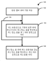
도 1은 본 개시의 예시적 구현예에 따른 방법을 나타낸다.
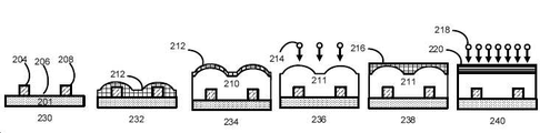
도 2는 본 개시의 적어도 하나의 구현예에 따라 형성된 구조체를 나타낸다.
도 3은 본 개시의 예시적 구현예에 따른 방법을 나타낸다.
도 4는 본 개시의 예시적 구현예에 따른 시간 순서 다이어그램을 나타낸다.
도 5는 본 개시의 예시적인 구현예에 따른 다중 트렌치 구조체를 나타낸다.
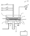
도 6은 본 개시의 예시적 구현예에 따른 시스템을 나타낸다.
도면의 구성 요소들은 간략하고 명료하게 도시되어 있으며, 반드시 축적대로 도시되지 않았음을 이해할 것이다. 예를 들어, 본 개시에서 예시된 구현예의 이해를 돕기 위해 도면 중 일부 구성 요소의 치수는 다른 구성 요소에 비해 과장될 수 있다.

Claims (22)
- 방법으로서,
표면 상에 형성된 하나 이상의 리세스를 포함한 기판을, 반응 챔버에 제공하는 단계;
상기 표면 위에 하나 이상의 제1 탄소 층을 형성하는 단계(상기 하나 이상의 제1 탄소 층 중 적어도 하나는 제1 초기 유동성을 가짐); 및
상기 하나 이상의 제1 탄소 층 위에 제2 탄소 층을 형성하는 단계(상기 제2 탄소 층은 제2 초기 유동성을 가짐)를 포함하되,
상기 제2 초기 유동성은 상기 제1 초기 유동성보다 큰, 방법. - 제1항에 있어서, 상기 하나 이상의 리세스 중 적어도 하나의 리세스는 다중 트렌치 구조체를 포함하는, 방법.
- 제1항 또는 제2항에 있어서, 상기 제2 탄소 층은 상기 하나 이상의 제1 탄소 층 중 적어도 하나보다 두꺼운, 방법.
- 제1항 내지 제3항 중 어느 한 항에 있어서, 상기 하나 이상의 제1 탄소 층을 형성하는 단계는, 상기 하나 이상의 리세스 내에 제1 초기 점성 층을 형성하는 단계 및 제1 플라즈마 공정을 사용하여 상기 제1 초기 점성 층을 처리하는 단계의 하나 이상의 사이클을 포함하는, 방법.
- 제1항 내지 제4항 중 어느 한 항에 있어서, 상기 제2 탄소 층을 형성하는 단계는, 제2 초기 점성 층을 형성하는 단계, 및 제2 플라즈마 공정을 사용하여 상기 제2 초기 점성 층을 처리하는 단계를 포함하는, 방법.
- 제5항에 있어서, 상기 제1 플라즈마 공정은 제1 플라즈마 전력을 포함하고, 상기 제2 플라즈마 공정은 제2 플라즈마 전력을 포함하되, 상기 제2 플라즈마 전력은 상기 제1 플라즈마 전력보다 큰, 방법.
- 제4항 내지 제6항 중 어느 한 항에 있어서, 상기 제1 초기 점성 층은 제1 처리 시간 동안 상기 제1 플라즈마 공정으로 처리되고, 상기 제2 초기 점성 층은 제2 처리 시간 동안 상기 제2 플라즈마 공정으로 처리되며, 상기 제2 처리 시간은 상기 제1 처리 시간보다 긴, 방법.
- 제4항 내지 제6항 중 어느 한 항에 있어서, 상기 제1 플라즈마 공정은 제1 이온 에너지 레벨 및 제1 플럭스를 포함하고, 상기 제2 플라즈마 공정은 제2 이온 에너지 레벨 및 제2 플럭스를 포함하되, 상기 제2 이온 에너지 레벨은 상기 제1 이온 에너지 레벨보다 큰, 방법.
- 제8항에 있어서, 상기 제2 플럭스는 상기 제1 플럭스보다 큰 방법.
- 제4항 내지 제9항 중 어느 한 항에 있어서, 상기 제2 탄소 층을 형성하는 단계 동안의 증착 시간은, 하나 이상의 제1 탄소 층을 형성하는 단계 동안의 증착 시간보다 긴, 방법.
- 제1항 내지 제10항 중 어느 한 항에 있어서, 상기 제2 탄소 층의 표면은 평탄화되는, 방법.
- 제1항 내지 제11항 중 어느 한 항에 있어서, 상기 하나 이상의 제1 탄소 층을 형성하는 단계 동안에, 상기 반응 챔버 내의 온도는 100°C 미만인, 방법.
- 제1항 내지 제12항 중 어느 한 항에 있어서, 상기 제2 탄소 층을 형성하는 단계 동안에, 상기 반응 챔버 내의 온도는 100°C 미만인, 방법.
- 제1항 내지 제13항 중 어느 한 항에 있어서, 상기 제1 플라즈마 공정 또는 상기 제2 플라즈마 공정 중 적어도 하나는 He, Ar, 및 N2 중 하나 이상으로부터 여기된 종을 형성하는 단계를 포함하는, 방법.
- 제1항 내지 제14항 중 어느 한 항에 있어서, 상기 하나 이상의 제1 탄소 층을 형성하는 단계는 제1 횟수만큼 반복되고, 상기 제2 탄소 층을 형성하는 단계는 제2 횟수만큼 반복되며, 상기 제1 횟수는 상기 제2 횟수보다 큰, 방법.
- 제1항 내지 제15항 중 어느 한 항에 있어서, 상기 하나 이상의 제1 탄소 층을 형성하는 단계는, 화학 조성식 CxHyNzOa(x는 2 이상인 자연수이고, y는 자연수이고, z는 0이거나 자연수이고, a는 0이거나 자연수임)로 표시된 탄소 전구체를 상기 반응 챔버에 제공하는 단계를 포함하는, 방법.
- 제1항 내지 제16항 중 어느 한 항에 있어서, 상기 제2 탄소 층을 형성하는 단계는, 화학 조성식 CxHyNzOa(x는 2 이상인 자연수이고, y는 자연수이고, z는 0이거나 자연수이고, a는 0이거나 자연수임)로 표시된 탄소 전구체를 상기 반응 챔버에 제공하는 단계를 포함하는, 방법.
- 제1항 내지 제17항 중 어느 한 항에 있어서, 상기 하나 이상의 제1 탄소 층을 형성하는 단계는, 사이클 당 제1 성장 레벨을 포함하고, 상기 제2 탄소 층을 형성하는 단계는, 사이클 당 제2 성장 레벨을 포함하되, 상기 사이클 당 제2 성장 레벨은 사이클 당 제1 성장 레벨보다 큰, 방법.
- 방법으로서,
표면 상에 형성된 하나 이상의 리세스를 포함한 기판을, 반응 챔버에 제공하는 단계;
제1 초기 유동성을 갖는 제1 초기 유동성 탄소 층을 증착하는 단계와 제1 초기 유동성 탄소 층을 제1 이온 에너지 레벨 및 제1 플럭스로 처리하는 단계에 의해, 상기 표면 위에 제1 탄소 층을 형성하는 단계;
제2 초기 유동성을 갖는 제2 초기 유동성 탄소 층을 증착하는 단계와 제2 초기 유동성 탄소 층을 제2 이온 에너지 레벨 및 제2 플럭스로 처리하는 단계에 의해, 상기 제1 탄소 층 위에 제2 탄소 층을 형성하는 단계를 포함하되,
상기 제2 초기 유동성은 상기 제1 초기 유동성보다 크고,
상기 제2 이온 에너지 레벨은 상기 제1 이온 에너지 레벨보다 큰 것 또는 상기 제2 플럭스는 상기 제1 플럭스보다 더 큰 것 중 적어도 하나인, 방법. - 제1항 내지 제19항 중 어느 한 항의 방법에 따라 형성된 구조체.
- 시스템으로서,
반응 챔버;
탄소 전구체 공급원;
불활성 가스 공급원;
플라즈마 전력 공급원;
배기 공급원; 및
제어기를 포함하되,
상기 제어기는, 상기 반응 챔버 내로 상기 탄소 전구체의 가스 흐름을 제어하여 제1 탄소 층 및 상기 제1 탄소 층 위에 제2 탄소 층을 형성하도록 구성되고,
상기 제1 탄소 층은 제1 두께 및 제1 초기 유동성을 포함하고, 상기 제2 탄소 층은 제2 두께 및 제2 초기 유동성을 포함하되,
상기 제2 두께는 상기 제1 두께보다 큰 것 및 상기 제2 유동성은 상기 제1 유동성보다 큰 것 중 적어도 하나인, 시스템. - 제21항에 있어서, 상기 제어기는, 상기 제1 탄소 층을 제1 이온 에너지 레벨 및 제1 플럭스로 처리하는 제1 플라즈마 공정을 제어하도록 구성되고, 상기 제어기는, 상기 제2 탄소 층을 제2 이온 에너지 레벨 및 제2 플럭스로 처리하는 제2 플라즈마 공정을 제어하도록 구성되며,
상기 제2 이온 에너지 레벨은 상기 제1 이온 에너지 레벨보다 큰 것 및 상기 제2 플럭스는 상기 제1 플럭스보다 더 큰 것 중 적어도 하나인, 시스템.
Applications Claiming Priority (2)
| Application Number | Priority Date | Filing Date | Title |
|---|---|---|---|
| US202163175979P | 2021-04-16 | 2021-04-16 | |
| US63/175,979 | 2021-04-16 |
Publications (1)
| Publication Number | Publication Date |
|---|---|
| KR20220143579A true KR20220143579A (ko) | 2022-10-25 |
Family
ID=83601608
Family Applications (1)
| Application Number | Title | Priority Date | Filing Date |
|---|---|---|---|
| KR1020220044269A Pending KR20220143579A (ko) | 2021-04-16 | 2022-04-11 | 유동성 탄소 층으로 갭을 충진하는 방법 |
Country Status (4)
| Country | Link |
|---|---|
| US (2) | US12506000B2 (ko) |
| KR (1) | KR20220143579A (ko) |
| CN (1) | CN115216769A (ko) |
| TW (1) | TW202304600A (ko) |
Cited By (1)
| Publication number | Priority date | Publication date | Assignee | Title |
|---|---|---|---|---|
| WO2025136812A1 (en) * | 2023-12-19 | 2025-06-26 | Lam Research Corporation | Depositing etch stop layer |
Families Citing this family (1)
| Publication number | Priority date | Publication date | Assignee | Title |
|---|---|---|---|---|
| KR20240006442A (ko) | 2022-07-06 | 2024-01-15 | 에이에스엠 아이피 홀딩 비.브이. | 탄소 막을 형성하는 방법 및 막 형성 장치 |
Family Cites Families (11)
| Publication number | Priority date | Publication date | Assignee | Title |
|---|---|---|---|---|
| US6035803A (en) * | 1997-09-29 | 2000-03-14 | Applied Materials, Inc. | Method and apparatus for controlling the deposition of a fluorinated carbon film |
| WO2010045153A2 (en) * | 2008-10-14 | 2010-04-22 | Applied Materials, Inc. | Method for depositing conformal amorphous carbon film by plasma-enhanced chemical vapor deposition (pecvd) |
| US9514932B2 (en) * | 2012-08-08 | 2016-12-06 | Applied Materials, Inc. | Flowable carbon for semiconductor processing |
| US9190091B2 (en) * | 2013-08-02 | 2015-11-17 | HGST Netherlands, B.V. | Composition and method for planarized bit-patterned magnetic media |
| US10755922B2 (en) * | 2018-07-03 | 2020-08-25 | Asm Ip Holding B.V. | Method for depositing silicon-free carbon-containing film as gap-fill layer by pulse plasma-assisted deposition |
| US10388513B1 (en) | 2018-07-03 | 2019-08-20 | Asm Ip Holding B.V. | Method for depositing silicon-free carbon-containing film as gap-fill layer by pulse plasma-assisted deposition |
| TWI839544B (zh) | 2019-07-19 | 2024-04-21 | 荷蘭商Asm Ip私人控股有限公司 | 形成形貌受控的非晶碳聚合物膜之方法 |
| KR102861314B1 (ko) | 2019-11-20 | 2025-09-17 | 에이에스엠 아이피 홀딩 비.브이. | 기판의 표면 상에 탄소 함유 물질을 증착하는 방법, 상기 방법을 사용하여 형성된 구조물, 및 상기 구조물을 형성하기 위한 시스템 |
| KR102882467B1 (ko) | 2020-01-16 | 2025-11-05 | 에이에스엠 아이피 홀딩 비.브이. | 고 종횡비 피처를 형성하는 방법 |
| KR102899590B1 (ko) | 2020-02-05 | 2025-12-11 | 에이에스엠 아이피 홀딩 비.브이. | 탄소 재료를 포함한 구조체를 형성하는 방법, 이 방법을 사용하여 형성된 구조체, 및 이 구조체를 형성하기 위한 시스템 |
| KR102795476B1 (ko) | 2020-05-21 | 2025-04-11 | 에이에스엠 아이피 홀딩 비.브이. | 다수의 탄소 층을 포함한 구조체 및 이를 형성하고 사용하는 방법 |
-
2022
- 2022-04-11 KR KR1020220044269A patent/KR20220143579A/ko active Pending
- 2022-04-12 TW TW111113783A patent/TW202304600A/zh unknown
- 2022-04-13 US US17/720,214 patent/US12506000B2/en active Active
- 2022-04-13 CN CN202210386324.8A patent/CN115216769A/zh active Pending
-
2025
- 2025-11-26 US US19/401,507 patent/US20260082832A1/en active Pending
Cited By (1)
| Publication number | Priority date | Publication date | Assignee | Title |
|---|---|---|---|---|
| WO2025136812A1 (en) * | 2023-12-19 | 2025-06-26 | Lam Research Corporation | Depositing etch stop layer |
Also Published As
| Publication number | Publication date |
|---|---|
| US20220336204A1 (en) | 2022-10-20 |
| US20260082832A1 (en) | 2026-03-19 |
| TW202304600A (zh) | 2023-02-01 |
| US12506000B2 (en) | 2025-12-23 |
| CN115216769A (zh) | 2022-10-21 |
Similar Documents
| Publication | Publication Date | Title |
|---|---|---|
| JP7674846B2 (ja) | 炭素材料を含む構造を形成する方法、同方法を使用して形成された構造、および構造を形成するためのシステム | |
| KR102861314B1 (ko) | 기판의 표면 상에 탄소 함유 물질을 증착하는 방법, 상기 방법을 사용하여 형성된 구조물, 및 상기 구조물을 형성하기 위한 시스템 | |
| KR102732631B1 (ko) | 주기적 cvd로 등각성 실리콘 카바이드막을 형성하는 방법 | |
| KR102726216B1 (ko) | 변조된 원자 층 증착 | |
| KR20210127620A (ko) | 질소 함유 탄소 막을 형성하는 방법 및 이를 수행하기 위한 시스템 | |
| CN113140503A (zh) | 形成高纵横比特征的方法 | |
| US20260082832A1 (en) | Method of filling gap with flowable carbon layer | |
| KR102795476B1 (ko) | 다수의 탄소 층을 포함한 구조체 및 이를 형성하고 사용하는 방법 | |
| KR20220082751A (ko) | 실리콘-탄소 재료를 포함한 구조체를 형성하는 방법, 이 방법을 사용하여 형성된 구조체, 및 이 구조체를 형성하기 위한 시스템 | |
| KR20220081905A (ko) | 실리콘 질화물 증착용 실리콘 전구체 | |
| KR20230014059A (ko) | 실리콘 카바이드 층을 포함한 구조체를 형성하는 방법 | |
| KR20220121720A (ko) | 포스포실리케이트 유리 층을 형성하는 방법, 방법을 사용하여 형성된 구조 및 방법을 수행하기 위한 시스템 | |
| US20240060174A1 (en) | Method of forming material within a recess | |
| KR20220046476A (ko) | 특징부의 측벽 상에 실리콘 질화물을 형성하기 위한 방법 및 시스템 | |
| TWI920057B (zh) | 形成結構之方法、膜結構、及反應器系統 | |
| KR20240007601A (ko) | 기판 표면 상에 응축 가능한 재료를 증착하는 방법 | |
| KR20240017753A (ko) | 처리된 실리콘-탄소 재료를 형성하는 방법 | |
| CN116356294A (zh) | 形成低k材料层的方法、包括该层的结构及其形成系统 | |
| CN119517735A (zh) | 使用多重图案化过程形成图案化结构的方法和系统 |
Legal Events
| Date | Code | Title | Description |
|---|---|---|---|
| E13-X000 | Pre-grant limitation requested |
St.27 status event code: A-2-3-E10-E13-lim-X000 |
|
| PA0109 | Patent application |
St.27 status event code: A-0-1-A10-A12-nap-PA0109 |
|
| P11-X000 | Amendment of application requested |
St.27 status event code: A-2-2-P10-P11-nap-X000 |
|
| P13-X000 | Application amended |
St.27 status event code: A-2-2-P10-P13-nap-X000 |
|
| PG1501 | Laying open of application |
St.27 status event code: A-1-1-Q10-Q12-nap-PG1501 |
|
| R17-X000 | Change to representative recorded |
St.27 status event code: A-3-3-R10-R17-oth-X000 |
|
| A201 | Request for examination | ||
| PA0201 | Request for examination |
St.27 status event code: A-1-2-D10-D11-exm-PA0201 |
|
| D21 | Rejection of application intended |
Free format text: ST27 STATUS EVENT CODE: A-1-2-D10-D21-EXM-PE0902 (AS PROVIDED BY THE NATIONAL OFFICE) |
|
| PE0902 | Notice of grounds for rejection |
St.27 status event code: A-1-2-D10-D21-exm-PE0902 |
|
| E13 | Pre-grant limitation requested |
Free format text: ST27 STATUS EVENT CODE: A-2-3-E10-E13-LIM-X000 (AS PROVIDED BY THE NATIONAL OFFICE) |
|
| E13-X000 | Pre-grant limitation requested |
St.27 status event code: A-2-3-E10-E13-lim-X000 |
|
| P11 | Amendment of application requested |
Free format text: ST27 STATUS EVENT CODE: A-2-2-P10-P11-NAP-X000 (AS PROVIDED BY THE NATIONAL OFFICE) |
|
| P11-X000 | Amendment of application requested |
St.27 status event code: A-2-2-P10-P11-nap-X000 |
|
| P13 | Application amended |
Free format text: ST27 STATUS EVENT CODE: A-2-2-P10-P13-NAP-X000 (AS PROVIDED BY THE NATIONAL OFFICE) |
|
| P13-X000 | Application amended |
St.27 status event code: A-2-2-P10-P13-nap-X000 |
|
| P22-X000 | Classification modified |
St.27 status event code: A-2-2-P10-P22-nap-X000 |
|
| D22 | Grant of ip right intended |
Free format text: ST27 STATUS EVENT CODE: A-1-2-D10-D22-EXM-PE0701 (AS PROVIDED BY THE NATIONAL OFFICE) |
|
| PE0701 | Decision of registration |
St.27 status event code: A-1-2-D10-D22-exm-PE0701 |