KR20220146749A - 표시 장치 - Google Patents
표시 장치 Download PDFInfo
- Publication number
- KR20220146749A KR20220146749A KR1020210053290A KR20210053290A KR20220146749A KR 20220146749 A KR20220146749 A KR 20220146749A KR 1020210053290 A KR1020210053290 A KR 1020210053290A KR 20210053290 A KR20210053290 A KR 20210053290A KR 20220146749 A KR20220146749 A KR 20220146749A
- Authority
- KR
- South Korea
- Prior art keywords
- layer
- functional layer
- sub
- less
- disposed
- Prior art date
- Legal status (The legal status is an assumption and is not a legal conclusion. Google has not performed a legal analysis and makes no representation as to the accuracy of the status listed.)
- Ceased
Links
Images


Classifications
-
- H—ELECTRICITY
- H10—SEMICONDUCTOR DEVICES; ELECTRIC SOLID-STATE DEVICES NOT OTHERWISE PROVIDED FOR
- H10K—ORGANIC ELECTRIC SOLID-STATE DEVICES
- H10K59/00—Integrated devices, or assemblies of multiple devices, comprising at least one organic light-emitting element covered by group H10K50/00
- H10K59/80—Constructional details
- H10K59/875—Arrangements for extracting light from the devices
-
- H01L51/5262—
-
- G—PHYSICS
- G02—OPTICS
- G02B—OPTICAL ELEMENTS, SYSTEMS OR APPARATUS
- G02B1/00—Optical elements characterised by the material of which they are made; Optical coatings for optical elements
- G02B1/10—Optical coatings produced by application to, or surface treatment of, optical elements
- G02B1/11—Anti-reflection coatings
- G02B1/111—Anti-reflection coatings using layers comprising organic materials
-
- H—ELECTRICITY
- H10—SEMICONDUCTOR DEVICES; ELECTRIC SOLID-STATE DEVICES NOT OTHERWISE PROVIDED FOR
- H10K—ORGANIC ELECTRIC SOLID-STATE DEVICES
- H10K50/00—Organic light-emitting devices
- H10K50/80—Constructional details
- H10K50/85—Arrangements for extracting light from the devices
- H10K50/858—Arrangements for extracting light from the devices comprising refractive means, e.g. lenses
-
- G—PHYSICS
- G02—OPTICS
- G02B—OPTICAL ELEMENTS, SYSTEMS OR APPARATUS
- G02B1/00—Optical elements characterised by the material of which they are made; Optical coatings for optical elements
- G02B1/10—Optical coatings produced by application to, or surface treatment of, optical elements
- G02B1/14—Protective coatings, e.g. hard coatings
-
- G—PHYSICS
- G02—OPTICS
- G02B—OPTICAL ELEMENTS, SYSTEMS OR APPARATUS
- G02B1/00—Optical elements characterised by the material of which they are made; Optical coatings for optical elements
- G02B1/10—Optical coatings produced by application to, or surface treatment of, optical elements
- G02B1/16—Optical coatings produced by application to, or surface treatment of, optical elements having an anti-static effect, e.g. electrically conducting coatings
-
- G—PHYSICS
- G02—OPTICS
- G02B—OPTICAL ELEMENTS, SYSTEMS OR APPARATUS
- G02B5/00—Optical elements other than lenses
- G02B5/20—Filters
-
- G—PHYSICS
- G06—COMPUTING OR CALCULATING; COUNTING
- G06F—ELECTRIC DIGITAL DATA PROCESSING
- G06F1/00—Details not covered by groups G06F3/00 - G06F13/00 and G06F21/00
- G06F1/16—Constructional details or arrangements
- G06F1/1613—Constructional details or arrangements for portable computers
- G06F1/1615—Constructional details or arrangements for portable computers with several enclosures having relative motions, each enclosure supporting at least one I/O or computing function
- G06F1/1616—Constructional details or arrangements for portable computers with several enclosures having relative motions, each enclosure supporting at least one I/O or computing function with folding flat displays, e.g. laptop computers or notebooks having a clamshell configuration, with body parts pivoting to an open position around an axis parallel to the plane they define in closed position
-
- G—PHYSICS
- G06—COMPUTING OR CALCULATING; COUNTING
- G06F—ELECTRIC DIGITAL DATA PROCESSING
- G06F1/00—Details not covered by groups G06F3/00 - G06F13/00 and G06F21/00
- G06F1/16—Constructional details or arrangements
- G06F1/1613—Constructional details or arrangements for portable computers
- G06F1/1633—Constructional details or arrangements of portable computers not specific to the type of enclosures covered by groups G06F1/1615 - G06F1/1626
- G06F1/1637—Details related to the display arrangement, including those related to the mounting of the display in the housing
- G06F1/1641—Details related to the display arrangement, including those related to the mounting of the display in the housing the display being formed by a plurality of foldable display components
-
- G—PHYSICS
- G09—EDUCATION; CRYPTOGRAPHY; DISPLAY; ADVERTISING; SEALS
- G09F—DISPLAYING; ADVERTISING; SIGNS; LABELS OR NAME-PLATES; SEALS
- G09F9/00—Indicating arrangements for variable information in which the information is built-up on a support by selection or combination of individual elements
- G09F9/30—Indicating arrangements for variable information in which the information is built-up on a support by selection or combination of individual elements in which the desired character or characters are formed by combining individual elements
-
- G—PHYSICS
- G09—EDUCATION; CRYPTOGRAPHY; DISPLAY; ADVERTISING; SEALS
- G09F—DISPLAYING; ADVERTISING; SIGNS; LABELS OR NAME-PLATES; SEALS
- G09F9/00—Indicating arrangements for variable information in which the information is built-up on a support by selection or combination of individual elements
- G09F9/30—Indicating arrangements for variable information in which the information is built-up on a support by selection or combination of individual elements in which the desired character or characters are formed by combining individual elements
- G09F9/301—Indicating arrangements for variable information in which the information is built-up on a support by selection or combination of individual elements in which the desired character or characters are formed by combining individual elements flexible foldable or roll-able electronic displays, e.g. thin LCD, OLED
-
- H01L27/322—
-
- H01L51/5036—
-
- H01L51/5237—
-
- H—ELECTRICITY
- H10—SEMICONDUCTOR DEVICES; ELECTRIC SOLID-STATE DEVICES NOT OTHERWISE PROVIDED FOR
- H10K—ORGANIC ELECTRIC SOLID-STATE DEVICES
- H10K50/00—Organic light-emitting devices
- H10K50/10—OLEDs or polymer light-emitting diodes [PLED]
- H10K50/11—OLEDs or polymer light-emitting diodes [PLED] characterised by the electroluminescent [EL] layers
- H10K50/125—OLEDs or polymer light-emitting diodes [PLED] characterised by the electroluminescent [EL] layers specially adapted for multicolour light emission, e.g. for emitting white light
-
- H—ELECTRICITY
- H10—SEMICONDUCTOR DEVICES; ELECTRIC SOLID-STATE DEVICES NOT OTHERWISE PROVIDED FOR
- H10K—ORGANIC ELECTRIC SOLID-STATE DEVICES
- H10K50/00—Organic light-emitting devices
- H10K50/80—Constructional details
- H10K50/84—Passivation; Containers; Encapsulations
-
- H—ELECTRICITY
- H10—SEMICONDUCTOR DEVICES; ELECTRIC SOLID-STATE DEVICES NOT OTHERWISE PROVIDED FOR
- H10K—ORGANIC ELECTRIC SOLID-STATE DEVICES
- H10K50/00—Organic light-emitting devices
- H10K50/80—Constructional details
- H10K50/86—Arrangements for improving contrast, e.g. preventing reflection of ambient light
- H10K50/865—Arrangements for improving contrast, e.g. preventing reflection of ambient light comprising light absorbing layers, e.g. light-blocking layers
-
- H—ELECTRICITY
- H10—SEMICONDUCTOR DEVICES; ELECTRIC SOLID-STATE DEVICES NOT OTHERWISE PROVIDED FOR
- H10K—ORGANIC ELECTRIC SOLID-STATE DEVICES
- H10K59/00—Integrated devices, or assemblies of multiple devices, comprising at least one organic light-emitting element covered by group H10K50/00
- H10K59/30—Devices specially adapted for multicolour light emission
- H10K59/38—Devices specially adapted for multicolour light emission comprising colour filters or colour changing media [CCM]
-
- H—ELECTRICITY
- H10—SEMICONDUCTOR DEVICES; ELECTRIC SOLID-STATE DEVICES NOT OTHERWISE PROVIDED FOR
- H10K—ORGANIC ELECTRIC SOLID-STATE DEVICES
- H10K59/00—Integrated devices, or assemblies of multiple devices, comprising at least one organic light-emitting element covered by group H10K50/00
- H10K59/80—Constructional details
- H10K59/875—Arrangements for extracting light from the devices
- H10K59/879—Arrangements for extracting light from the devices comprising refractive means, e.g. lenses
-
- H01L2251/5338—
-
- H—ELECTRICITY
- H10—SEMICONDUCTOR DEVICES; ELECTRIC SOLID-STATE DEVICES NOT OTHERWISE PROVIDED FOR
- H10K—ORGANIC ELECTRIC SOLID-STATE DEVICES
- H10K2102/00—Constructional details relating to the organic devices covered by this subclass
-
- H—ELECTRICITY
- H10—SEMICONDUCTOR DEVICES; ELECTRIC SOLID-STATE DEVICES NOT OTHERWISE PROVIDED FOR
- H10K—ORGANIC ELECTRIC SOLID-STATE DEVICES
- H10K2102/00—Constructional details relating to the organic devices covered by this subclass
- H10K2102/301—Details of OLEDs
- H10K2102/311—Flexible OLED
-
- H—ELECTRICITY
- H10—SEMICONDUCTOR DEVICES; ELECTRIC SOLID-STATE DEVICES NOT OTHERWISE PROVIDED FOR
- H10K—ORGANIC ELECTRIC SOLID-STATE DEVICES
- H10K2102/00—Constructional details relating to the organic devices covered by this subclass
- H10K2102/301—Details of OLEDs
- H10K2102/351—Thickness
-
- H—ELECTRICITY
- H10—SEMICONDUCTOR DEVICES; ELECTRIC SOLID-STATE DEVICES NOT OTHERWISE PROVIDED FOR
- H10K—ORGANIC ELECTRIC SOLID-STATE DEVICES
- H10K59/00—Integrated devices, or assemblies of multiple devices, comprising at least one organic light-emitting element covered by group H10K50/00
- H10K59/80—Constructional details
- H10K59/8791—Arrangements for improving contrast, e.g. preventing reflection of ambient light
- H10K59/8792—Arrangements for improving contrast, e.g. preventing reflection of ambient light comprising light absorbing layers, e.g. black layers
Landscapes
- Physics & Mathematics (AREA)
- Engineering & Computer Science (AREA)
- General Physics & Mathematics (AREA)
- Optics & Photonics (AREA)
- Theoretical Computer Science (AREA)
- Computer Hardware Design (AREA)
- Human Computer Interaction (AREA)
- General Engineering & Computer Science (AREA)
- Mathematical Physics (AREA)
- Devices For Indicating Variable Information By Combining Individual Elements (AREA)
Abstract
Description
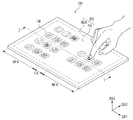
도 2는 도 1에 도시된 표시 장치의 폴딩 상태를 도시한 도면이다.
도 3은 일 실시예에 따른 표시 장치의 사시도이다.
도 4는 도 3에 도시된 표시 장치의 폴딩 상태를 도시한 도면이다.
도 5는 일 실시예에 따른 표시 장치에 대한 분해 사시도이다.
도 6은 일 실시예에 따른 표시 장치의 단면도이다.
도 7은 일 실시예에 따른 광학층의 단면도이다.
도 8은 일 실시예에 따른 광학층을 단면도이다.
도 9는 일 실시예에 따른 표시 장치의 단면도이다.
도 10은 비교예, 및 실시예에 따른 표시 장치의 반사율을 도시한 그래프이다.
| 구분 | 비교예 | 실시예 |
| 내마모 특성 측정 | 3000회 | 6000회 |
| 내약품 특성 측정 | 1000회 | 3000회 |
WP: 윈도우 패널 DM: 표시 모듈
OPL, OPL1, OPL2: 광학층
FL1: 제1 기능층 FL2: 제2 기능층
GP: 유리 기판 BS: 베이스층
CFL: 컬러필터층
Claims (22)
- 표시 모듈;
상기 표시 모듈 상부에 배치된 컬러필터층; 및
상기 컬러필터층 상부에 배치되고, 상기 컬러필터층에 인접한 유리 기판, 및 상기 유리 기판 상부에 배치되고 반사율이 1.08% 이상 5.00% 이하인 광학층을 포함하는 윈도우 패널을 포함하고,
상기 광학층은
상기 유리 기판에 인접한 베이스층;
상기 베이스층의 상부에 배치되고, 하드코팅제 및 대전방지제를 포함하는 제1 기능층; 및
상기 제1 기능층 상부에 배치되고, 불소 함유 실란 화합물을 포함하는 제2 기능층을 포함하는 표시 장치. - 제1항에 있어서,
상기 제2 기능층은 단일층(single layer)이고,
상기 제2 기능층의 굴절률은 1.3 이상 1.5 이하인 표시 장치. - 제2항에 있어서,
상기 제2 기능층의 두께는 30nm 이상 120nm 이하인 표시 장치. - 제1항에 있어서,
상기 제2 기능층은
상기 제1 기능층에 인접하고, 굴절률이 1.3 이상 1.5 이하이고, 상기 불소 함유 실란 화합물을 미포함하는 제1 서브 기능층; 및
상기 제1 서브 기능층 상부에 배치되고, 상기 불소 함유 실란 화합물을 포함하는 제2 서브 기능층을 포함하는 표시 장치. - 제4항에 있어서,
상기 제1 서브 기능층의 두께는 30nm 이상 120nm 이하이고,
상기 제2 서브 기능층의 두께는 1nm 이상 25nm 이하인 표시 장치. - 제4항에 있어서,
상기 제1 서브 기능층은 실리콘 옥사이드를 포함하는 표시 장치. - 제1항에 있어서,
상기 제2 기능층은
상기 제1 기능층에 인접하며, 교번하여 배치된 적어도 하나의 고굴절층 및 적어도 하나의 저굴절층을 포함하는 제1 서브 기능층; 및
상기 제1 서브 기능층 상부에 배치되고, 상기 불소 함유 실란 화합물을 포함하는 제2 서브 기능층을 포함하는 표시 장치. - 제1항에 있어서,
상기 제2 기능층은
제1 서브 기능층; 및
상기 제1 서브 기능층 상부에 배치되고, 상기 불소 함유 실란 화합물을 포함하는 제2 서브 기능층을 포함하고,
상기 제1 서브 기능층은 상기 제1 기능층에서 상기 제2 서브 기능층 방향으로 순차적으로 적층된 제1 굴절층 내지 제4 굴절층을 포함하고,
상기 제1 굴절층 및 상기 제3 굴절층의 굴절률은 각각 2.0 이상 2.5 이하이고, 상기 제2 굴절층 및 상기 제4 굴절층의 굴절률은 각각 1.3 이상 1.5 이하인 표시 장치. - 제8항에 있어서,
상기 제1 굴절층 및 상기 제3 굴절층은 니오븀 옥사이드를 포함하고,
상기 제2 굴절층 및 상기 제4 굴절층은 실리콘 옥사이드를 포함하는 표시 장치. - 제8항에 있어서,
상기 제1 굴절층의 두께는 10nm 이상 20nm 이하이고,
상기 제2 굴절층의 두께는 20nm 이상 40nm 이하이고,
상기 제3 굴절층의 두께는 100nm 이상 150nm 이하이고,
상기 제4 굴절층의 두께는 50nm 이상 150nm 이하인 표시 장치. - 제10항에 있어서,
상기 제2 서브 기능층의 두께는 1nm 이상 25nm 이하인 표시 장치. - 제1항에 있어서,
상기 베이스층과 상기 제1 기능층 사이에 배치되고, 인듐 옥사이드를 포함하는 충격 흡수층을 더 포함하는 표시 장치. - 제12항에 있어서,
상기 충격 흡수층의 두께는 1nm 이상 10nm 이하인 표시 장치. - 제1항에 있어서,
상기 베이스층은 폴리이미드, 폴리에틸렌테레프탈레이트, 및 폴리카보네이트 중 적어도 하나를 포함하는 표시 장치. - 제1항에 있어서,
상기 베이스층의 모듈러스는 3GPa 이상 5GPa 이하인 표시 장치. - 제1항에 있어서,
상기 표시 장치는 일 방향으로 연장되는 폴딩축을 기준으로 폴딩되는 폴딩 영역, 상기 폴딩 영역을 사이에 두고 서로 이격되어 배치된 제1 비폴딩 영역, 및 제2 비폴딩 영역을 포함하는 표시 장치. - 표시 모듈;
상기 표시 모듈 상부에 배치된 컬러필터층; 및
상기 컬러필터층 상부에 배치되고, 상기 컬러필터층에 인접한 유리 기판, 및 상기 유리 기판 상부에 배치된 광학층을 포함하는 윈도우 패널을 포함하고,
상기 광학층은
상기 유리 기판에 인접한 베이스층;
상기 베이스층의 상부에 배치되고 하드코팅제 및 대전방지제를 포함하는 제1 기능층; 및
상기 제1 기능층 상부에 배치되고, 방오제를 포함하며, 굴절률이 1.3 이상 1.5 이하인 제2 기능층을 포함하는 표시 장치. - 제17항에 있어서,
상기 제2 기능층은 단일층이고,
상기 제2 기능층의 두께는 30nm 이상 120nm 이하인 표시 장치. - 제17항에 있어서,
상기 제2 기능층은
상기 제1 기능층에 인접하고, 상기 방오제를 미포함하고, 굴절률이 1.3 이상 1.5 이하인 제1 서브 기능층; 및
상기 제1 서브 기능층 상에 배치되고, 상기 방오제를 포함하는 제2 서브 기능층을 포함하는 표시 장치. - 제19항에 있어서,
상기 제2 기능층은
상기 제1 서브 기능층과 상기 제1 기능층 사이에 배치되고, 굴절률이 2.0 이상 2.5 이하인 제3 서브 기능층;
상기 제3 서브 기능층과 상기 제1 서브 기능층 사이에 배치되고, 굴절률이 1.3 이상 1.5 이하인 제4 서브 기능층; 및
상기 제4 서브 기능층과 상기 제1 서브 기능층 사이에 배치되고, 굴절률이 2.0 이상 2.5 이하인 제5 서브 기능층을 더 포함하는 표시 장치. - 제17항에 있어서,
상기 광학층의 반사율은 1.08% 이상 5.00% 이하인 표시 장치. - 제17항에 있어서,
평면 상에서 서로 이격된 복수 개의 발광 영역들 및 이웃하는 상기 발광 영역들을 사이에 배치된 비발광 영역을 포함하고,
상기 컬러필터층은
상기 발광 영역에 대응하는 복수 개의 필터부들;
상기 필터부들 사이에 배치되고, 상기 비발광 영역에 대응하는 차광부; 및
상기 필터부들과 상기 차광부를 커버하는 유기층을 포함하는 표시 장치.
Priority Applications (3)
| Application Number | Priority Date | Filing Date | Title |
|---|---|---|---|
| KR1020210053290A KR20220146749A (ko) | 2021-04-23 | 2021-04-23 | 표시 장치 |
| CN202210383303.0A CN115236774A (zh) | 2021-04-23 | 2022-04-13 | 显示装置 |
| US17/726,177 US20220344623A1 (en) | 2021-04-23 | 2022-04-21 | Display device |
Applications Claiming Priority (1)
| Application Number | Priority Date | Filing Date | Title |
|---|---|---|---|
| KR1020210053290A KR20220146749A (ko) | 2021-04-23 | 2021-04-23 | 표시 장치 |
Publications (1)
| Publication Number | Publication Date |
|---|---|
| KR20220146749A true KR20220146749A (ko) | 2022-11-02 |
Family
ID=83667635
Family Applications (1)
| Application Number | Title | Priority Date | Filing Date |
|---|---|---|---|
| KR1020210053290A Ceased KR20220146749A (ko) | 2021-04-23 | 2021-04-23 | 표시 장치 |
Country Status (3)
| Country | Link |
|---|---|
| US (1) | US20220344623A1 (ko) |
| KR (1) | KR20220146749A (ko) |
| CN (1) | CN115236774A (ko) |
Family Cites Families (2)
| Publication number | Priority date | Publication date | Assignee | Title |
|---|---|---|---|---|
| JP3569538B2 (ja) * | 1993-12-27 | 2004-09-22 | 松下電器産業株式会社 | 画像表示装置 |
| KR102822477B1 (ko) * | 2019-02-11 | 2025-06-20 | 삼성디스플레이 주식회사 | 표시 장치 |
-
2021
- 2021-04-23 KR KR1020210053290A patent/KR20220146749A/ko not_active Ceased
-
2022
- 2022-04-13 CN CN202210383303.0A patent/CN115236774A/zh active Pending
- 2022-04-21 US US17/726,177 patent/US20220344623A1/en active Pending
Also Published As
| Publication number | Publication date |
|---|---|
| CN115236774A (zh) | 2022-10-25 |
| US20220344623A1 (en) | 2022-10-27 |
Similar Documents
| Publication | Publication Date | Title |
|---|---|---|
| CN109388292B (zh) | 显示装置 | |
| KR102731992B1 (ko) | 유기 발광 표시 장치 | |
| US10971557B2 (en) | Display device having color filter with scattering agent | |
| US12302695B2 (en) | Display device | |
| KR20220096755A (ko) | 폴더블 표시 장치 | |
| KR20220086771A (ko) | 표시 장치와 그의 제조 방법 | |
| EP3796626A1 (en) | Display screen and terminal | |
| US20250284312A1 (en) | Electronic device | |
| US20220147170A1 (en) | Display device | |
| US20210257582A1 (en) | Display device | |
| KR20250052322A (ko) | 보호필름 및 이를 포함하는 표시장치 | |
| US20250280709A1 (en) | Foldable display device | |
| KR20220146749A (ko) | 표시 장치 | |
| KR20220125874A (ko) | 윈도우 제조 장치, 윈도우 제조 방법 및 표시장치 제조 방법 | |
| KR20240036757A (ko) | 표시 장치 | |
| US20240284769A1 (en) | Display device | |
| KR20240111852A (ko) | 윈도우 및 이를 포함하는 표시장치 | |
| US20240389438A1 (en) | Window and display device including the same | |
| US20240244940A1 (en) | Protection film and display device including the same | |
| US12307998B2 (en) | Window and display device including the same | |
| KR20240149491A (ko) | 표시 장치 및 이의 제조 방법 | |
| KR20250031124A (ko) | 발광 표시 장치 | |
| KR20260003442A (ko) | 윈도우 및 이를 포함하는 표시 장치 | |
| US20250228104A1 (en) | Display device and method for manufacturing the display device | |
| KR20260018217A (ko) | 윈도우 및 이를 포함하는 전자 장치 |
Legal Events
| Date | Code | Title | Description |
|---|---|---|---|
| PA0109 | Patent application |
St.27 status event code: A-0-1-A10-A12-nap-PA0109 |
|
| PG1501 | Laying open of application |
St.27 status event code: A-1-1-Q10-Q12-nap-PG1501 |
|
| P22-X000 | Classification modified |
St.27 status event code: A-2-2-P10-P22-nap-X000 |
|
| P22-X000 | Classification modified |
St.27 status event code: A-2-2-P10-P22-nap-X000 |
|
| A201 | Request for examination | ||
| PA0201 | Request for examination |
St.27 status event code: A-1-2-D10-D11-exm-PA0201 |
|
| D13-X000 | Search requested |
St.27 status event code: A-1-2-D10-D13-srh-X000 |
|
| D14-X000 | Search report completed |
St.27 status event code: A-1-2-D10-D14-srh-X000 |
|
| E902 | Notification of reason for refusal | ||
| PE0902 | Notice of grounds for rejection |
St.27 status event code: A-1-2-D10-D21-exm-PE0902 |
|
| P11-X000 | Amendment of application requested |
St.27 status event code: A-2-2-P10-P11-nap-X000 |
|
| P13-X000 | Application amended |
St.27 status event code: A-2-2-P10-P13-nap-X000 |
|
| B15 | Application refused following examination |
Free format text: ST27 STATUS EVENT CODE: N-2-6-B10-B15-EXM-PE0601 (AS PROVIDED BY THE NATIONAL OFFICE) |
|
| PE0601 | Decision on rejection of patent |
St.27 status event code: N-2-6-B10-B15-exm-PE0601 |
|
| E13 | Pre-grant limitation requested |
Free format text: ST27 STATUS EVENT CODE: A-2-3-E10-E13-LIM-X000 (AS PROVIDED BY THE NATIONAL OFFICE) |
|
| E13-X000 | Pre-grant limitation requested |
St.27 status event code: A-2-3-E10-E13-lim-X000 |
|
| P11 | Amendment of application requested |
Free format text: ST27 STATUS EVENT CODE: A-2-2-P10-P11-NAP-X000 (AS PROVIDED BY THE NATIONAL OFFICE) |
|
| P11-X000 | Amendment of application requested |
St.27 status event code: A-2-2-P10-P11-nap-X000 |
|
| P22-X000 | Classification modified |
St.27 status event code: A-2-2-P10-P22-nap-X000 |