KR20220163461A - 타겟 배열을 포함하는 기판, 및 연관된 적어도 하나의 패터닝 디바이스, 리소그래피 방법 및 계측 방법 - Google Patents
타겟 배열을 포함하는 기판, 및 연관된 적어도 하나의 패터닝 디바이스, 리소그래피 방법 및 계측 방법 Download PDFInfo
- Publication number
- KR20220163461A KR20220163461A KR1020227038552A KR20227038552A KR20220163461A KR 20220163461 A KR20220163461 A KR 20220163461A KR 1020227038552 A KR1020227038552 A KR 1020227038552A KR 20227038552 A KR20227038552 A KR 20227038552A KR 20220163461 A KR20220163461 A KR 20220163461A
- Authority
- KR
- South Korea
- Prior art keywords
- target
- substrate
- metrology
- pair
- array
- Prior art date
- Legal status (The legal status is an assumption and is not a legal conclusion. Google has not performed a legal analysis and makes no representation as to the accuracy of the status listed.)
- Granted
Links
Images





Classifications
-
- G—PHYSICS
- G03—PHOTOGRAPHY; CINEMATOGRAPHY; ANALOGOUS TECHNIQUES USING WAVES OTHER THAN OPTICAL WAVES; ELECTROGRAPHY; HOLOGRAPHY
- G03F—PHOTOMECHANICAL PRODUCTION OF TEXTURED OR PATTERNED SURFACES, e.g. FOR PRINTING, FOR PROCESSING OF SEMICONDUCTOR DEVICES; MATERIALS THEREFOR; ORIGINALS THEREFOR; APPARATUS SPECIALLY ADAPTED THEREFOR
- G03F7/00—Photomechanical, e.g. photolithographic, production of textured or patterned surfaces, e.g. printing surfaces; Materials therefor, e.g. comprising photoresists; Apparatus specially adapted therefor
- G03F7/70—Microphotolithographic exposure; Apparatus therefor
- G03F7/70483—Information management; Active and passive control; Testing; Wafer monitoring, e.g. pattern monitoring
- G03F7/70605—Workpiece metrology
- G03F7/70681—Metrology strategies
- G03F7/70683—Mark designs
-
- G—PHYSICS
- G03—PHOTOGRAPHY; CINEMATOGRAPHY; ANALOGOUS TECHNIQUES USING WAVES OTHER THAN OPTICAL WAVES; ELECTROGRAPHY; HOLOGRAPHY
- G03F—PHOTOMECHANICAL PRODUCTION OF TEXTURED OR PATTERNED SURFACES, e.g. FOR PRINTING, FOR PROCESSING OF SEMICONDUCTOR DEVICES; MATERIALS THEREFOR; ORIGINALS THEREFOR; APPARATUS SPECIALLY ADAPTED THEREFOR
- G03F7/00—Photomechanical, e.g. photolithographic, production of textured or patterned surfaces, e.g. printing surfaces; Materials therefor, e.g. comprising photoresists; Apparatus specially adapted therefor
- G03F7/70—Microphotolithographic exposure; Apparatus therefor
- G03F7/70483—Information management; Active and passive control; Testing; Wafer monitoring, e.g. pattern monitoring
- G03F7/70605—Workpiece metrology
- G03F7/70616—Monitoring the printed patterns
- G03F7/70641—Focus
-
- G—PHYSICS
- G01—MEASURING; TESTING
- G01N—INVESTIGATING OR ANALYSING MATERIALS BY DETERMINING THEIR CHEMICAL OR PHYSICAL PROPERTIES
- G01N21/00—Investigating or analysing materials by the use of optical means, i.e. using sub-millimetre waves, infrared, visible or ultraviolet light
- G01N21/17—Systems in which incident light is modified in accordance with the properties of the material investigated
- G01N21/47—Scattering, i.e. diffuse reflection
- G01N21/4788—Diffraction
-
- G—PHYSICS
- G01—MEASURING; TESTING
- G01N—INVESTIGATING OR ANALYSING MATERIALS BY DETERMINING THEIR CHEMICAL OR PHYSICAL PROPERTIES
- G01N21/00—Investigating or analysing materials by the use of optical means, i.e. using sub-millimetre waves, infrared, visible or ultraviolet light
- G01N21/84—Systems specially adapted for particular applications
- G01N21/88—Investigating the presence of flaws or contamination
- G01N21/95—Investigating the presence of flaws or contamination characterised by the material or shape of the object to be examined
- G01N21/9501—Semiconductor wafers
-
- G—PHYSICS
- G01—MEASURING; TESTING
- G01N—INVESTIGATING OR ANALYSING MATERIALS BY DETERMINING THEIR CHEMICAL OR PHYSICAL PROPERTIES
- G01N21/00—Investigating or analysing materials by the use of optical means, i.e. using sub-millimetre waves, infrared, visible or ultraviolet light
- G01N21/84—Systems specially adapted for particular applications
- G01N21/88—Investigating the presence of flaws or contamination
- G01N21/95—Investigating the presence of flaws or contamination characterised by the material or shape of the object to be examined
- G01N21/956—Inspecting patterns on the surface of objects
-
- G—PHYSICS
- G03—PHOTOGRAPHY; CINEMATOGRAPHY; ANALOGOUS TECHNIQUES USING WAVES OTHER THAN OPTICAL WAVES; ELECTROGRAPHY; HOLOGRAPHY
- G03F—PHOTOMECHANICAL PRODUCTION OF TEXTURED OR PATTERNED SURFACES, e.g. FOR PRINTING, FOR PROCESSING OF SEMICONDUCTOR DEVICES; MATERIALS THEREFOR; ORIGINALS THEREFOR; APPARATUS SPECIALLY ADAPTED THEREFOR
- G03F1/00—Originals for photomechanical production of textured or patterned surfaces, e.g., masks, photo-masks, reticles; Mask blanks or pellicles therefor; Containers specially adapted therefor; Preparation thereof
- G03F1/38—Masks having auxiliary features, e.g. special coatings or marks for alignment or testing; Preparation thereof
- G03F1/42—Alignment or registration features, e.g. alignment marks on the mask substrates
-
- G—PHYSICS
- G03—PHOTOGRAPHY; CINEMATOGRAPHY; ANALOGOUS TECHNIQUES USING WAVES OTHER THAN OPTICAL WAVES; ELECTROGRAPHY; HOLOGRAPHY
- G03F—PHOTOMECHANICAL PRODUCTION OF TEXTURED OR PATTERNED SURFACES, e.g. FOR PRINTING, FOR PROCESSING OF SEMICONDUCTOR DEVICES; MATERIALS THEREFOR; ORIGINALS THEREFOR; APPARATUS SPECIALLY ADAPTED THEREFOR
- G03F7/00—Photomechanical, e.g. photolithographic, production of textured or patterned surfaces, e.g. printing surfaces; Materials therefor, e.g. comprising photoresists; Apparatus specially adapted therefor
- G03F7/70—Microphotolithographic exposure; Apparatus therefor
- G03F7/70483—Information management; Active and passive control; Testing; Wafer monitoring, e.g. pattern monitoring
- G03F7/7055—Exposure light control in all parts of the microlithographic apparatus, e.g. pulse length control or light interruption
- G03F7/70558—Dose control, i.e. achievement of a desired dose
-
- G—PHYSICS
- G03—PHOTOGRAPHY; CINEMATOGRAPHY; ANALOGOUS TECHNIQUES USING WAVES OTHER THAN OPTICAL WAVES; ELECTROGRAPHY; HOLOGRAPHY
- G03F—PHOTOMECHANICAL PRODUCTION OF TEXTURED OR PATTERNED SURFACES, e.g. FOR PRINTING, FOR PROCESSING OF SEMICONDUCTOR DEVICES; MATERIALS THEREFOR; ORIGINALS THEREFOR; APPARATUS SPECIALLY ADAPTED THEREFOR
- G03F7/00—Photomechanical, e.g. photolithographic, production of textured or patterned surfaces, e.g. printing surfaces; Materials therefor, e.g. comprising photoresists; Apparatus specially adapted therefor
- G03F7/70—Microphotolithographic exposure; Apparatus therefor
- G03F7/70483—Information management; Active and passive control; Testing; Wafer monitoring, e.g. pattern monitoring
- G03F7/70605—Workpiece metrology
- G03F7/70616—Monitoring the printed patterns
- G03F7/70625—Dimensions, e.g. line width, critical dimension [CD], profile, sidewall angle or edge roughness
-
- G—PHYSICS
- G03—PHOTOGRAPHY; CINEMATOGRAPHY; ANALOGOUS TECHNIQUES USING WAVES OTHER THAN OPTICAL WAVES; ELECTROGRAPHY; HOLOGRAPHY
- G03F—PHOTOMECHANICAL PRODUCTION OF TEXTURED OR PATTERNED SURFACES, e.g. FOR PRINTING, FOR PROCESSING OF SEMICONDUCTOR DEVICES; MATERIALS THEREFOR; ORIGINALS THEREFOR; APPARATUS SPECIALLY ADAPTED THEREFOR
- G03F7/00—Photomechanical, e.g. photolithographic, production of textured or patterned surfaces, e.g. printing surfaces; Materials therefor, e.g. comprising photoresists; Apparatus specially adapted therefor
- G03F7/70—Microphotolithographic exposure; Apparatus therefor
- G03F7/70483—Information management; Active and passive control; Testing; Wafer monitoring, e.g. pattern monitoring
- G03F7/70605—Workpiece metrology
- G03F7/70616—Monitoring the printed patterns
- G03F7/70633—Overlay, i.e. relative alignment between patterns printed by separate exposures in different layers, or in the same layer in multiple exposures or stitching
-
- G—PHYSICS
- G03—PHOTOGRAPHY; CINEMATOGRAPHY; ANALOGOUS TECHNIQUES USING WAVES OTHER THAN OPTICAL WAVES; ELECTROGRAPHY; HOLOGRAPHY
- G03F—PHOTOMECHANICAL PRODUCTION OF TEXTURED OR PATTERNED SURFACES, e.g. FOR PRINTING, FOR PROCESSING OF SEMICONDUCTOR DEVICES; MATERIALS THEREFOR; ORIGINALS THEREFOR; APPARATUS SPECIALLY ADAPTED THEREFOR
- G03F7/00—Photomechanical, e.g. photolithographic, production of textured or patterned surfaces, e.g. printing surfaces; Materials therefor, e.g. comprising photoresists; Apparatus specially adapted therefor
- G03F7/70—Microphotolithographic exposure; Apparatus therefor
- G03F7/70483—Information management; Active and passive control; Testing; Wafer monitoring, e.g. pattern monitoring
- G03F7/70605—Workpiece metrology
- G03F7/706843—Metrology apparatus
- G03F7/706847—Production of measurement radiation, e.g. synchrotron, free-electron laser, plasma source or higher harmonic generation [HHG]
-
- G—PHYSICS
- G03—PHOTOGRAPHY; CINEMATOGRAPHY; ANALOGOUS TECHNIQUES USING WAVES OTHER THAN OPTICAL WAVES; ELECTROGRAPHY; HOLOGRAPHY
- G03F—PHOTOMECHANICAL PRODUCTION OF TEXTURED OR PATTERNED SURFACES, e.g. FOR PRINTING, FOR PROCESSING OF SEMICONDUCTOR DEVICES; MATERIALS THEREFOR; ORIGINALS THEREFOR; APPARATUS SPECIALLY ADAPTED THEREFOR
- G03F9/00—Registration or positioning of originals, masks, frames, photographic sheets or textured or patterned surfaces, e.g. automatically
- G03F9/70—Registration or positioning of originals, masks, frames, photographic sheets or textured or patterned surfaces, e.g. automatically for microlithography
- G03F9/7003—Alignment type or strategy, e.g. leveling, global alignment
- G03F9/7023—Aligning or positioning in direction perpendicular to substrate surface
- G03F9/7026—Focusing
-
- G—PHYSICS
- G03—PHOTOGRAPHY; CINEMATOGRAPHY; ANALOGOUS TECHNIQUES USING WAVES OTHER THAN OPTICAL WAVES; ELECTROGRAPHY; HOLOGRAPHY
- G03F—PHOTOMECHANICAL PRODUCTION OF TEXTURED OR PATTERNED SURFACES, e.g. FOR PRINTING, FOR PROCESSING OF SEMICONDUCTOR DEVICES; MATERIALS THEREFOR; ORIGINALS THEREFOR; APPARATUS SPECIALLY ADAPTED THEREFOR
- G03F9/00—Registration or positioning of originals, masks, frames, photographic sheets or textured or patterned surfaces, e.g. automatically
- G03F9/70—Registration or positioning of originals, masks, frames, photographic sheets or textured or patterned surfaces, e.g. automatically for microlithography
- G03F9/7073—Alignment marks and their environment
- G03F9/7076—Mark details, e.g. phase grating mark, temporary mark
-
- H01L22/34—
-
- H—ELECTRICITY
- H10—SEMICONDUCTOR DEVICES; ELECTRIC SOLID-STATE DEVICES NOT OTHERWISE PROVIDED FOR
- H10P—GENERIC PROCESSES OR APPARATUS FOR THE MANUFACTURE OR TREATMENT OF DEVICES COVERED BY CLASS H10
- H10P74/00—Testing or measuring during manufacture or treatment of wafers, substrates or devices
- H10P74/27—Structural arrangements therefor
- H10P74/277—Circuits for electrically characterising or monitoring manufacturing processes, e.g. circuits in tested chips or circuits in testing wafers
Landscapes
- Physics & Mathematics (AREA)
- General Physics & Mathematics (AREA)
- Pathology (AREA)
- Immunology (AREA)
- General Health & Medical Sciences (AREA)
- Health & Medical Sciences (AREA)
- Life Sciences & Earth Sciences (AREA)
- Chemical & Material Sciences (AREA)
- Analytical Chemistry (AREA)
- Biochemistry (AREA)
- Engineering & Computer Science (AREA)
- Plasma & Fusion (AREA)
- Optics & Photonics (AREA)
- Exposure And Positioning Against Photoresist Photosensitive Materials (AREA)
- Automation & Control Theory (AREA)
- Manufacturing & Machinery (AREA)
- Length-Measuring Devices Using Wave Or Particle Radiation (AREA)
- Analysing Materials By The Use Of Radiation (AREA)
- Exposure Of Semiconductors, Excluding Electron Or Ion Beam Exposure (AREA)
Abstract
Description
도 1은 본 발명의 일 실시예에 따른 리소그래피 장치를 나타낸다.
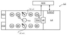
도 2은 본 발명의 일 실시예에 따른 리소그래피 셀 또는 클러스터를 나타낸다.
도 3은 (a) 제1 쌍의 조명 개구를 이용하여 타겟을 측정하는 데 사용하기 위한 암시야 스케터로미터의 개략도; (b) 주어진 조명 방향에 대한 타겟 격자의 회절 스펙트럼의 세부 사항; (c) 회절 기반 오버레이 측정을 위해 스캐터로미터를 이용함에 있어서 추가적인 조명 모드를 제공하는 제2 쌍의 조명 개구; 및 (d) 제1 쌍 및 제2 쌍의 개구를 조합한 제3 쌍의 조명 개구를 나타낸다.
도 4은 다중 격자 타겟의 공지된 형태 및 기판 상의 측정 스폿의 개요를 나타낸 것이다.
도 5는 도 3의 스캐터로미터에서 획득한 도 4의 타겟의 이미지를 나타낸다.
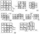
도 6(a)-(h)는 본 발명의 실시예에 따른 타겟 배열의 예를 개략적으로 나타낸 것이다;
도 7(a) 및 (b)는 본 발명의 일 실시예에 따라 중심대칭인 타겟 영역들이 비-중심대칭인 배열로부터 어떻게 추출될 수 있는지를 나타낸다.
도 8(a) 및 (b)는 본 발명의 일 실시예에 따른 타겟 배열의 두 가지 측정 구성을 예시한다.










Claims (14)
- 리소그래피 프로세스의 계측에 적합한 적어도 하나의 타겟 배열을 포함하는 기판으로서, 타겟 배열은 적어도 한 쌍의 유사한 타겟 영역들을 포함하되, 적어도 한 쌍의 유사한 타겟 영역들은 타겟 배열이 중심대칭(centrosymmetric)이 되거나 또는 적어도 단일 방향으로 함께 측정하기 위한 타겟 영역들이 중심대칭이 되도록 배열되는, 기판.
- 제1항에 있어서,
상기 타겟 배열은, 상기 적어도 한 쌍의 유사한 타겟 영역들이, 또는 적어도 단일 방향으로 측정하기 위한 그러한 타겟 영역들이, 중심대칭점 주위로 180도 회전될 때 계측 장치에 동일하게 보이게 되도록 하는 것인, 기판. - 제1항 또는 제2항에 있어서,
상기 적어도 한 쌍의 유사한 타겟 영역들은 적어도 제1 쌍의 유사한 타겟 영역들 및 제2 쌍의 유사한 타겟 영역들을 포함하는, 기판. - 제3항에 있어서,
상기 제1 쌍의 유사한 타겟 영역들은 제1 유형의 타겟 영역들을 포함하고 상기 제2 쌍의 유사한 타겟 영역들은 제2 유형의 타겟 영역들을 포함하는, 기판. - 제4항에 있어서,
상기 제1 유형의 타겟 영역들은 제1 피치를 갖는 제1 층의 주기적 구조체 및 제2 피치를 갖는 제2 층의 주기적 구조체를 포함하고, 상기 제2 유형의 타겟 영역들은 제2 피치를 갖는 제1 층의 주기적 구조체 및 제1 피치를 갖는 제2 층의 주기적 구조체를 포함하는, 기판. - 제1항 내지 제5항 중 어느 한 항에 있어서,
상기 적어도 한 쌍의 타겟 영역들은 2개의 직교 방향으로 계측을 수행하기 위해 측정 방향마다 적어도 한 쌍의 타겟 영역들을 포함하는, 기판. - 제1항 내지 제6항 중 어느 한 항에 있어서,
상기 타겟 배열은 각각의 측정 방향의 타겟 영역들에 대해 공통된 중심대칭점을 갖는, 기판. - 제1항 내지 제7항 중 어느 한 항에 있어서,
상기 타겟 배열은 중심대칭인, 기판. - 제1항 내지 제6항 중 어느 한 항에 있어서,
상기 타겟 배열은 각각의 측정 방향의 타겟 영역들에 대해 별개의 중심대칭점을 갖는, 기판. - 제9항에 있어서,
상기 타겟 배열은 측정 방향마다 중심대칭인, 기판. - 제1항 내지 제10항 중 어느 한 항에 있어서,
각각의 상기 타겟 영역들은 별개의 타겟 구조체를 포함하는, 기판. - 제1항 내지 제10항 중 어느 한 항에 있어서,
상기 타겟 영역들의 적어도 일부는 더 큰 타겟 구조체의 일부를 포함하는, 기판. - 제1항 내지 제12항 중 어느 한 항에 있어서,
상기 타겟 배열은 오버레이, 포커스, 선량 및 기판 상에 존재하는 디바이스 구조체에 관련된 물리적 파라미터 중 하나 이상을 측정하기에 적합한 것인, 기판. - 제1항 내지 제13항 중 어느 한 항에 있어서,
상기 타겟 배열은 이미지 기반 계측 및/또는 회절 기반 계측에 적합한 것인, 기판.
Applications Claiming Priority (5)
| Application Number | Priority Date | Filing Date | Title |
|---|---|---|---|
| EP20173476 | 2020-05-07 | ||
| EP20173476.1 | 2020-05-07 | ||
| EP20182160 | 2020-06-25 | ||
| EP20182160.0 | 2020-06-25 | ||
| PCT/EP2021/060403 WO2021224009A1 (en) | 2020-05-07 | 2021-04-21 | A substrate comprising a target arrangement, and associated at least one patterning device, lithographic method and metrology method |
Publications (2)
| Publication Number | Publication Date |
|---|---|
| KR20220163461A true KR20220163461A (ko) | 2022-12-09 |
| KR102874820B1 KR102874820B1 (ko) | 2025-10-21 |
Family
ID=75625585
Family Applications (1)
| Application Number | Title | Priority Date | Filing Date |
|---|---|---|---|
| KR1020227038552A Active KR102874820B1 (ko) | 2020-05-07 | 2021-04-21 | 타겟 배열을 포함하는 기판, 및 연관된 적어도 하나의 패터닝 디바이스, 리소그래피 방법 및 계측 방법 |
Country Status (6)
| Country | Link |
|---|---|
| US (1) | US12276921B2 (ko) |
| KR (1) | KR102874820B1 (ko) |
| CN (1) | CN115552221B (ko) |
| IL (1) | IL297343A (ko) |
| TW (2) | TWI793593B (ko) |
| WO (1) | WO2021224009A1 (ko) |
Families Citing this family (4)
| Publication number | Priority date | Publication date | Assignee | Title |
|---|---|---|---|---|
| EP4191338A1 (en) * | 2021-12-03 | 2023-06-07 | ASML Netherlands B.V. | Metrology calibration method |
| EP4224255A1 (en) | 2022-02-08 | 2023-08-09 | ASML Netherlands B.V. | Metrology method |
| US12601979B2 (en) * | 2023-09-15 | 2026-04-14 | Kla Corporation | Multi-column large field of view imaging platform |
| WO2025131461A1 (en) * | 2023-12-20 | 2025-06-26 | Asml Netherlands B.V. | Non-centrosymmetric fringe-based metrology targets and methods |
Citations (4)
| Publication number | Priority date | Publication date | Assignee | Title |
|---|---|---|---|---|
| US20070229829A1 (en) * | 2006-03-31 | 2007-10-04 | Kla-Tencor Technologies Corporation | Apparatus and methods for detecting overlay errors using scatterometry |
| KR20130088848A (ko) * | 2010-08-03 | 2013-08-08 | 케이엘에이-텐코 코포레이션 | 다층 오버레이 계측 타겟 및 상보적 오버레이 계측 측정 시스템 |
| KR20170048489A (ko) * | 2014-08-29 | 2017-05-08 | 에이에스엠엘 네델란즈 비.브이. | 메트롤로지 방법, 타겟 및 기판 |
| WO2020074412A1 (en) * | 2018-10-08 | 2020-04-16 | Asml Netherlands B.V. | Metrology method, patterning device, apparatus and computer program |
Family Cites Families (24)
| Publication number | Priority date | Publication date | Assignee | Title |
|---|---|---|---|---|
| US7046361B1 (en) * | 2002-04-04 | 2006-05-16 | Nanometrics Incorporated | Positioning two elements using an alignment target with a designed offset |
| US20060012779A1 (en) * | 2004-07-13 | 2006-01-19 | Asml Netherlands B.V. | Lithographic apparatus and device manufacturing method |
| US7724370B2 (en) * | 2007-03-01 | 2010-05-25 | Asml Netherlands B.V. | Method of inspection, a method of manufacturing, an inspection apparatus, a substrate, a mask, a lithography apparatus and a lithographic cell |
| US7605907B2 (en) | 2007-03-27 | 2009-10-20 | Asml Netherlands B.V. | Method of forming a substrate for use in calibrating a metrology tool, calibration substrate and metrology tool calibration method |
| NL1036245A1 (nl) | 2007-12-17 | 2009-06-18 | Asml Netherlands Bv | Diffraction based overlay metrology tool and method of diffraction based overlay metrology. |
| NL1036597A1 (nl) | 2008-02-29 | 2009-09-01 | Asml Netherlands Bv | Metrology method and apparatus, lithographic apparatus, and device manufacturing method. |
| NL1036857A1 (nl) | 2008-04-21 | 2009-10-22 | Asml Netherlands Bv | Inspection method and apparatus, lithographic apparatus, lithographic processing cell and device manufacturing method. |
| NL2004094A (en) | 2009-02-11 | 2010-08-12 | Asml Netherlands Bv | Inspection apparatus, lithographic apparatus, lithographic processing cell and inspection method. |
| JP5545782B2 (ja) | 2009-07-31 | 2014-07-09 | エーエスエムエル ネザーランズ ビー.ブイ. | リソグラフィ装置の焦点測定方法、散乱計、リソグラフィシステム、およびリソグラフィセル |
| KR20120058572A (ko) | 2009-08-24 | 2012-06-07 | 에이에스엠엘 네델란즈 비.브이. | 메트롤로지 방법 및 장치, 리소그래피 장치, 리소그래피 처리 셀 및 메트롤로지 타겟들을 포함하는 기판 |
| WO2012022584A1 (en) * | 2010-08-18 | 2012-02-23 | Asml Netherlands B.V. | Substrate for use in metrology, metrology method and device manufacturing method |
| NL2007425A (en) | 2010-11-12 | 2012-05-15 | Asml Netherlands Bv | Metrology method and apparatus, and device manufacturing method. |
| CN103748515A (zh) * | 2011-08-23 | 2014-04-23 | Asml荷兰有限公司 | 量测方法和设备以及器件制造方法 |
| NL2009508A (en) * | 2011-10-24 | 2013-04-25 | Asml Netherlands Bv | Metrology method and apparatus, and device manufacturing method. |
| US9535338B2 (en) * | 2012-05-29 | 2017-01-03 | Asml Netherlands B.V. | Metrology method and apparatus, substrate, lithographic system and device manufacturing method |
| WO2015124397A1 (en) * | 2014-02-21 | 2015-08-27 | Asml Netherlands B.V. | Optimization of target arrangement and associated target |
| NL2017300A (en) * | 2015-08-27 | 2017-03-01 | Asml Netherlands Bv | Method and apparatus for measuring a parameter of a lithographic process, substrate and patterning devices for use in the method |
| KR20200004381A (ko) | 2017-05-08 | 2020-01-13 | 에이에스엠엘 네델란즈 비.브이. | 구조체를 측정하는 방법, 검사 장치, 리소그래피 시스템 및 디바이스 제조 방법 |
| EP3422103A1 (en) * | 2017-06-26 | 2019-01-02 | ASML Netherlands B.V. | Method of determining a performance parameter of a process |
| KR102648880B1 (ko) * | 2017-11-07 | 2024-03-15 | 에이에스엠엘 네델란즈 비.브이. | 관심 특성을 결정하는 계측 장치 및 방법 |
| EP3499312A1 (en) | 2017-12-15 | 2019-06-19 | ASML Netherlands B.V. | Metrology apparatus and a method of determining a characteristic of interest |
| JP7186531B2 (ja) * | 2018-07-13 | 2022-12-09 | キヤノン株式会社 | 露光装置、および物品製造方法 |
| EP3611567A3 (en) | 2019-07-23 | 2020-05-13 | ASML Netherlands B.V. | Improvements in metrology targets |
| EP4202552B1 (en) * | 2021-12-24 | 2024-04-17 | Imec VZW | Method and structure for determining an overlay error |
-
2021
- 2021-04-21 US US17/923,913 patent/US12276921B2/en active Active
- 2021-04-21 KR KR1020227038552A patent/KR102874820B1/ko active Active
- 2021-04-21 WO PCT/EP2021/060403 patent/WO2021224009A1/en not_active Ceased
- 2021-04-21 CN CN202180033275.3A patent/CN115552221B/zh active Active
- 2021-04-21 IL IL297343A patent/IL297343A/en unknown
- 2021-05-07 TW TW110116529A patent/TWI793593B/zh active
- 2021-05-07 TW TW112102551A patent/TWI890022B/zh active
Patent Citations (4)
| Publication number | Priority date | Publication date | Assignee | Title |
|---|---|---|---|---|
| US20070229829A1 (en) * | 2006-03-31 | 2007-10-04 | Kla-Tencor Technologies Corporation | Apparatus and methods for detecting overlay errors using scatterometry |
| KR20130088848A (ko) * | 2010-08-03 | 2013-08-08 | 케이엘에이-텐코 코포레이션 | 다층 오버레이 계측 타겟 및 상보적 오버레이 계측 측정 시스템 |
| KR20170048489A (ko) * | 2014-08-29 | 2017-05-08 | 에이에스엠엘 네델란즈 비.브이. | 메트롤로지 방법, 타겟 및 기판 |
| WO2020074412A1 (en) * | 2018-10-08 | 2020-04-16 | Asml Netherlands B.V. | Metrology method, patterning device, apparatus and computer program |
Also Published As
| Publication number | Publication date |
|---|---|
| KR102874820B1 (ko) | 2025-10-21 |
| WO2021224009A1 (en) | 2021-11-11 |
| TW202331425A (zh) | 2023-08-01 |
| US20230176491A1 (en) | 2023-06-08 |
| US12276921B2 (en) | 2025-04-15 |
| CN115552221A (zh) | 2022-12-30 |
| IL297343A (en) | 2022-12-01 |
| TWI793593B (zh) | 2023-02-21 |
| CN115552221B (zh) | 2025-10-17 |
| TW202147041A (zh) | 2021-12-16 |
| TWI890022B (zh) | 2025-07-11 |
Similar Documents
| Publication | Publication Date | Title |
|---|---|---|
| KR102104843B1 (ko) | 계측 방법 및 장치, 컴퓨터 프로그램 및 리소그래피 시스템 | |
| KR102015934B1 (ko) | 리소그래피를 위한 계측법 | |
| JP6077647B2 (ja) | メトロロジー方法及び装置、基板、リソグラフィシステム並びにデバイス製造方法 | |
| JP6251386B2 (ja) | クリティカルディメンション関連特性を決定する方法、検査装置およびデバイス製造方法 | |
| KR102025214B1 (ko) | 계측 방법 및 장치, 컴퓨터 프로그램 및 리소그래피 시스템 | |
| KR102128523B1 (ko) | 위치 측정 방법, 리소그래피 장치, 리소 셀 및 디바이스 제조 방법 | |
| KR102616712B1 (ko) | 계측 방법, 패터닝 디바이스, 장치 및 컴퓨터 프로그램 | |
| KR102874820B1 (ko) | 타겟 배열을 포함하는 기판, 및 연관된 적어도 하나의 패터닝 디바이스, 리소그래피 방법 및 계측 방법 | |
| WO2020126266A1 (en) | Method of measuring a parameter of a patterning process, metrology apparatus, target | |
| KR102669792B1 (ko) | 리소그래피 프로세스의 파라미터를 측정하기 위한 타겟 | |
| KR102525482B1 (ko) | 계측 방법, 장치 및 컴퓨터 프로그램 | |
| US20240036480A1 (en) | A substrate comprising a target arrangement, and associated at least one patterning device, lithographic method and metrology method | |
| KR20190134804A (ko) | 타겟 측정 방법, 계측 장치, 리소그래피 셀 및 타겟 | |
| CN115698865B (zh) | 用于测量光刻过程的参数的目标 | |
| EP4600737A2 (en) | A substrate, lithographic method and metrology method | |
| US20250060661A1 (en) | Substrate comprising a target arrangement, associated patterning device and metrology method |
Legal Events
| Date | Code | Title | Description |
|---|---|---|---|
| P11-X000 | Amendment of application requested |
St.27 status event code: A-2-2-P10-P11-nap-X000 |
|
| P13-X000 | Application amended |
St.27 status event code: A-2-2-P10-P13-nap-X000 |
|
| PA0105 | International application |
St.27 status event code: A-0-1-A10-A15-nap-PA0105 |
|
| PA0201 | Request for examination |
St.27 status event code: A-1-2-D10-D11-exm-PA0201 |
|
| PG1501 | Laying open of application |
St.27 status event code: A-1-1-Q10-Q12-nap-PG1501 |
|
| P22-X000 | Classification modified |
St.27 status event code: A-2-2-P10-P22-nap-X000 |
|
| D13-X000 | Search requested |
St.27 status event code: A-1-2-D10-D13-srh-X000 |
|
| E902 | Notification of reason for refusal | ||
| PE0902 | Notice of grounds for rejection |
St.27 status event code: A-1-2-D10-D21-exm-PE0902 |
|
| E13-X000 | Pre-grant limitation requested |
St.27 status event code: A-2-3-E10-E13-lim-X000 |
|
| P11-X000 | Amendment of application requested |
St.27 status event code: A-2-2-P10-P11-nap-X000 |
|
| P13-X000 | Application amended |
St.27 status event code: A-2-2-P10-P13-nap-X000 |
|
| D22 | Grant of ip right intended |
Free format text: ST27 STATUS EVENT CODE: A-1-2-D10-D22-EXM-PE0701 (AS PROVIDED BY THE NATIONAL OFFICE) |
|
| PE0701 | Decision of registration |
St.27 status event code: A-1-2-D10-D22-exm-PE0701 |
|
| F11 | Ip right granted following substantive examination |
Free format text: ST27 STATUS EVENT CODE: A-2-4-F10-F11-EXM-PR0701 (AS PROVIDED BY THE NATIONAL OFFICE) |
|
| PR0701 | Registration of establishment |
St.27 status event code: A-2-4-F10-F11-exm-PR0701 |
|
| PR1002 | Payment of registration fee |
St.27 status event code: A-2-2-U10-U12-oth-PR1002 Fee payment year number: 1 |
|
| U12 | Designation fee paid |
Free format text: ST27 STATUS EVENT CODE: A-2-2-U10-U12-OTH-PR1002 (AS PROVIDED BY THE NATIONAL OFFICE) Year of fee payment: 1 |
|
| PG1601 | Publication of registration |
St.27 status event code: A-4-4-Q10-Q13-nap-PG1601 |
|
| Q13 | Ip right document published |
Free format text: ST27 STATUS EVENT CODE: A-4-4-Q10-Q13-NAP-PG1601 (AS PROVIDED BY THE NATIONAL OFFICE) |
|
| P22-X000 | Classification modified |
St.27 status event code: A-4-4-P10-P22-nap-X000 |