KR20220165800A - 표시 장치 및 전자 기기 - Google Patents
표시 장치 및 전자 기기 Download PDFInfo
- Publication number
- KR20220165800A KR20220165800A KR1020227041553A KR20227041553A KR20220165800A KR 20220165800 A KR20220165800 A KR 20220165800A KR 1020227041553 A KR1020227041553 A KR 1020227041553A KR 20227041553 A KR20227041553 A KR 20227041553A KR 20220165800 A KR20220165800 A KR 20220165800A
- Authority
- KR
- South Korea
- Prior art keywords
- transistor
- wiring
- potential
- circuit
- current
- Prior art date
- Legal status (The legal status is an assumption and is not a legal conclusion. Google has not performed a legal analysis and makes no representation as to the accuracy of the status listed.)
- Ceased
Links
- 239000004973 liquid crystal related substance Substances 0.000 claims description 32
- 229910044991 metal oxide Inorganic materials 0.000 claims description 9
- 150000004706 metal oxides Chemical class 0.000 claims description 9
- 230000015572 biosynthetic process Effects 0.000 claims description 6
- 238000012937 correction Methods 0.000 abstract description 64
- 230000008878 coupling Effects 0.000 abstract description 14
- 238000010168 coupling process Methods 0.000 abstract description 14
- 238000005859 coupling reaction Methods 0.000 abstract description 14
- 238000006243 chemical reaction Methods 0.000 abstract description 7
- 238000012545 processing Methods 0.000 abstract description 6
- 239000010410 layer Substances 0.000 description 142
- 210000004027 cell Anatomy 0.000 description 104
- 239000004065 semiconductor Substances 0.000 description 74
- 230000006870 function Effects 0.000 description 66
- 238000000034 method Methods 0.000 description 42
- 239000011701 zinc Substances 0.000 description 37
- 238000005401 electroluminescence Methods 0.000 description 34
- 239000000463 material Substances 0.000 description 31
- 239000010408 film Substances 0.000 description 25
- 210000002569 neuron Anatomy 0.000 description 25
- 239000000758 substrate Substances 0.000 description 25
- 238000010586 diagram Methods 0.000 description 23
- 230000010354 integration Effects 0.000 description 18
- 238000013528 artificial neural network Methods 0.000 description 14
- 239000013078 crystal Substances 0.000 description 13
- 229910052751 metal Inorganic materials 0.000 description 13
- 229920005989 resin Polymers 0.000 description 12
- 239000011347 resin Substances 0.000 description 12
- 238000004364 calculation method Methods 0.000 description 10
- 230000008859 change Effects 0.000 description 10
- CNQCVBJFEGMYDW-UHFFFAOYSA-N lawrencium atom Chemical compound [Lr] CNQCVBJFEGMYDW-UHFFFAOYSA-N 0.000 description 10
- IJGRMHOSHXDMSA-UHFFFAOYSA-N Atomic nitrogen Chemical compound N#N IJGRMHOSHXDMSA-UHFFFAOYSA-N 0.000 description 9
- 230000004913 activation Effects 0.000 description 9
- XLOMVQKBTHCTTD-UHFFFAOYSA-N Zinc monoxide Chemical compound [Zn]=O XLOMVQKBTHCTTD-UHFFFAOYSA-N 0.000 description 8
- 229910052738 indium Inorganic materials 0.000 description 8
- 239000002184 metal Substances 0.000 description 8
- 239000000203 mixture Substances 0.000 description 8
- 238000003860 storage Methods 0.000 description 8
- PXHVJJICTQNCMI-UHFFFAOYSA-N Nickel Chemical compound [Ni] PXHVJJICTQNCMI-UHFFFAOYSA-N 0.000 description 7
- 150000001875 compounds Chemical class 0.000 description 7
- 229910052733 gallium Inorganic materials 0.000 description 7
- 239000010955 niobium Substances 0.000 description 7
- 239000003566 sealing material Substances 0.000 description 7
- 239000010936 titanium Substances 0.000 description 7
- 229910052782 aluminium Inorganic materials 0.000 description 6
- 125000004429 atom Chemical group 0.000 description 6
- 229910052719 titanium Inorganic materials 0.000 description 6
- 101100341026 Caenorhabditis elegans inx-2 gene Proteins 0.000 description 5
- XUIMIQQOPSSXEZ-UHFFFAOYSA-N Silicon Chemical compound [Si] XUIMIQQOPSSXEZ-UHFFFAOYSA-N 0.000 description 5
- RTAQQCXQSZGOHL-UHFFFAOYSA-N Titanium Chemical compound [Ti] RTAQQCXQSZGOHL-UHFFFAOYSA-N 0.000 description 5
- XAGFODPZIPBFFR-UHFFFAOYSA-N aluminium Chemical compound [Al] XAGFODPZIPBFFR-UHFFFAOYSA-N 0.000 description 5
- APFVFJFRJDLVQX-UHFFFAOYSA-N indium atom Chemical compound [In] APFVFJFRJDLVQX-UHFFFAOYSA-N 0.000 description 5
- 238000004519 manufacturing process Methods 0.000 description 5
- 229910052710 silicon Inorganic materials 0.000 description 5
- 239000010703 silicon Substances 0.000 description 5
- 229910052725 zinc Inorganic materials 0.000 description 5
- XKRFYHLGVUSROY-UHFFFAOYSA-N Argon Chemical compound [Ar] XKRFYHLGVUSROY-UHFFFAOYSA-N 0.000 description 4
- 229910052684 Cerium Inorganic materials 0.000 description 4
- GYHNNYVSQQEPJS-UHFFFAOYSA-N Gallium Chemical compound [Ga] GYHNNYVSQQEPJS-UHFFFAOYSA-N 0.000 description 4
- XEEYBQQBJWHFJM-UHFFFAOYSA-N Iron Chemical compound [Fe] XEEYBQQBJWHFJM-UHFFFAOYSA-N 0.000 description 4
- 229910052779 Neodymium Inorganic materials 0.000 description 4
- 239000003990 capacitor Substances 0.000 description 4
- 239000000969 carrier Substances 0.000 description 4
- 229920001940 conductive polymer Polymers 0.000 description 4
- 239000010949 copper Substances 0.000 description 4
- 230000007547 defect Effects 0.000 description 4
- 229910052735 hafnium Inorganic materials 0.000 description 4
- VBJZVLUMGGDVMO-UHFFFAOYSA-N hafnium atom Chemical compound [Hf] VBJZVLUMGGDVMO-UHFFFAOYSA-N 0.000 description 4
- 229910052746 lanthanum Inorganic materials 0.000 description 4
- 239000002105 nanoparticle Substances 0.000 description 4
- 229910052757 nitrogen Inorganic materials 0.000 description 4
- 230000003287 optical effect Effects 0.000 description 4
- 229910052760 oxygen Inorganic materials 0.000 description 4
- 230000002093 peripheral effect Effects 0.000 description 4
- 230000008569 process Effects 0.000 description 4
- 125000006850 spacer group Chemical group 0.000 description 4
- 229910052727 yttrium Inorganic materials 0.000 description 4
- 239000011787 zinc oxide Substances 0.000 description 4
- 229910052726 zirconium Inorganic materials 0.000 description 4
- OKTJSMMVPCPJKN-UHFFFAOYSA-N Carbon Chemical compound [C] OKTJSMMVPCPJKN-UHFFFAOYSA-N 0.000 description 3
- RYGMFSIKBFXOCR-UHFFFAOYSA-N Copper Chemical compound [Cu] RYGMFSIKBFXOCR-UHFFFAOYSA-N 0.000 description 3
- ZOKXTWBITQBERF-UHFFFAOYSA-N Molybdenum Chemical compound [Mo] ZOKXTWBITQBERF-UHFFFAOYSA-N 0.000 description 3
- QCWXUUIWCKQGHC-UHFFFAOYSA-N Zirconium Chemical compound [Zr] QCWXUUIWCKQGHC-UHFFFAOYSA-N 0.000 description 3
- 230000004888 barrier function Effects 0.000 description 3
- 230000000903 blocking effect Effects 0.000 description 3
- 229910052799 carbon Inorganic materials 0.000 description 3
- ZMIGMASIKSOYAM-UHFFFAOYSA-N cerium Chemical compound [Ce][Ce][Ce][Ce][Ce][Ce][Ce][Ce][Ce][Ce][Ce][Ce][Ce][Ce][Ce][Ce][Ce][Ce][Ce][Ce][Ce][Ce][Ce][Ce][Ce][Ce][Ce][Ce][Ce][Ce][Ce][Ce][Ce][Ce][Ce][Ce][Ce][Ce] ZMIGMASIKSOYAM-UHFFFAOYSA-N 0.000 description 3
- 238000004891 communication Methods 0.000 description 3
- 229910052802 copper Inorganic materials 0.000 description 3
- 238000001514 detection method Methods 0.000 description 3
- 238000010894 electron beam technology Methods 0.000 description 3
- 238000002149 energy-dispersive X-ray emission spectroscopy Methods 0.000 description 3
- 239000000284 extract Substances 0.000 description 3
- 239000000945 filler Substances 0.000 description 3
- 229910052732 germanium Inorganic materials 0.000 description 3
- GNPVGFCGXDBREM-UHFFFAOYSA-N germanium atom Chemical compound [Ge] GNPVGFCGXDBREM-UHFFFAOYSA-N 0.000 description 3
- 239000011521 glass Substances 0.000 description 3
- 238000003384 imaging method Methods 0.000 description 3
- 239000012535 impurity Substances 0.000 description 3
- 229910003437 indium oxide Inorganic materials 0.000 description 3
- PJXISJQVUVHSOJ-UHFFFAOYSA-N indium(iii) oxide Chemical compound [O-2].[O-2].[O-2].[In+3].[In+3] PJXISJQVUVHSOJ-UHFFFAOYSA-N 0.000 description 3
- 229910010272 inorganic material Inorganic materials 0.000 description 3
- -1 is contained Inorganic materials 0.000 description 3
- FZLIPJUXYLNCLC-UHFFFAOYSA-N lanthanum atom Chemical compound [La] FZLIPJUXYLNCLC-UHFFFAOYSA-N 0.000 description 3
- 239000011159 matrix material Substances 0.000 description 3
- 230000007246 mechanism Effects 0.000 description 3
- 229910052750 molybdenum Inorganic materials 0.000 description 3
- 239000011733 molybdenum Substances 0.000 description 3
- QEFYFXOXNSNQGX-UHFFFAOYSA-N neodymium atom Chemical compound [Nd] QEFYFXOXNSNQGX-UHFFFAOYSA-N 0.000 description 3
- 229910052759 nickel Inorganic materials 0.000 description 3
- BASFCYQUMIYNBI-UHFFFAOYSA-N platinum Chemical compound [Pt] BASFCYQUMIYNBI-UHFFFAOYSA-N 0.000 description 3
- 238000001004 secondary ion mass spectrometry Methods 0.000 description 3
- 238000005477 sputtering target Methods 0.000 description 3
- 229910052715 tantalum Inorganic materials 0.000 description 3
- GUVRBAGPIYLISA-UHFFFAOYSA-N tantalum atom Chemical compound [Ta] GUVRBAGPIYLISA-UHFFFAOYSA-N 0.000 description 3
- 239000010409 thin film Substances 0.000 description 3
- 230000007704 transition Effects 0.000 description 3
- WFKWXMTUELFFGS-UHFFFAOYSA-N tungsten Chemical compound [W] WFKWXMTUELFFGS-UHFFFAOYSA-N 0.000 description 3
- 229910052721 tungsten Inorganic materials 0.000 description 3
- 239000010937 tungsten Substances 0.000 description 3
- VWQVUPCCIRVNHF-UHFFFAOYSA-N yttrium atom Chemical compound [Y] VWQVUPCCIRVNHF-UHFFFAOYSA-N 0.000 description 3
- YVTHLONGBIQYBO-UHFFFAOYSA-N zinc indium(3+) oxygen(2-) Chemical compound [O--].[Zn++].[In+3] YVTHLONGBIQYBO-UHFFFAOYSA-N 0.000 description 3
- VUFNLQXQSDUXKB-DOFZRALJSA-N 2-[4-[4-[bis(2-chloroethyl)amino]phenyl]butanoyloxy]ethyl (5z,8z,11z,14z)-icosa-5,8,11,14-tetraenoate Chemical group CCCCC\C=C/C\C=C/C\C=C/C\C=C/CCCC(=O)OCCOC(=O)CCCC1=CC=C(N(CCCl)CCCl)C=C1 VUFNLQXQSDUXKB-DOFZRALJSA-N 0.000 description 2
- PAYRUJLWNCNPSJ-UHFFFAOYSA-N Aniline Chemical compound NC1=CC=CC=C1 PAYRUJLWNCNPSJ-UHFFFAOYSA-N 0.000 description 2
- ZOXJGFHDIHLPTG-UHFFFAOYSA-N Boron Chemical compound [B] ZOXJGFHDIHLPTG-UHFFFAOYSA-N 0.000 description 2
- CURLTUGMZLYLDI-UHFFFAOYSA-N Carbon dioxide Chemical compound O=C=O CURLTUGMZLYLDI-UHFFFAOYSA-N 0.000 description 2
- MYMOFIZGZYHOMD-UHFFFAOYSA-N Dioxygen Chemical compound O=O MYMOFIZGZYHOMD-UHFFFAOYSA-N 0.000 description 2
- FYYHWMGAXLPEAU-UHFFFAOYSA-N Magnesium Chemical compound [Mg] FYYHWMGAXLPEAU-UHFFFAOYSA-N 0.000 description 2
- KAESVJOAVNADME-UHFFFAOYSA-N Pyrrole Chemical compound C=1C=CNC=1 KAESVJOAVNADME-UHFFFAOYSA-N 0.000 description 2
- 229910052581 Si3N4 Inorganic materials 0.000 description 2
- YTPLMLYBLZKORZ-UHFFFAOYSA-N Thiophene Chemical compound C=1C=CSC=1 YTPLMLYBLZKORZ-UHFFFAOYSA-N 0.000 description 2
- GWEVSGVZZGPLCZ-UHFFFAOYSA-N Titan oxide Chemical compound O=[Ti]=O GWEVSGVZZGPLCZ-UHFFFAOYSA-N 0.000 description 2
- 238000002441 X-ray diffraction Methods 0.000 description 2
- HCHKCACWOHOZIP-UHFFFAOYSA-N Zinc Chemical compound [Zn] HCHKCACWOHOZIP-UHFFFAOYSA-N 0.000 description 2
- 229910052783 alkali metal Inorganic materials 0.000 description 2
- 150000001340 alkali metals Chemical class 0.000 description 2
- 229910052784 alkaline earth metal Inorganic materials 0.000 description 2
- 150000001342 alkaline earth metals Chemical class 0.000 description 2
- 229910052786 argon Inorganic materials 0.000 description 2
- QVGXLLKOCUKJST-UHFFFAOYSA-N atomic oxygen Chemical compound [O] QVGXLLKOCUKJST-UHFFFAOYSA-N 0.000 description 2
- 229910052790 beryllium Inorganic materials 0.000 description 2
- ATBAMAFKBVZNFJ-UHFFFAOYSA-N beryllium atom Chemical compound [Be] ATBAMAFKBVZNFJ-UHFFFAOYSA-N 0.000 description 2
- 229910052796 boron Inorganic materials 0.000 description 2
- DQXBYHZEEUGOBF-UHFFFAOYSA-N but-3-enoic acid;ethene Chemical compound C=C.OC(=O)CC=C DQXBYHZEEUGOBF-UHFFFAOYSA-N 0.000 description 2
- 230000015556 catabolic process Effects 0.000 description 2
- 239000011651 chromium Substances 0.000 description 2
- 239000002131 composite material Substances 0.000 description 2
- 238000013527 convolutional neural network Methods 0.000 description 2
- PMHQVHHXPFUNSP-UHFFFAOYSA-M copper(1+);methylsulfanylmethane;bromide Chemical compound Br[Cu].CSC PMHQVHHXPFUNSP-UHFFFAOYSA-M 0.000 description 2
- 239000002274 desiccant Substances 0.000 description 2
- 229910001882 dioxygen Inorganic materials 0.000 description 2
- 239000005038 ethylene vinyl acetate Substances 0.000 description 2
- 230000005281 excited state Effects 0.000 description 2
- 230000005669 field effect Effects 0.000 description 2
- 239000007789 gas Substances 0.000 description 2
- 230000005525 hole transport Effects 0.000 description 2
- AMGQUBHHOARCQH-UHFFFAOYSA-N indium;oxotin Chemical compound [In].[Sn]=O AMGQUBHHOARCQH-UHFFFAOYSA-N 0.000 description 2
- 239000011261 inert gas Substances 0.000 description 2
- 238000002347 injection Methods 0.000 description 2
- 239000007924 injection Substances 0.000 description 2
- 150000002484 inorganic compounds Chemical class 0.000 description 2
- 239000011810 insulating material Substances 0.000 description 2
- 238000009413 insulation Methods 0.000 description 2
- 229910052742 iron Inorganic materials 0.000 description 2
- 229910052749 magnesium Inorganic materials 0.000 description 2
- 239000011777 magnesium Substances 0.000 description 2
- 150000002739 metals Chemical class 0.000 description 2
- 239000002159 nanocrystal Substances 0.000 description 2
- QGLKJKCYBOYXKC-UHFFFAOYSA-N nonaoxidotritungsten Chemical compound O=[W]1(=O)O[W](=O)(=O)O[W](=O)(=O)O1 QGLKJKCYBOYXKC-UHFFFAOYSA-N 0.000 description 2
- 150000002894 organic compounds Chemical class 0.000 description 2
- 239000001301 oxygen Substances 0.000 description 2
- 229920001200 poly(ethylene-vinyl acetate) Polymers 0.000 description 2
- 229920002037 poly(vinyl butyral) polymer Polymers 0.000 description 2
- 229910021420 polycrystalline silicon Inorganic materials 0.000 description 2
- 229920000915 polyvinyl chloride Polymers 0.000 description 2
- 239000004800 polyvinyl chloride Substances 0.000 description 2
- 239000011241 protective layer Substances 0.000 description 2
- 239000002096 quantum dot Substances 0.000 description 2
- 230000009467 reduction Effects 0.000 description 2
- 239000000565 sealant Substances 0.000 description 2
- HQVNEWCFYHHQES-UHFFFAOYSA-N silicon nitride Chemical compound N12[Si]34N5[Si]62N3[Si]51N64 HQVNEWCFYHHQES-UHFFFAOYSA-N 0.000 description 2
- 239000002356 single layer Substances 0.000 description 2
- 238000004544 sputter deposition Methods 0.000 description 2
- 229920001187 thermosetting polymer Polymers 0.000 description 2
- 229910052718 tin Inorganic materials 0.000 description 2
- OGIDPMRJRNCKJF-UHFFFAOYSA-N titanium oxide Inorganic materials [Ti]=O OGIDPMRJRNCKJF-UHFFFAOYSA-N 0.000 description 2
- 229910001930 tungsten oxide Inorganic materials 0.000 description 2
- 229910052720 vanadium Inorganic materials 0.000 description 2
- GPPXJZIENCGNKB-UHFFFAOYSA-N vanadium Chemical compound [V]#[V] GPPXJZIENCGNKB-UHFFFAOYSA-N 0.000 description 2
- 239000004925 Acrylic resin Substances 0.000 description 1
- 229920000178 Acrylic resin Polymers 0.000 description 1
- VYZAMTAEIAYCRO-UHFFFAOYSA-N Chromium Chemical compound [Cr] VYZAMTAEIAYCRO-UHFFFAOYSA-N 0.000 description 1
- 206010052128 Glare Diseases 0.000 description 1
- 239000004642 Polyimide Substances 0.000 description 1
- VYPSYNLAJGMNEJ-UHFFFAOYSA-N Silicium dioxide Chemical compound O=[Si]=O VYPSYNLAJGMNEJ-UHFFFAOYSA-N 0.000 description 1
- BQCADISMDOOEFD-UHFFFAOYSA-N Silver Chemical compound [Ag] BQCADISMDOOEFD-UHFFFAOYSA-N 0.000 description 1
- ATJFFYVFTNAWJD-UHFFFAOYSA-N Tin Chemical compound [Sn] ATJFFYVFTNAWJD-UHFFFAOYSA-N 0.000 description 1
- 239000000956 alloy Substances 0.000 description 1
- 229910045601 alloy Inorganic materials 0.000 description 1
- 229910021417 amorphous silicon Inorganic materials 0.000 description 1
- 208000003464 asthenopia Diseases 0.000 description 1
- 230000002238 attenuated effect Effects 0.000 description 1
- 238000005452 bending Methods 0.000 description 1
- 239000011230 binding agent Substances 0.000 description 1
- 230000005540 biological transmission Effects 0.000 description 1
- 239000006229 carbon black Substances 0.000 description 1
- 229910002092 carbon dioxide Inorganic materials 0.000 description 1
- 239000001569 carbon dioxide Substances 0.000 description 1
- 229910052800 carbon group element Inorganic materials 0.000 description 1
- 229910052804 chromium Inorganic materials 0.000 description 1
- 238000000576 coating method Methods 0.000 description 1
- 229910017052 cobalt Inorganic materials 0.000 description 1
- 239000010941 cobalt Substances 0.000 description 1
- GUTLYIVDDKVIGB-UHFFFAOYSA-N cobalt atom Chemical compound [Co] GUTLYIVDDKVIGB-UHFFFAOYSA-N 0.000 description 1
- 238000004040 coloring Methods 0.000 description 1
- 239000004020 conductor Substances 0.000 description 1
- 239000000470 constituent Substances 0.000 description 1
- 229920001577 copolymer Polymers 0.000 description 1
- 229910021419 crystalline silicon Inorganic materials 0.000 description 1
- 238000013135 deep learning Methods 0.000 description 1
- 238000007872 degassing Methods 0.000 description 1
- 238000006731 degradation reaction Methods 0.000 description 1
- 230000003111 delayed effect Effects 0.000 description 1
- 230000006866 deterioration Effects 0.000 description 1
- 229910003460 diamond Inorganic materials 0.000 description 1
- 239000010432 diamond Substances 0.000 description 1
- AJNVQOSZGJRYEI-UHFFFAOYSA-N digallium;oxygen(2-) Chemical compound [O-2].[O-2].[O-2].[Ga+3].[Ga+3] AJNVQOSZGJRYEI-UHFFFAOYSA-N 0.000 description 1
- 229910001873 dinitrogen Inorganic materials 0.000 description 1
- 239000006185 dispersion Substances 0.000 description 1
- 230000009977 dual effect Effects 0.000 description 1
- 239000000975 dye Substances 0.000 description 1
- 230000000694 effects Effects 0.000 description 1
- 230000005684 electric field Effects 0.000 description 1
- 230000005611 electricity Effects 0.000 description 1
- 238000002524 electron diffraction data Methods 0.000 description 1
- 238000005516 engineering process Methods 0.000 description 1
- 239000003822 epoxy resin Substances 0.000 description 1
- 238000005530 etching Methods 0.000 description 1
- 230000005284 excitation Effects 0.000 description 1
- 238000007667 floating Methods 0.000 description 1
- 229910001195 gallium oxide Inorganic materials 0.000 description 1
- 230000005283 ground state Effects 0.000 description 1
- 230000012447 hatching Effects 0.000 description 1
- 239000001257 hydrogen Substances 0.000 description 1
- 229910052739 hydrogen Inorganic materials 0.000 description 1
- 125000004435 hydrogen atom Chemical class [H]* 0.000 description 1
- 230000010365 information processing Effects 0.000 description 1
- 239000011147 inorganic material Substances 0.000 description 1
- 230000001678 irradiating effect Effects 0.000 description 1
- 238000004020 luminiscence type Methods 0.000 description 1
- 238000013507 mapping Methods 0.000 description 1
- 238000005259 measurement Methods 0.000 description 1
- 238000000691 measurement method Methods 0.000 description 1
- 229910021645 metal ion Inorganic materials 0.000 description 1
- 239000007769 metal material Substances 0.000 description 1
- 239000013081 microcrystal Substances 0.000 description 1
- 229910021421 monocrystalline silicon Inorganic materials 0.000 description 1
- 229910052758 niobium Inorganic materials 0.000 description 1
- GUCVJGMIXFAOAE-UHFFFAOYSA-N niobium atom Chemical compound [Nb] GUCVJGMIXFAOAE-UHFFFAOYSA-N 0.000 description 1
- 150000004767 nitrides Chemical class 0.000 description 1
- 239000012788 optical film Substances 0.000 description 1
- TWNQGVIAIRXVLR-UHFFFAOYSA-N oxo(oxoalumanyloxy)alumane Chemical compound O=[Al]O[Al]=O TWNQGVIAIRXVLR-UHFFFAOYSA-N 0.000 description 1
- 125000004430 oxygen atom Chemical group O* 0.000 description 1
- 230000003071 parasitic effect Effects 0.000 description 1
- 239000002245 particle Substances 0.000 description 1
- 238000005192 partition Methods 0.000 description 1
- 239000000049 pigment Substances 0.000 description 1
- 229910052697 platinum Inorganic materials 0.000 description 1
- 230000010287 polarization Effects 0.000 description 1
- 229920000767 polyaniline Polymers 0.000 description 1
- 229920000647 polyepoxide Polymers 0.000 description 1
- 229920001721 polyimide Polymers 0.000 description 1
- 229920000128 polypyrrole Polymers 0.000 description 1
- 229920005591 polysilicon Polymers 0.000 description 1
- 229920000123 polythiophene Polymers 0.000 description 1
- 238000007639 printing Methods 0.000 description 1
- 230000002250 progressing effect Effects 0.000 description 1
- 230000001681 protective effect Effects 0.000 description 1
- 230000006798 recombination Effects 0.000 description 1
- 238000005215 recombination Methods 0.000 description 1
- 230000000306 recurrent effect Effects 0.000 description 1
- 238000002310 reflectometry Methods 0.000 description 1
- 230000003252 repetitive effect Effects 0.000 description 1
- 230000004044 response Effects 0.000 description 1
- 239000000523 sample Substances 0.000 description 1
- VSZWPYCFIRKVQL-UHFFFAOYSA-N selanylidenegallium;selenium Chemical compound [Se].[Se]=[Ga].[Se]=[Ga] VSZWPYCFIRKVQL-UHFFFAOYSA-N 0.000 description 1
- 229910052814 silicon oxide Inorganic materials 0.000 description 1
- 229920002050 silicone resin Polymers 0.000 description 1
- 229910052709 silver Inorganic materials 0.000 description 1
- 239000004332 silver Substances 0.000 description 1
- 239000006104 solid solution Substances 0.000 description 1
- 230000003068 static effect Effects 0.000 description 1
- 230000001629 suppression Effects 0.000 description 1
- 230000001360 synchronised effect Effects 0.000 description 1
- 229930192474 thiophene Natural products 0.000 description 1
- XOLBLPGZBRYERU-UHFFFAOYSA-N tin dioxide Chemical compound O=[Sn]=O XOLBLPGZBRYERU-UHFFFAOYSA-N 0.000 description 1
- 229910001887 tin oxide Inorganic materials 0.000 description 1
- 238000012546 transfer Methods 0.000 description 1
- 238000002834 transmittance Methods 0.000 description 1
- 238000001771 vacuum deposition Methods 0.000 description 1
- LEONUFNNVUYDNQ-UHFFFAOYSA-N vanadium atom Chemical compound [V] LEONUFNNVUYDNQ-UHFFFAOYSA-N 0.000 description 1
- 238000007740 vapor deposition Methods 0.000 description 1
Images






Classifications
-
- G—PHYSICS
- G09—EDUCATION; CRYPTOGRAPHY; DISPLAY; ADVERTISING; SEALS
- G09G—ARRANGEMENTS OR CIRCUITS FOR CONTROL OF INDICATING DEVICES USING STATIC MEANS TO PRESENT VARIABLE INFORMATION
- G09G3/00—Control arrangements or circuits, of interest only in connection with visual indicators other than cathode-ray tubes
- G09G3/20—Control arrangements or circuits, of interest only in connection with visual indicators other than cathode-ray tubes for presentation of an assembly of a number of characters, e.g. a page, by composing the assembly by combination of individual elements arranged in a matrix no fixed position being assigned to or needed to be assigned to the individual characters or partial characters
- G09G3/34—Control arrangements or circuits, of interest only in connection with visual indicators other than cathode-ray tubes for presentation of an assembly of a number of characters, e.g. a page, by composing the assembly by combination of individual elements arranged in a matrix no fixed position being assigned to or needed to be assigned to the individual characters or partial characters by control of light from an independent source
- G09G3/36—Control arrangements or circuits, of interest only in connection with visual indicators other than cathode-ray tubes for presentation of an assembly of a number of characters, e.g. a page, by composing the assembly by combination of individual elements arranged in a matrix no fixed position being assigned to or needed to be assigned to the individual characters or partial characters by control of light from an independent source using liquid crystals
- G09G3/3611—Control of matrices with row and column drivers
- G09G3/3648—Control of matrices with row and column drivers using an active matrix
-
- H—ELECTRICITY
- H10—SEMICONDUCTOR DEVICES; ELECTRIC SOLID-STATE DEVICES NOT OTHERWISE PROVIDED FOR
- H10D—INORGANIC ELECTRIC SEMICONDUCTOR DEVICES
- H10D86/00—Integrated devices formed in or on insulating or conducting substrates, e.g. formed in silicon-on-insulator [SOI] substrates or on stainless steel or glass substrates
- H10D86/40—Integrated devices formed in or on insulating or conducting substrates, e.g. formed in silicon-on-insulator [SOI] substrates or on stainless steel or glass substrates characterised by multiple TFTs
- H10D86/421—Integrated devices formed in or on insulating or conducting substrates, e.g. formed in silicon-on-insulator [SOI] substrates or on stainless steel or glass substrates characterised by multiple TFTs having a particular composition, shape or crystalline structure of the active layer
- H10D86/423—Integrated devices formed in or on insulating or conducting substrates, e.g. formed in silicon-on-insulator [SOI] substrates or on stainless steel or glass substrates characterised by multiple TFTs having a particular composition, shape or crystalline structure of the active layer comprising semiconductor materials not belonging to the Group IV, e.g. InGaZnO
-
- G—PHYSICS
- G02—OPTICS
- G02F—OPTICAL DEVICES OR ARRANGEMENTS FOR THE CONTROL OF LIGHT BY MODIFICATION OF THE OPTICAL PROPERTIES OF THE MEDIA OF THE ELEMENTS INVOLVED THEREIN; NON-LINEAR OPTICS; FREQUENCY-CHANGING OF LIGHT; OPTICAL LOGIC ELEMENTS; OPTICAL ANALOGUE/DIGITAL CONVERTERS
- G02F1/00—Devices or arrangements for the control of the intensity, colour, phase, polarisation or direction of light arriving from an independent light source, e.g. switching, gating or modulating; Non-linear optics
- G02F1/01—Devices or arrangements for the control of the intensity, colour, phase, polarisation or direction of light arriving from an independent light source, e.g. switching, gating or modulating; Non-linear optics for the control of the intensity, phase, polarisation or colour
- G02F1/13—Devices or arrangements for the control of the intensity, colour, phase, polarisation or direction of light arriving from an independent light source, e.g. switching, gating or modulating; Non-linear optics for the control of the intensity, phase, polarisation or colour based on liquid crystals, e.g. single liquid crystal display cells
- G02F1/133—Constructional arrangements; Operation of liquid crystal cells; Circuit arrangements
- G02F1/136—Liquid crystal cells structurally associated with a semi-conducting layer or substrate, e.g. cells forming part of an integrated circuit
- G02F1/1362—Active matrix addressed cells
- G02F1/136286—Wiring, e.g. gate line, drain line
-
- G—PHYSICS
- G09—EDUCATION; CRYPTOGRAPHY; DISPLAY; ADVERTISING; SEALS
- G09G—ARRANGEMENTS OR CIRCUITS FOR CONTROL OF INDICATING DEVICES USING STATIC MEANS TO PRESENT VARIABLE INFORMATION
- G09G3/00—Control arrangements or circuits, of interest only in connection with visual indicators other than cathode-ray tubes
- G09G3/20—Control arrangements or circuits, of interest only in connection with visual indicators other than cathode-ray tubes for presentation of an assembly of a number of characters, e.g. a page, by composing the assembly by combination of individual elements arranged in a matrix no fixed position being assigned to or needed to be assigned to the individual characters or partial characters
-
- G—PHYSICS
- G09—EDUCATION; CRYPTOGRAPHY; DISPLAY; ADVERTISING; SEALS
- G09G—ARRANGEMENTS OR CIRCUITS FOR CONTROL OF INDICATING DEVICES USING STATIC MEANS TO PRESENT VARIABLE INFORMATION
- G09G3/00—Control arrangements or circuits, of interest only in connection with visual indicators other than cathode-ray tubes
- G09G3/20—Control arrangements or circuits, of interest only in connection with visual indicators other than cathode-ray tubes for presentation of an assembly of a number of characters, e.g. a page, by composing the assembly by combination of individual elements arranged in a matrix no fixed position being assigned to or needed to be assigned to the individual characters or partial characters
- G09G3/22—Control arrangements or circuits, of interest only in connection with visual indicators other than cathode-ray tubes for presentation of an assembly of a number of characters, e.g. a page, by composing the assembly by combination of individual elements arranged in a matrix no fixed position being assigned to or needed to be assigned to the individual characters or partial characters using controlled light sources
- G09G3/30—Control arrangements or circuits, of interest only in connection with visual indicators other than cathode-ray tubes for presentation of an assembly of a number of characters, e.g. a page, by composing the assembly by combination of individual elements arranged in a matrix no fixed position being assigned to or needed to be assigned to the individual characters or partial characters using controlled light sources using electroluminescent panels
- G09G3/32—Control arrangements or circuits, of interest only in connection with visual indicators other than cathode-ray tubes for presentation of an assembly of a number of characters, e.g. a page, by composing the assembly by combination of individual elements arranged in a matrix no fixed position being assigned to or needed to be assigned to the individual characters or partial characters using controlled light sources using electroluminescent panels semiconductive, e.g. using light-emitting diodes [LED]
- G09G3/3208—Control arrangements or circuits, of interest only in connection with visual indicators other than cathode-ray tubes for presentation of an assembly of a number of characters, e.g. a page, by composing the assembly by combination of individual elements arranged in a matrix no fixed position being assigned to or needed to be assigned to the individual characters or partial characters using controlled light sources using electroluminescent panels semiconductive, e.g. using light-emitting diodes [LED] organic, e.g. using organic light-emitting diodes [OLED]
- G09G3/3225—Control arrangements or circuits, of interest only in connection with visual indicators other than cathode-ray tubes for presentation of an assembly of a number of characters, e.g. a page, by composing the assembly by combination of individual elements arranged in a matrix no fixed position being assigned to or needed to be assigned to the individual characters or partial characters using controlled light sources using electroluminescent panels semiconductive, e.g. using light-emitting diodes [LED] organic, e.g. using organic light-emitting diodes [OLED] using an active matrix
- G09G3/3233—Control arrangements or circuits, of interest only in connection with visual indicators other than cathode-ray tubes for presentation of an assembly of a number of characters, e.g. a page, by composing the assembly by combination of individual elements arranged in a matrix no fixed position being assigned to or needed to be assigned to the individual characters or partial characters using controlled light sources using electroluminescent panels semiconductive, e.g. using light-emitting diodes [LED] organic, e.g. using organic light-emitting diodes [OLED] using an active matrix with pixel circuitry controlling the current through the light-emitting element
-
- G—PHYSICS
- G09—EDUCATION; CRYPTOGRAPHY; DISPLAY; ADVERTISING; SEALS
- G09G—ARRANGEMENTS OR CIRCUITS FOR CONTROL OF INDICATING DEVICES USING STATIC MEANS TO PRESENT VARIABLE INFORMATION
- G09G3/00—Control arrangements or circuits, of interest only in connection with visual indicators other than cathode-ray tubes
- G09G3/20—Control arrangements or circuits, of interest only in connection with visual indicators other than cathode-ray tubes for presentation of an assembly of a number of characters, e.g. a page, by composing the assembly by combination of individual elements arranged in a matrix no fixed position being assigned to or needed to be assigned to the individual characters or partial characters
- G09G3/34—Control arrangements or circuits, of interest only in connection with visual indicators other than cathode-ray tubes for presentation of an assembly of a number of characters, e.g. a page, by composing the assembly by combination of individual elements arranged in a matrix no fixed position being assigned to or needed to be assigned to the individual characters or partial characters by control of light from an independent source
- G09G3/36—Control arrangements or circuits, of interest only in connection with visual indicators other than cathode-ray tubes for presentation of an assembly of a number of characters, e.g. a page, by composing the assembly by combination of individual elements arranged in a matrix no fixed position being assigned to or needed to be assigned to the individual characters or partial characters by control of light from an independent source using liquid crystals
-
- H01L27/1225—
-
- H01L27/1255—
-
- H01L27/3262—
-
- H—ELECTRICITY
- H10—SEMICONDUCTOR DEVICES; ELECTRIC SOLID-STATE DEVICES NOT OTHERWISE PROVIDED FOR
- H10D—INORGANIC ELECTRIC SEMICONDUCTOR DEVICES
- H10D86/00—Integrated devices formed in or on insulating or conducting substrates, e.g. formed in silicon-on-insulator [SOI] substrates or on stainless steel or glass substrates
- H10D86/40—Integrated devices formed in or on insulating or conducting substrates, e.g. formed in silicon-on-insulator [SOI] substrates or on stainless steel or glass substrates characterised by multiple TFTs
- H10D86/481—Integrated devices formed in or on insulating or conducting substrates, e.g. formed in silicon-on-insulator [SOI] substrates or on stainless steel or glass substrates characterised by multiple TFTs integrated with passive devices, e.g. auxiliary capacitors
-
- H—ELECTRICITY
- H10—SEMICONDUCTOR DEVICES; ELECTRIC SOLID-STATE DEVICES NOT OTHERWISE PROVIDED FOR
- H10D—INORGANIC ELECTRIC SEMICONDUCTOR DEVICES
- H10D86/00—Integrated devices formed in or on insulating or conducting substrates, e.g. formed in silicon-on-insulator [SOI] substrates or on stainless steel or glass substrates
- H10D86/40—Integrated devices formed in or on insulating or conducting substrates, e.g. formed in silicon-on-insulator [SOI] substrates or on stainless steel or glass substrates characterised by multiple TFTs
- H10D86/60—Integrated devices formed in or on insulating or conducting substrates, e.g. formed in silicon-on-insulator [SOI] substrates or on stainless steel or glass substrates characterised by multiple TFTs wherein the TFTs are in active matrices
-
- H—ELECTRICITY
- H10—SEMICONDUCTOR DEVICES; ELECTRIC SOLID-STATE DEVICES NOT OTHERWISE PROVIDED FOR
- H10K—ORGANIC ELECTRIC SOLID-STATE DEVICES
- H10K59/00—Integrated devices, or assemblies of multiple devices, comprising at least one organic light-emitting element covered by group H10K50/00
- H10K59/10—OLED displays
- H10K59/12—Active-matrix OLED [AMOLED] displays
- H10K59/121—Active-matrix OLED [AMOLED] displays characterised by the geometry or disposition of pixel elements
- H10K59/1213—Active-matrix OLED [AMOLED] displays characterised by the geometry or disposition of pixel elements the pixel elements being TFTs
-
- G—PHYSICS
- G02—OPTICS
- G02F—OPTICAL DEVICES OR ARRANGEMENTS FOR THE CONTROL OF LIGHT BY MODIFICATION OF THE OPTICAL PROPERTIES OF THE MEDIA OF THE ELEMENTS INVOLVED THEREIN; NON-LINEAR OPTICS; FREQUENCY-CHANGING OF LIGHT; OPTICAL LOGIC ELEMENTS; OPTICAL ANALOGUE/DIGITAL CONVERTERS
- G02F1/00—Devices or arrangements for the control of the intensity, colour, phase, polarisation or direction of light arriving from an independent light source, e.g. switching, gating or modulating; Non-linear optics
- G02F1/01—Devices or arrangements for the control of the intensity, colour, phase, polarisation or direction of light arriving from an independent light source, e.g. switching, gating or modulating; Non-linear optics for the control of the intensity, phase, polarisation or colour
- G02F1/13—Devices or arrangements for the control of the intensity, colour, phase, polarisation or direction of light arriving from an independent light source, e.g. switching, gating or modulating; Non-linear optics for the control of the intensity, phase, polarisation or colour based on liquid crystals, e.g. single liquid crystal display cells
- G02F1/133—Constructional arrangements; Operation of liquid crystal cells; Circuit arrangements
- G02F1/136—Liquid crystal cells structurally associated with a semi-conducting layer or substrate, e.g. cells forming part of an integrated circuit
- G02F1/1362—Active matrix addressed cells
- G02F1/1368—Active matrix addressed cells in which the switching element is a three-electrode device
-
- G—PHYSICS
- G09—EDUCATION; CRYPTOGRAPHY; DISPLAY; ADVERTISING; SEALS
- G09G—ARRANGEMENTS OR CIRCUITS FOR CONTROL OF INDICATING DEVICES USING STATIC MEANS TO PRESENT VARIABLE INFORMATION
- G09G2300/00—Aspects of the constitution of display devices
- G09G2300/08—Active matrix structure, i.e. with use of active elements, inclusive of non-linear two terminal elements, in the pixels together with light emitting or modulating elements
- G09G2300/0809—Several active elements per pixel in active matrix panels
- G09G2300/0842—Several active elements per pixel in active matrix panels forming a memory circuit, e.g. a dynamic memory with one capacitor
-
- G—PHYSICS
- G09—EDUCATION; CRYPTOGRAPHY; DISPLAY; ADVERTISING; SEALS
- G09G—ARRANGEMENTS OR CIRCUITS FOR CONTROL OF INDICATING DEVICES USING STATIC MEANS TO PRESENT VARIABLE INFORMATION
- G09G2330/00—Aspects of power supply; Aspects of display protection and defect management
- G09G2330/02—Details of power systems and of start or stop of display operation
- G09G2330/021—Power management, e.g. power saving
Landscapes
- Physics & Mathematics (AREA)
- Engineering & Computer Science (AREA)
- General Physics & Mathematics (AREA)
- Nonlinear Science (AREA)
- Chemical & Material Sciences (AREA)
- Crystallography & Structural Chemistry (AREA)
- Microelectronics & Electronic Packaging (AREA)
- Computer Hardware Design (AREA)
- Theoretical Computer Science (AREA)
- Optics & Photonics (AREA)
- Mathematical Physics (AREA)
- Geometry (AREA)
- Control Of Indicators Other Than Cathode Ray Tubes (AREA)
- Control Of El Displays (AREA)
- Liquid Crystal (AREA)
- Liquid Crystal Display Device Control (AREA)
- Electroluminescent Light Sources (AREA)
- Devices For Indicating Variable Information By Combining Individual Elements (AREA)
Abstract
각 화소에는 메모리 회로가 제공되고, 상기 메모리 회로에 원하는 보정 데이터가 유지된다. 상기 보정 데이터는 외부 기기에서 산출되고, 각 화소에 기록된다. 상기 보정 데이터는 용량 결합에 의하여 화상 데이터에 부가되고, 표시 소자에 공급된다. 따라서, 표시 소자에서는 보정된 화상을 표시할 수 있다. 상기 보정에 의하여, 화상의 업컨버트나, 화소가 가지는 트랜지스터의 특성의 편차에 기인하여 저하되는 화상품위의 보정을 수행할 수 있다.
Description
도 2는 화소 회로의 동작을 설명하는 타이밍 차트이다.
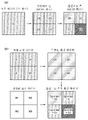
도 3은 업컨버트를 설명하는 도면이다.
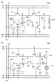
도 4는 화소 회로를 설명하는 도면이다.
도 5는 화소 회로의 동작을 설명하는 타이밍 차트이다.
도 6은 표시 장치를 설명하는 블록도이다.
도 7은 화소 회로를 설명하는 도면이다.
도 8은 표시 장치를 설명하는 블록도이다.
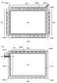
도 9는 표시 장치를 설명하는 도면이다.
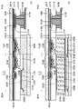
도 10은 표시 장치를 설명하는 도면이다.
도 11은 표시 장치의 동작 모드의 일례를 설명하는 도면이다.
도 12는 뉴럴 네트워크의 구성예를 설명하는 도면이다.
도 13은 반도체 장치의 구성예를 설명하는 도면이다.
도 14는 메모리 셀의 구성예를 설명하는 도면이다.
도 15는 오프셋 회로의 구성예를 설명하는 도면이다.
도 16은 반도체 장치의 동작을 설명하는 타이밍 차트이다.
도 17은 전자 기기를 설명하는 도면이다.
Claims (3)
- 표시 장치로서,
제 1 트랜지스터와, 제 2 트랜지스터와, 제 3 트랜지스터와, 제 1 용량 소자와, 제 2 용량 소자와, 표시 소자를 포함하는 화소를 가지고,
상기 제 1 트랜지스터의 소스 및 드레인 중 한쪽은 상기 제 1 용량 소자의 한쪽의 전극과 상기 표시 소자에 전기적으로 접속되고,
상기 제 2 트랜지스터의 소스 및 드레인 중 한쪽은 상기 제 1 용량 소자의 다른 쪽의 전극과 전기적으로 접속되고,
상기 제 2 트랜지스터의 게이트와, 상기 제 3 트랜지스터의 소스 및 드레인 중 한쪽은 상기 제 2 용량 소자의 한쪽의 전극과 전기적으로 접속되는, 표시 장치. - 제 1 항에 있어서,
상기 제1 트랜지스터, 상기 제 2 트랜지스터 및 상기 제 3 트랜지스터 중 적어도 하나는 채널 형성 영역에 금속 산화물을 가지고,
상기 금속 산화물은 In을 갖는, 표시 장치. - 제 1 항에 있어서,
상기 표시 소자는 액정 소자 또는 EL 소자인, 표시 장치.
Applications Claiming Priority (4)
| Application Number | Priority Date | Filing Date | Title |
|---|---|---|---|
| JP2017156237 | 2017-08-11 | ||
| JPJP-P-2017-156237 | 2017-08-11 | ||
| PCT/IB2018/055582 WO2019030595A1 (ja) | 2017-08-11 | 2018-07-26 | 表示装置および電子機器 |
| KR1020207001881A KR102472837B1 (ko) | 2017-08-11 | 2018-07-26 | 표시 장치 및 전자 기기 |
Related Parent Applications (1)
| Application Number | Title | Priority Date | Filing Date |
|---|---|---|---|
| KR1020207001881A Division KR102472837B1 (ko) | 2017-08-11 | 2018-07-26 | 표시 장치 및 전자 기기 |
Publications (1)
| Publication Number | Publication Date |
|---|---|
| KR20220165800A true KR20220165800A (ko) | 2022-12-15 |
Family
ID=65271021
Family Applications (2)
| Application Number | Title | Priority Date | Filing Date |
|---|---|---|---|
| KR1020207001881A Active KR102472837B1 (ko) | 2017-08-11 | 2018-07-26 | 표시 장치 및 전자 기기 |
| KR1020227041553A Ceased KR20220165800A (ko) | 2017-08-11 | 2018-07-26 | 표시 장치 및 전자 기기 |
Family Applications Before (1)
| Application Number | Title | Priority Date | Filing Date |
|---|---|---|---|
| KR1020207001881A Active KR102472837B1 (ko) | 2017-08-11 | 2018-07-26 | 표시 장치 및 전자 기기 |
Country Status (4)
| Country | Link |
|---|---|
| US (2) | US11054710B2 (ko) |
| JP (3) | JP7092767B2 (ko) |
| KR (2) | KR102472837B1 (ko) |
| WO (1) | WO2019030595A1 (ko) |
Families Citing this family (21)
| Publication number | Priority date | Publication date | Assignee | Title |
|---|---|---|---|---|
| KR102472837B1 (ko) * | 2017-08-11 | 2022-11-30 | 가부시키가이샤 한도오따이 에네루기 켄큐쇼 | 표시 장치 및 전자 기기 |
| WO2019043483A1 (en) | 2017-08-31 | 2019-03-07 | Semiconductor Energy Laboratory Co., Ltd. | DISPLAY DEVICE AND ELECTRONIC DEVICE |
| US11574573B2 (en) | 2017-09-05 | 2023-02-07 | Semiconductor Energy Laboratory Co., Ltd. | Display system |
| US11302278B2 (en) | 2017-09-15 | 2022-04-12 | Semiconductor Energy Laboratory Co., Ltd. | Display device including pixel and electronic device |
| KR20250159074A (ko) | 2017-11-02 | 2025-11-07 | 가부시키가이샤 한도오따이 에네루기 켄큐쇼 | 표시 장치 및 전자 기기 |
| CN111448608B (zh) | 2017-12-22 | 2025-07-08 | 株式会社半导体能源研究所 | 显示装置及电子设备 |
| JP7242558B2 (ja) | 2018-01-05 | 2023-03-20 | 株式会社半導体エネルギー研究所 | 表示モジュール |
| WO2019162801A1 (ja) | 2018-02-23 | 2019-08-29 | 株式会社半導体エネルギー研究所 | 表示装置の動作方法 |
| WO2019207404A1 (ja) | 2018-04-26 | 2019-10-31 | 株式会社半導体エネルギー研究所 | 半導体装置 |
| KR20210009326A (ko) | 2018-05-17 | 2021-01-26 | 가부시키가이샤 한도오따이 에네루기 켄큐쇼 | 표시 장치 |
| KR102849703B1 (ko) | 2018-05-25 | 2025-08-26 | 가부시키가이샤 한도오따이 에네루기 켄큐쇼 | 표시 장치 및 전자 기기 |
| CN119403406A (zh) | 2018-06-06 | 2025-02-07 | 株式会社半导体能源研究所 | 显示装置、显示模块及电子设备 |
| US10770482B2 (en) | 2018-06-06 | 2020-09-08 | Semiconductor Energy Laboratory Co., Ltd. | Display device and electronic device |
| WO2020016704A1 (ja) | 2018-07-20 | 2020-01-23 | 株式会社半導体エネルギー研究所 | 撮像パネル、撮像装置 |
| JP7315572B2 (ja) * | 2018-09-21 | 2023-07-26 | 株式会社半導体エネルギー研究所 | 表示装置および電子機器 |
| US11575013B2 (en) | 2018-11-02 | 2023-02-07 | Semiconductor Energy Laboratory Co., Ltd. | Semiconductor device and electronic device |
| JP7412360B2 (ja) | 2019-02-05 | 2024-01-12 | 株式会社半導体エネルギー研究所 | 表示装置および電子機器 |
| CN113841253A (zh) * | 2019-05-30 | 2021-12-24 | 株式会社半导体能源研究所 | 显示装置及电子设备 |
| TWI895279B (zh) | 2019-08-29 | 2025-09-01 | 日商半導體能源研究所股份有限公司 | 顯示裝置 |
| JP7517869B2 (ja) * | 2020-06-09 | 2024-07-17 | 武漢天馬微電子有限公司 | 表示装置 |
| US12300174B2 (en) | 2021-08-12 | 2025-05-13 | Semiconductor Energy Laboratory Co., Ltd. | Correction method of display apparatus including pixel and plurality of circuits |
Citations (3)
| Publication number | Priority date | Publication date | Assignee | Title |
|---|---|---|---|---|
| JP2007096055A (ja) | 2005-09-29 | 2007-04-12 | Semiconductor Energy Lab Co Ltd | 半導体装置、及び半導体装置の作製方法 |
| JP2007123861A (ja) | 2005-09-29 | 2007-05-17 | Semiconductor Energy Lab Co Ltd | 半導体装置及びその作製方法 |
| JP2011119674A (ja) | 2009-10-30 | 2011-06-16 | Semiconductor Energy Lab Co Ltd | 半導体装置 |
Family Cites Families (18)
| Publication number | Priority date | Publication date | Assignee | Title |
|---|---|---|---|---|
| JPH1184419A (ja) | 1997-09-09 | 1999-03-26 | Hitachi Ltd | 液晶ライトバルブおよび投射型表示装置 |
| JP3704984B2 (ja) | 1998-12-28 | 2005-10-12 | 株式会社日立製作所 | 液晶表示装置 |
| KR101043673B1 (ko) * | 2004-03-31 | 2011-06-22 | 엘지디스플레이 주식회사 | 스토리지 인버젼을 위한 스토리지 드라이버 |
| EP1998373A3 (en) | 2005-09-29 | 2012-10-31 | Semiconductor Energy Laboratory Co, Ltd. | Semiconductor device having oxide semiconductor layer and manufacturing method thereof |
| US8421716B2 (en) | 2006-08-30 | 2013-04-16 | Sharp Kabushiki Kaisha | Display device |
| JP5046226B2 (ja) * | 2007-04-02 | 2012-10-10 | 株式会社ジャパンディスプレイウェスト | 画像表示装置 |
| JP5131092B2 (ja) * | 2008-08-28 | 2013-01-30 | セイコーエプソン株式会社 | 電気光学装置および電子機器 |
| KR101771954B1 (ko) | 2010-06-22 | 2017-08-30 | 엘지디스플레이 주식회사 | 액정 표시장치 및 구동방법 |
| JP2013076812A (ja) | 2011-09-30 | 2013-04-25 | Sony Corp | 画素回路、画素回路の駆動方法、表示装置、および、電子機器 |
| JP6521794B2 (ja) | 2014-09-03 | 2019-05-29 | 株式会社半導体エネルギー研究所 | 半導体装置、及び電子機器 |
| US10140940B2 (en) | 2015-07-24 | 2018-11-27 | Japan Display Inc. | Display device |
| JP2017027012A (ja) | 2015-07-24 | 2017-02-02 | 株式会社ジャパンディスプレイ | 表示装置 |
| JP6853662B2 (ja) * | 2016-12-22 | 2021-03-31 | 株式会社Joled | 表示パネルおよび表示装置 |
| KR102472837B1 (ko) * | 2017-08-11 | 2022-11-30 | 가부시키가이샤 한도오따이 에네루기 켄큐쇼 | 표시 장치 및 전자 기기 |
| JP2019045614A (ja) | 2017-08-31 | 2019-03-22 | 株式会社半導体エネルギー研究所 | 表示装置および電子機器 |
| WO2019043483A1 (en) | 2017-08-31 | 2019-03-07 | Semiconductor Energy Laboratory Co., Ltd. | DISPLAY DEVICE AND ELECTRONIC DEVICE |
| JP2019045613A (ja) | 2017-08-31 | 2019-03-22 | 株式会社半導体エネルギー研究所 | 表示装置および電子機器 |
| US11574573B2 (en) * | 2017-09-05 | 2023-02-07 | Semiconductor Energy Laboratory Co., Ltd. | Display system |
-
2018
- 2018-07-26 KR KR1020207001881A patent/KR102472837B1/ko active Active
- 2018-07-26 WO PCT/IB2018/055582 patent/WO2019030595A1/ja not_active Ceased
- 2018-07-26 KR KR1020227041553A patent/KR20220165800A/ko not_active Ceased
- 2018-07-26 US US16/631,511 patent/US11054710B2/en active Active
- 2018-07-26 JP JP2019535999A patent/JP7092767B2/ja active Active
-
2021
- 2021-06-30 US US17/363,552 patent/US11681192B2/en active Active
-
2022
- 2022-06-16 JP JP2022097289A patent/JP7232371B2/ja active Active
-
2023
- 2023-02-17 JP JP2023023044A patent/JP2023063320A/ja not_active Withdrawn
Patent Citations (3)
| Publication number | Priority date | Publication date | Assignee | Title |
|---|---|---|---|---|
| JP2007096055A (ja) | 2005-09-29 | 2007-04-12 | Semiconductor Energy Lab Co Ltd | 半導体装置、及び半導体装置の作製方法 |
| JP2007123861A (ja) | 2005-09-29 | 2007-05-17 | Semiconductor Energy Lab Co Ltd | 半導体装置及びその作製方法 |
| JP2011119674A (ja) | 2009-10-30 | 2011-06-16 | Semiconductor Energy Lab Co Ltd | 半導体装置 |
Also Published As
| Publication number | Publication date |
|---|---|
| WO2019030595A1 (ja) | 2019-02-14 |
| US11054710B2 (en) | 2021-07-06 |
| US20210341777A1 (en) | 2021-11-04 |
| JP7092767B2 (ja) | 2022-06-28 |
| US11681192B2 (en) | 2023-06-20 |
| US20200142229A1 (en) | 2020-05-07 |
| JP2022137056A (ja) | 2022-09-21 |
| JP7232371B2 (ja) | 2023-03-02 |
| KR102472837B1 (ko) | 2022-11-30 |
| KR20200035945A (ko) | 2020-04-06 |
| JP2023063320A (ja) | 2023-05-09 |
| JPWO2019030595A1 (ja) | 2020-09-24 |
Similar Documents
| Publication | Publication Date | Title |
|---|---|---|
| KR102472837B1 (ko) | 표시 장치 및 전자 기기 | |
| KR102765869B1 (ko) | 표시 장치 및 전자 기기 | |
| US12446309B2 (en) | Display device and electronic device | |
| KR102642601B1 (ko) | 표시 장치 및 전자 기기 | |
| US11392005B2 (en) | Display device and electronic device | |
| JP2019045614A (ja) | 表示装置および電子機器 |
Legal Events
| Date | Code | Title | Description |
|---|---|---|---|
| A107 | Divisional application of patent | ||
| PA0104 | Divisional application for international application |
Comment text: Divisional Application for International Patent Patent event code: PA01041R01D Patent event date: 20221125 Application number text: 1020207001881 Filing date: 20200120 |
|
| PA0201 | Request for examination | ||
| PG1501 | Laying open of application | ||
| E902 | Notification of reason for refusal | ||
| PE0902 | Notice of grounds for rejection |
Comment text: Notification of reason for refusal Patent event date: 20221230 Patent event code: PE09021S01D |
|
| E90F | Notification of reason for final refusal | ||
| PE0902 | Notice of grounds for rejection |
Comment text: Final Notice of Reason for Refusal Patent event date: 20231230 Patent event code: PE09021S02D |
|
| E601 | Decision to refuse application | ||
| PE0601 | Decision on rejection of patent |
Patent event date: 20240312 Comment text: Decision to Refuse Application Patent event code: PE06012S01D Patent event date: 20231230 Comment text: Final Notice of Reason for Refusal Patent event code: PE06011S02I Patent event date: 20221230 Comment text: Notification of reason for refusal Patent event code: PE06011S01I |