KR20250071663A - Multilayer electronic component - Google Patents
Multilayer electronic component Download PDFInfo
- Publication number
- KR20250071663A KR20250071663A KR1020230158445A KR20230158445A KR20250071663A KR 20250071663 A KR20250071663 A KR 20250071663A KR 1020230158445 A KR1020230158445 A KR 1020230158445A KR 20230158445 A KR20230158445 A KR 20230158445A KR 20250071663 A KR20250071663 A KR 20250071663A
- Authority
- KR
- South Korea
- Prior art keywords
- gallium
- side margin
- dielectric layer
- electronic components
- cover portion
- Prior art date
- Legal status (The legal status is an assumption and is not a legal conclusion. Google has not performed a legal analysis and makes no representation as to the accuracy of the status listed.)
- Pending
Links
Images



Classifications
-
- H—ELECTRICITY
- H01—ELECTRIC ELEMENTS
- H01G—CAPACITORS; CAPACITORS, RECTIFIERS, DETECTORS, SWITCHING DEVICES, LIGHT-SENSITIVE OR TEMPERATURE-SENSITIVE DEVICES OF THE ELECTROLYTIC TYPE
- H01G4/00—Fixed capacitors; Processes of their manufacture
- H01G4/002—Details
- H01G4/224—Housing; Encapsulation
-
- H—ELECTRICITY
- H01—ELECTRIC ELEMENTS
- H01G—CAPACITORS; CAPACITORS, RECTIFIERS, DETECTORS, SWITCHING DEVICES, LIGHT-SENSITIVE OR TEMPERATURE-SENSITIVE DEVICES OF THE ELECTROLYTIC TYPE
- H01G4/00—Fixed capacitors; Processes of their manufacture
- H01G4/30—Stacked capacitors
-
- H—ELECTRICITY
- H01—ELECTRIC ELEMENTS
- H01G—CAPACITORS; CAPACITORS, RECTIFIERS, DETECTORS, SWITCHING DEVICES, LIGHT-SENSITIVE OR TEMPERATURE-SENSITIVE DEVICES OF THE ELECTROLYTIC TYPE
- H01G2/00—Details of capacitors not covered by a single one of groups H01G4/00-H01G11/00
- H01G2/12—Protection against corrosion
-
- H—ELECTRICITY
- H01—ELECTRIC ELEMENTS
- H01G—CAPACITORS; CAPACITORS, RECTIFIERS, DETECTORS, SWITCHING DEVICES, LIGHT-SENSITIVE OR TEMPERATURE-SENSITIVE DEVICES OF THE ELECTROLYTIC TYPE
- H01G4/00—Fixed capacitors; Processes of their manufacture
- H01G4/002—Details
- H01G4/005—Electrodes
- H01G4/008—Selection of materials
-
- H—ELECTRICITY
- H01—ELECTRIC ELEMENTS
- H01G—CAPACITORS; CAPACITORS, RECTIFIERS, DETECTORS, SWITCHING DEVICES, LIGHT-SENSITIVE OR TEMPERATURE-SENSITIVE DEVICES OF THE ELECTROLYTIC TYPE
- H01G4/00—Fixed capacitors; Processes of their manufacture
- H01G4/002—Details
- H01G4/005—Electrodes
- H01G4/012—Form of non-self-supporting electrodes
-
- H—ELECTRICITY
- H01—ELECTRIC ELEMENTS
- H01G—CAPACITORS; CAPACITORS, RECTIFIERS, DETECTORS, SWITCHING DEVICES, LIGHT-SENSITIVE OR TEMPERATURE-SENSITIVE DEVICES OF THE ELECTROLYTIC TYPE
- H01G4/00—Fixed capacitors; Processes of their manufacture
- H01G4/002—Details
- H01G4/018—Dielectrics
- H01G4/06—Solid dielectrics
- H01G4/08—Inorganic dielectrics
- H01G4/12—Ceramic dielectrics
-
- H—ELECTRICITY
- H01—ELECTRIC ELEMENTS
- H01G—CAPACITORS; CAPACITORS, RECTIFIERS, DETECTORS, SWITCHING DEVICES, LIGHT-SENSITIVE OR TEMPERATURE-SENSITIVE DEVICES OF THE ELECTROLYTIC TYPE
- H01G4/00—Fixed capacitors; Processes of their manufacture
- H01G4/002—Details
- H01G4/018—Dielectrics
- H01G4/06—Solid dielectrics
- H01G4/08—Inorganic dielectrics
- H01G4/12—Ceramic dielectrics
- H01G4/1209—Ceramic dielectrics characterised by the ceramic dielectric material
-
- H—ELECTRICITY
- H01—ELECTRIC ELEMENTS
- H01G—CAPACITORS; CAPACITORS, RECTIFIERS, DETECTORS, SWITCHING DEVICES, LIGHT-SENSITIVE OR TEMPERATURE-SENSITIVE DEVICES OF THE ELECTROLYTIC TYPE
- H01G4/00—Fixed capacitors; Processes of their manufacture
- H01G4/002—Details
- H01G4/018—Dielectrics
- H01G4/06—Solid dielectrics
- H01G4/08—Inorganic dielectrics
- H01G4/12—Ceramic dielectrics
- H01G4/1209—Ceramic dielectrics characterised by the ceramic dielectric material
- H01G4/1218—Ceramic dielectrics characterised by the ceramic dielectric material based on titanium oxides or titanates
- H01G4/1227—Ceramic dielectrics characterised by the ceramic dielectric material based on titanium oxides or titanates based on alkaline earth titanates
-
- H—ELECTRICITY
- H01—ELECTRIC ELEMENTS
- H01G—CAPACITORS; CAPACITORS, RECTIFIERS, DETECTORS, SWITCHING DEVICES, LIGHT-SENSITIVE OR TEMPERATURE-SENSITIVE DEVICES OF THE ELECTROLYTIC TYPE
- H01G4/00—Fixed capacitors; Processes of their manufacture
- H01G4/002—Details
- H01G4/018—Dielectrics
- H01G4/06—Solid dielectrics
- H01G4/08—Inorganic dielectrics
- H01G4/12—Ceramic dielectrics
- H01G4/1272—Semiconductive ceramic capacitors
- H01G4/1281—Semiconductive ceramic capacitors with grain boundary layer
-
- H—ELECTRICITY
- H01—ELECTRIC ELEMENTS
- H01G—CAPACITORS; CAPACITORS, RECTIFIERS, DETECTORS, SWITCHING DEVICES, LIGHT-SENSITIVE OR TEMPERATURE-SENSITIVE DEVICES OF THE ELECTROLYTIC TYPE
- H01G4/00—Fixed capacitors; Processes of their manufacture
- H01G4/002—Details
- H01G4/228—Terminals
- H01G4/232—Terminals electrically connecting two or more layers of a stacked or rolled capacitor
-
- Y—GENERAL TAGGING OF NEW TECHNOLOGICAL DEVELOPMENTS; GENERAL TAGGING OF CROSS-SECTIONAL TECHNOLOGIES SPANNING OVER SEVERAL SECTIONS OF THE IPC; TECHNICAL SUBJECTS COVERED BY FORMER USPC CROSS-REFERENCE ART COLLECTIONS [XRACs] AND DIGESTS
- Y02—TECHNOLOGIES OR APPLICATIONS FOR MITIGATION OR ADAPTATION AGAINST CLIMATE CHANGE
- Y02E—REDUCTION OF GREENHOUSE GAS [GHG] EMISSIONS, RELATED TO ENERGY GENERATION, TRANSMISSION OR DISTRIBUTION
- Y02E60/00—Enabling technologies; Technologies with a potential or indirect contribution to GHG emissions mitigation
- Y02E60/13—Energy storage using capacitors
Landscapes
- Engineering & Computer Science (AREA)
- Power Engineering (AREA)
- Microelectronics & Electronic Packaging (AREA)
- Manufacturing & Machinery (AREA)
- Chemical & Material Sciences (AREA)
- Ceramic Engineering (AREA)
- Inorganic Chemistry (AREA)
- Materials Engineering (AREA)
- Fixed Capacitors And Capacitor Manufacturing Machines (AREA)
- Ceramic Capacitors (AREA)
- Coils Or Transformers For Communication (AREA)
Abstract
본 발명의 일 실시형태에 따른 적층형 전자 부품은, 유전체층 및 내부 전극을 포함하는 바디; 상기 바디 상에 배치되는 외부 전극; 및 상기 바디 상에 배치되는 사이드 마진부; 를 포함하고, 상기 커버부 및 사이드 마진부는 티타늄(Ti) 및 갈륨(Ga)을 포함하며, 상기 커버부에 포함된 티타늄(Ti) 100 몰 대비 갈륨(Ga)의 몰 수(A)에 대한, 상기 사이드 마진부에 포함된 티타늄(Ti) 100 몰 대비 갈륨(Ga)의 몰 수(B)의 비율(B/A)은 1.5 ≤ B/A 를 만족할 수 있다.According to one embodiment of the present invention, a laminated electronic component comprises: a body including a dielectric layer and an internal electrode; an external electrode disposed on the body; and a side margin portion disposed on the body; wherein the cover portion and the side margin portion include titanium (Ti) and gallium (Ga), and a ratio (B/A) of the number of moles of gallium (Ga) per 100 moles of titanium (Ti) included in the cover portion to the number of moles of gallium (Ga) per 100 moles of titanium (Ti) included in the side margin portion can satisfy 1.5 ≤ B/A.
Description
본 발명은 적층형 전자 부품에 관한 것이다.The present invention relates to a laminated electronic component.
적층형 전자 부품의 하나인 적층 세라믹 커패시터(MLCC: Multi-Layered Ceramic Capacitor)는 액정 표시 장치(LCD: Liquid Crystal Display) 및 플라즈마 표시 장치 패널(PDP: Plasma Display Panel) 등의 영상 기기, 컴퓨터, 스마트폰 및 휴대폰 등 여러 전자 제품의 인쇄회로기판에 장착되어 전기를 충전시키거나 또는 방전시키는 역할을 하는 칩 형태의 콘덴서이다.Multilayer ceramic capacitor (MLCC), a type of multilayer electronic component, is a chip-shaped capacitor that is mounted on the printed circuit boards of various electronic products such as video devices such as liquid crystal displays (LCDs) and plasma display panels (PDPs), computers, smartphones, and mobile phones to charge or discharge electricity.
이러한 적층 세라믹 커패시터는 소형이면서 고용량이 보장되고 실장이 용이하다는 장점으로 인하여 다양한 전자 장치의 부품으로 사용될 수 있다. 컴퓨터, 모바일 기기 등 각종 전자 기기가 소형화, 고출력화되면서 적층 세라믹 커패시터에 대한 소형화 및 고용량화의 요구가 증대되고 있다. These multilayer ceramic capacitors can be used as components of various electronic devices because they are small in size, have high capacity, and are easy to install. As various electronic devices such as computers and mobile devices become smaller and have higher output, the demand for multilayer ceramic capacitors is increasing in size and capacity.
소형화 및 고용량화가 진행됨에 따라 용량을 형성하는 영역을 보호할 필요성이 높아지고 있는데, 이는 용량을 형성하는 영역을 둘러싸는 마진영역을 추가하여 이를 개선하고 있다. 다만, 소형화 및 고용량화를 달성하기 위해 구조적인 설계를 지속적으로 변경함에 따라, 용량을 형성하는 영역은 커지고 용량을 형성하는 영역을 보호하는 마진영역이 줄어들면서, 적층 세라믹 커패시터의 내습 신뢰성 및 강도가 취약해지는 문제점이 발생할 우려가 있다. As miniaturization and high-capacity progress, the need to protect the area forming the capacity is increasing, and this is being improved by adding a margin area surrounding the area forming the capacity. However, as the structural design is continuously changed to achieve miniaturization and high-capacity, the area forming the capacity is increasing and the margin area protecting the area forming the capacity is decreasing, so there is a concern that the moisture-resistant reliability and strength of the multilayer ceramic capacitor will become weak.
본 발명이 해결하고자 하는 여러 과제 중 하나는 내습 신뢰성이 향상된 적층형 전자 부품을 제공하기 위함이다.One of the many problems that the present invention seeks to solve is to provide a laminated electronic component with improved moisture resistance reliability.
본 발명이 해결하고자 하는 여러 과제 중 하나는 기계적 특성이 향상된 적층형 전자 부품을 제공하기 위함이다.One of the many problems that the present invention seeks to solve is to provide a laminated electronic component with improved mechanical properties.
다만, 본 발명이 해결하고자 하는 여러 과제는 상술한 내용에 한정되지 않으며, 본 발명의 구체적인 실시형태를 설명하는 과정에서 보다 쉽게 이해될 수 있을 것이다.However, the various problems to be solved by the present invention are not limited to the above-described contents, and will be more easily understood in the process of explaining specific embodiments of the present invention.
본 발명의 일 실시형태에 따른 적층형 전자 부품은, 유전체층 및 상기 유전체층과 제1 방향으로 번갈아 배치되는 내부 전극을 포함하는 용량 형성부, 및 상기 용량 형성부의 상기 제1 방향 양 단면(end-surface)에 배치되는 커버부를 포함하고, 상기 제1 방향으로 서로 마주보는 제1 및 제2 면, 상기 제1 및 제2 면과 연결되고 제2 방향으로 서로 마주보는 제3 및 제4 면, 상기 제1 내지 제4 면과 연결되고 제3 방향으로 서로 마주보는 제5 및 제6 면을 포함하는 바디; 상기 제3 및 제4 면에 배치되는 외부 전극; 및 상기 제5 및 제6 면에 배치되는 사이드 마진부; 를 포함하고, 상기 커버부 및 사이드 마진부는 티타늄(Ti) 및 갈륨(Ga)을 포함하며, 상기 커버부에 포함된 티타늄(Ti) 100 몰 대비 갈륨(Ga)의 몰 수(A)에 대한, 상기 사이드 마진부에 포함된 티타늄(Ti) 100 몰 대비 갈륨(Ga)의 몰 수(B)의 비율(B/A)은 1.5 ≤ B/A 를 만족할 수 있다.According to one embodiment of the present invention, a laminated electronic component comprises: a capacitance forming portion including a dielectric layer and internal electrodes alternately arranged with the dielectric layer in a first direction; and a cover portion arranged on both end-surfaces of the capacitance forming portion in the first direction, the body including first and second surfaces facing each other in the first direction, third and fourth surfaces connected to the first and second surfaces and facing each other in the second direction, and fifth and sixth surfaces connected to the first to fourth surfaces and facing each other in the third direction; external electrodes arranged on the third and fourth surfaces; and side margin portions arranged on the fifth and sixth surfaces. , and the cover portion and the side margin portion include titanium (Ti) and gallium (Ga), and a ratio (B/A) of the number of moles of gallium (Ga) per 100 moles of titanium (Ti) included in the cover portion to the number of moles of gallium (Ga) per 100 moles of titanium (Ti) included in the side margin portion can satisfy 1.5 ≤ B/A.
본 발명의 여러 효과 중 하나는 적층형 전자 부품의 내습 신뢰성이 향상된 것이다.One of the many effects of the present invention is improved moisture resistance reliability of laminated electronic components.
본 발명의 여러 효과 중 하나는 적층형 전자 부품의 기계적 특성이 향상된 것이다.One of the many effects of the present invention is that the mechanical properties of laminated electronic components are improved.
다만, 본 발명의 다양하면서도 유익한 장점과 효과는 상술한 내용에 한정되지 않으며, 본 발명의 구체적인 실시형태를 설명하는 과정에서 보다 쉽게 이해될 수 있을 것이다.However, the various advantageous and beneficial advantages and effects of the present invention are not limited to the above-described contents, and will be more easily understood in the process of explaining specific embodiments of the present invention.
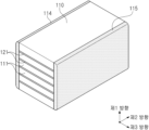
도 1은 본 발명의 일 실시형태에 따른 적층형 전자 부품의 사시도를 개략적으로 도시한 것이다.
도 2는 도 1의 적층형 전자 부품에서 외부 전극을 제외한 사시도를 개략적으로 도시한 것이다.
도 3은 도 1의 적층형 전자 부품에서 외부 전극 및 사이드 마진부를 제외한 사시도를 개략적으로 도시한 것이다.
도 4는 내부 전극의 적층 구조를 나타낸 분리사시도를 개략적으로 도시한 것이다.
도 5는 도 1의 I-I'에 따른 단면도를 개략적으로 도시한 것이다.
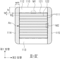
도 6은 도 1의 II-II'에 따른 단면도를 개략적으로 도시한 것이다.
도 7a 및 도 7b는 비교예에 있어서 도 6의 M1 및 M2 영역을 주사전자현미경(SEM)으로 촬영한 이미지이고, 도 7c 및 도 7d는 실시예에 있어서 도 6의 M1 및 M2 영역을 주사전자현미경(SEM)으로 촬영한 이미지이다.
도 8a는 비교예의 커버부 단면을 주사전자현미경(SEM)의 HAADF 모드로 촬영한 이미지이며, 도 8b는 도 8a의 영역에서 EDS 분석을 진행하여 알루미늄(Al) 원소를 맵핑(mapping)한 이미지이고, 도 8c는 도 8a의 영역에서 EDS 분석을 진행하여 규소(Si) 원소를 맵핑(mapping)한 이미지이다.
도 9a는 실시예의 커버부 단면을 주사전자현미경(SEM)의 HAADF 모드로 촬영한 이미지이며, 도 9b는 도 9a의 영역에서 EDS 분석을 진행하여 알루미늄(Al) 원소를 맵핑(mapping)한 이미지이고, 도 9c는 도 9a의 영역에서 EDS 분석을 진행하여 규소(Si) 원소를 맵핑(mapping)한 이미지이며, 도 9d는 도 9a의 영역에서 EDS 분석을 진행하여 갈륨(Ga) 원소를 맵핑(mapping)한 이미지이다.
도 10a는 비교예의 사이드 마진부 단면을 주사전자현미경(SEM)의 HAADF 모드로 촬영한 이미지이며, 도 10b는 도 10a의 영역에서 EDS 분석을 진행하여 알루미늄(Al) 원소를 맵핑(mapping)한 이미지이고, 도 10c는 도 10a의 영역에서 EDS 분석을 진행하여 규소(Si) 원소를 맵핑(mapping)한 이미지이다.
도 11a는 실시예의 사이드 마진부 단면을 주사전자현미경(SEM)의 HAADF 모드로 촬영한 이미지이며, 도 11b는 도 11a의 영역에서 EDS 분석을 진행하여 알루미늄(Al) 원소를 맵핑(mapping)한 이미지이고, 도 11c는 도 11a의 영역에서 EDS 분석을 진행하여 규소(Si) 원소를 맵핑(mapping)한 이미지이며, 도 11d는 도 11a의 영역에서 EDS 분석을 진행하여 갈륨(Ga) 원소를 맵핑(mapping)한 이미지이다.
도 12a 및 도 12b는 비교예의 내습 신뢰성 평가 그래프이고, 도 12c 및 도 12d는 실시예의 내습 신뢰성 평가 그래프이다.
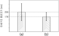
도 13a는 비교예의 결정립 미세구조 크기에 관한 그래프이고, 도 13b는 실시예의 결정립 미세구조 크기에 관한 그래프이다.FIG. 1 is a schematic perspective view of a laminated electronic component according to one embodiment of the present invention.
FIG. 2 is a schematic perspective view of the laminated electronic component of FIG. 1, excluding the external electrodes.
FIG. 3 is a schematic perspective view of the laminated electronic component of FIG. 1, excluding the external electrodes and side margins.
Figure 4 is a schematic diagram illustrating an exploded perspective view showing the laminated structure of the internal electrode.
Figure 5 is a schematic illustration of a cross-sectional view taken along line I-I' of Figure 1.
Figure 6 schematically illustrates a cross-sectional view along II-II' of Figure 1.
FIGS. 7a and 7b are images of the M1 and M2 regions of FIG. 6 taken with a scanning electron microscope (SEM) in a comparative example, and FIGS. 7c and 7d are images of the M1 and M2 regions of FIG. 6 taken with a scanning electron microscope (SEM) in an example.
Fig. 8a is an image of a cross-section of a cover portion of a comparative example taken in HAADF mode of a scanning electron microscope (SEM), Fig. 8b is an image of aluminum (Al) elements mapped by performing EDS analysis in the area of Fig. 8a, and Fig. 8c is an image of silicon (Si) elements mapped by performing EDS analysis in the area of Fig. 8a.
FIG. 9a is an image of a cross-section of a cover portion of an embodiment taken in HAADF mode of a scanning electron microscope (SEM), FIG. 9b is an image of aluminum (Al) element mapping by performing EDS analysis in the area of FIG. 9a, FIG. 9c is an image of silicon (Si) element mapping by performing EDS analysis in the area of FIG. 9a, and FIG. 9d is an image of gallium (Ga) element mapping by performing EDS analysis in the area of FIG. 9a.
Fig. 10a is an image of a cross-section of a side margin portion of a comparative example taken in HAADF mode of a scanning electron microscope (SEM), Fig. 10b is an image of aluminum (Al) elements mapped by performing EDS analysis in the area of Fig. 10a, and Fig. 10c is an image of silicon (Si) elements mapped by performing EDS analysis in the area of Fig. 10a.
Fig. 11a is an image of a cross-section of a side margin portion of an example taken in HAADF mode of a scanning electron microscope (SEM), Fig. 11b is an image of mapping aluminum (Al) elements by performing EDS analysis in the area of Fig. 11a, Fig. 11c is an image of mapping silicon (Si) elements by performing EDS analysis in the area of Fig. 11a, and Fig. 11d is an image of mapping gallium (Ga) elements by performing EDS analysis in the area of Fig. 11a.
Figures 12a and 12b are moisture resistance reliability evaluation graphs of a comparative example, and Figures 12c and 12d are moisture resistance reliability evaluation graphs of an embodiment.
Fig. 13a is a graph regarding the crystal grain microstructure size of a comparative example, and Fig. 13b is a graph regarding the crystal grain microstructure size of an example.
이하, 구체적인 실시형태 및 첨부된 도면을 참조하여 본 발명의 실시형태를 설명한다. 그러나, 본 발명의 실시형태는 여러 가지 다른 형태로 변형될 수 있으며, 본 발명의 범위가 이하 설명하는 실시형태로 한정되는 것은 아니다. 또한, 본 발명의 실시형태는 통상의 기술자에게 본 발명을 더욱 완전하게 설명하기 위해서 제공되는 것이다. 따라서, 도면에서의 요소들의 형상 및 크기 등은 보다 명확한 설명을 위해 과장될 수 있으며, 도면상의 동일한 부호로 표시되는 요소는 동일한 요소이다.Hereinafter, embodiments of the present invention will be described with reference to specific embodiments and the attached drawings. However, the embodiments of the present invention may be modified in various other forms, and the scope of the present invention is not limited to the embodiments described below. In addition, the embodiments of the present invention are provided to more completely explain the present invention to those skilled in the art. Therefore, the shapes and sizes of elements in the drawings may be exaggerated for clearer description, and elements indicated by the same symbols in the drawings are the same elements.
그리고 도면에서 본 발명을 명확하게 설명하기 위해서 설명과 관계없는 부분은 생략하고, 도면에서 나타난 각 구성의 크기 및 두께는 설명의 편의를 위해 임의로 나타내었으므로, 본 발명이 반드시 도시된 바에 한정되지 않는다. 또한, 동일한 사상의 범위 내의 기능이 동일한 구성요소는 동일한 참조부호를 사용하여 설명한다. 나아가, 명세서 전체에서, 어떤 부분이 어떤 구성요소를 "포함"한다고 할 때, 이는 특별히 반대되는 기재가 없는 한 다른 구성요소를 제외하는 것이 아니라 다른 구성요소를 더 포함할 수 있는 것을 의미한다.And in order to clearly explain the present invention in the drawings, parts that are not related to the explanation are omitted, and the size and thickness of each component shown in the drawings are arbitrarily shown for the convenience of explanation, so the present invention is not necessarily limited to what is shown. In addition, components with the same function within the scope of the same idea are described using the same reference numerals. Furthermore, throughout the specification, when a part is said to "include" a certain component, this does not mean that other components are excluded, but that other components can be further included, unless specifically stated otherwise.
도면에서, 제1 방향은 적층 방향 또는 두께(T) 방향, 제2 방향은 길이(L) 방향, 제3 방향은 폭(W) 방향으로 정의될 수 있다. In the drawing, the first direction can be defined as the stacking direction or thickness (T) direction, the second direction can be defined as the length (L) direction, and the third direction can be defined as the width (W) direction.
적층형Stacked 전자 부품Electronic components
도 1은 본 발명의 일 실시형태에 따른 적층형 전자 부품의 사시도를 개략적으로 도시한 것이다.FIG. 1 is a schematic perspective view of a laminated electronic component according to one embodiment of the present invention.
도 2는 도 1의 적층형 전자 부품에서 외부 전극을 제외한 사시도를 개략적으로 도시한 것이다.FIG. 2 is a schematic perspective view of the laminated electronic component of FIG. 1, excluding the external electrodes.
도 3은 도 1의 적층형 전자 부품에서 외부 전극 및 사이드 마진부를 제외한 사시도를 개략적으로 도시한 것이다.FIG. 3 is a schematic perspective view of the laminated electronic component of FIG. 1, excluding the external electrodes and side margins.
도 4는 내부 전극의 적층 구조를 나타낸 분리사시도를 개략적으로 도시한 것이다.Figure 4 is a schematic diagram illustrating an exploded perspective view showing the laminated structure of the internal electrode.
도 5는 도 1의 I-I'에 따른 단면도를 개략적으로 도시한 것이다.Figure 5 is a schematic illustration of a cross-sectional view taken along line I-I' of Figure 1.
도 6은 도 1의 II-II'에 따른 단면도를 개략적으로 도시한 것이다.Figure 6 schematically illustrates a cross-sectional view along II-II' of Figure 1.
이하, 도 1 내지 도 6을 참조하여, 본 발명의 일 실시형태에 따른 적층형 전자 부품에 대하여 상세히 설명한다. 다만, 적층형 전자 부품의 일례로서 적층 세라믹 커패시터에 대하여 설명하나, 본 발명은 유전체 조성물을 이용하는 다양한 전자 제품, 예를 들어, 인덕터, 압전체 소자, 바리스터, 또는 서미스터 등에도 적용될 수 있을 것이다. Hereinafter, with reference to FIGS. 1 to 6, a multilayer electronic component according to one embodiment of the present invention will be described in detail. However, a multilayer ceramic capacitor will be described as an example of the multilayer electronic component, but the present invention can also be applied to various electronic products that utilize a dielectric composition, such as an inductor, a piezoelectric element, a varistor, or a thermistor.
본 발명의 일 실시형태에 따른 적층형 전자 부품(100)은, 유전체층(111) 및 상기 유전체층(111)과 제1 방향으로 번갈아 배치되는 내부 전극(121, 122)을 포함하는 용량 형성부(Ac), 및 상기 용량 형성부(Ac)의 상기 제1 방향 양 단면(end-surface)에 배치되는 커버부(112, 113)를 포함하고, 상기 제1 방향으로 서로 마주보는 제1 및 제2 면(1, 2), 상기 제1 및 제2 면(1, 2)과 연결되고 제2 방향으로 서로 마주보는 제3 및 제4 면(3, 4), 상기 제1 내지 제4 면(1, 2, 3, 4)과 연결되고 제3 방향으로 서로 마주보는 제5 및 제6 면(5, 6)을 포함하는 바디(110); 상기 제3 및 제4 면(3, 4)에 배치되는 외부 전극; 및 상기 제5 및 제6 면(5, 6)에 배치되는 사이드 마진부(114, 115); 를 포함하고, 상기 커버부(112, 113) 및 사이드 마진부(114, 115)는 티타늄(Ti) 및 갈륨(Ga)을 포함하며, 상기 커버부(112, 113)에 포함된 티타늄(Ti) 100 몰 대비 갈륨(Ga)의 몰 수(A)에 대한, 사이드 마진부(114, 115)에 포함된 티타늄(Ti) 100 몰 대비 갈륨(Ga)의 몰 수(B)의 비율(B/A)은 1.5 ≤ B/A 를 만족할 수 있다.According to one embodiment of the present invention, a laminated electronic component (100) comprises a capacitance forming portion (Ac) including a dielectric layer (111) and internal electrodes (121, 122) alternately arranged with the dielectric layer (111) in a first direction, and cover portions (112, 113) arranged on both end surfaces of the capacitance forming portion (Ac) in the first direction, and comprises a body (110) including first and second surfaces (1, 2) facing each other in the first direction, third and fourth surfaces (3, 4) connected to the first and second surfaces (1, 2) and facing each other in the second direction, and fifth and sixth surfaces (5, 6) connected to the first to fourth surfaces (1, 2, 3, 4) and facing each other in the third direction; external electrodes arranged on the third and fourth surfaces (3, 4); And side margin portions (114, 115) arranged on the fifth and sixth surfaces (5, 6); and the cover portions (112, 113) and the side margin portions (114, 115) include titanium (Ti) and gallium (Ga), and a ratio (B/A) of the number of moles of gallium (Ga) per 100 moles of titanium (Ti) included in the cover portions (112, 113) to the number of moles of gallium (Ga) per 100 moles of titanium (Ti) included in the side margin portions (114, 115) can satisfy 1.5 ≤ B/A.
바디(110)는 유전체층(111) 및 내부 전극(121, 122)이 교대로 적층 되어있을 수 있다.The body (110) may have dielectric layers (111) and internal electrodes (121, 122) alternately laminated.
보다 구체적으로, 바디(110)는 바디(110)의 내부에 배치되며, 유전체층(111)을 사이에 두고 서로 마주보도록 번갈아 배치되는 제1 내부 전극(121) 및 제2 내부 전극(122)을 포함하여 용량을 형성하는 용량 형성부(Ac)를 포함할 수 있다. More specifically, the body (110) may include a capacitance forming portion (Ac) that forms a capacitance, including a first internal electrode (121) and a second internal electrode (122) that are arranged alternately to face each other with a dielectric layer (111) interposed therebetween, and are disposed inside the body (110).
바디(110)의 구체적인 형상에 특별히 제한은 없지만, 도시된 바와 같이 바디(110)는 육면체 형상이나 이와 유사한 형상으로 이루어질 수 있다. 소성 과정에서 바디(110)에 포함된 세라믹 입자의 수축으로 인하여, 바디(110)는 완전한 직선을 가진 육면체 형상은 아니지만 실질적으로 육면체 형상을 가질 수 있다.There is no particular limitation on the specific shape of the body (110), but as illustrated, the body (110) may be formed in a hexahedral shape or a similar shape. Due to shrinkage of the ceramic particles included in the body (110) during the firing process, the body (110) may not have a hexahedral shape with perfect straight lines, but may have a substantially hexahedral shape.
바디(110)는 제1 방향으로 서로 마주보는 제1 및 제2 면(1, 2), 제1 및 제2 면(1, 2)과 연결되고 제2 방향으로 서로 마주보는 제3 및 제4 면(3, 4), 제1 내지 제4 면(1, 2, 3, 4)과 연결되며 제3 방향으로 서로 마주보는 제5 및 제6 면(5, 6)을 가질 수 있다.The body (110) may have first and second faces (1, 2) facing each other in a first direction, third and fourth faces (3, 4) connected to the first and second faces (1, 2) and facing each other in a second direction, and fifth and sixth faces (5, 6) connected to the first to fourth faces (1, 2, 3, 4) and facing each other in a third direction.
바디(110)를 형성하는 복수의 유전체층(111)은 소성된 상태로서, 인접하는 유전체층(111) 사이의 경계는 주사전자현미경(Scanning Electron Microscope, SEM)을 이용하지 않고서는 확인하기 곤란할 정도로 일체화될 수 있다.A plurality of dielectric layers (111) forming a body (110) are in a sintered state, and the boundary between adjacent dielectric layers (111) can be integrated to such an extent that it is difficult to confirm without using a scanning electron microscope (SEM).
유전체층(111)을 형성하는 원료는 충분한 정전 용량을 얻을 수 있는 한 제한되지 않는다. 일반적으로 페로브스카이트(ABO3)계 재료를 사용할 수 있으며, 예를 들어, 티탄산바륨계 재료, 납 복합 페로브스카이트계 재료 또는 티탄산스트론튬계 재료 등을 사용할 수 있다. 티탄산바륨계 재료는 BaTiO3계 세라믹 입자를 포함할 수 있으며, 세라믹 입자의 예시로 BaTiO3, BaTiO3에 Ca(칼슘), Zr(지르코늄) 등이 일부 고용된 (Ba1 - xCax)TiO3 (0<x<1), Ba(Ti1-yCay)O3 (0<y<1), (Ba1 - xCax)(Ti1 - yZry)O3 (0<x<1, 0<y<1) 또는 Ba(Ti1-yZry)O3 (0<y<1) 등을 들 수 있다.The raw material forming the dielectric layer (111) is not limited as long as sufficient electrostatic capacity can be obtained. Generally, a perovskite (ABO 3 ) material can be used, and for example, a barium titanate material, a lead composite perovskite material, or a strontium titanate material can be used. The barium titanate-based material may include BaTiO 3 series ceramic particles. Examples of the ceramic particles include BaTiO 3 , BaTiO 3 partially dissolved with Ca (calcium), Zr (zirconium), etc. (Ba 1 - x Ca x )TiO 3 (0<x<1), Ba(Ti 1-y Ca y )O 3 (0<y<1), (Ba 1 - x Ca x )(Ti 1 - y Zr y )O 3 (0<x<1, 0<y<1), or Ba(Ti 1-y Zr y )O 3 (0<y<1).
또한, 유전체층(111)을 형성하는 원료는 티탄산바륨(BaTiO3) 등의 입자에 본 발명의 목적에 따라 다양한 세라믹 첨가제, 유기용제, 결합제, 분산제 등이 첨가될 수 있다.In addition, the raw material forming the dielectric layer (111) may be particles such as barium titanate (BaTiO 3 ), to which various ceramic additives, organic solvents, binders, dispersants, etc. may be added according to the purpose of the present invention.
또한, 유전체층(111)은 티탄산바륨(BaTiO3)과 같은 유전체 물질을 이용하여 형성될 수 있으므로, 소성 후 유전체 미세구조를 포함할 수 있다. 유전체 미세구조는, 복수의 결정립, 상기 인접한 결정립 사이에 배치되는 결정립계, 및 상기 결정립계가 3 개 이상 접하는 지점에 배치되는 삼중점을 포함할 수 있으며, 각각 복수 개를 포함할 수 있다.In addition, since the dielectric layer (111) can be formed using a dielectric material such as barium titanate (BaTiO 3 ), it can include a dielectric microstructure after firing. The dielectric microstructure can include a plurality of crystal grains, grain boundaries arranged between the adjacent crystal grains, and triple points arranged at points where three or more of the crystal grain boundaries come into contact, and each can include a plurality of them.
본 발명에서는, 후술하는 커버부(112, 113) 및 사이드 마진부(114, 115)에 포함되는 유전체층과 구분하기 위해, 용량 형성부(Ac)에 포함된 유전체층(111)은 제1 유전체층(111)이라고 정의할 수 있고, 커버부(112, 113)에 포함된 유전체층은 제2 유전체층이라고 정의할 수 있으며, 사이드 마진부(114, 115)에 포함되는 유전체층은 제3 유전체층이라고 정의할 수 있다.In the present invention, in order to distinguish it from the dielectric layers included in the cover portions (112, 113) and side margin portions (114, 115) described later, the dielectric layer (111) included in the capacitance forming portion (Ac) can be defined as a first dielectric layer (111), the dielectric layer included in the cover portions (112, 113) can be defined as a second dielectric layer, and the dielectric layer included in the side margin portions (114, 115) can be defined as a third dielectric layer.
본 발명의 일 실시형태에 있어서, 용량 형성부(Ac)의 유전체층(111)은 갈륨(Ga)을 포함하지 않을 수 있다.In one embodiment of the present invention, the dielectric layer (111) of the capacitance forming portion (Ac) may not contain gallium (Ga).
여기서, 용량 형성부(Ac)의 유전체층(111)이 갈륨(Ga)을 포함하지 않는다는 것은, 유전체층(111)을 소성하기 전, 유전체 슬러리(slurry) 또는 유전체 그린 시트 상태가 갈륨(Ga)을 포함하지 않는다는 것을 의미할 수 있으며, 용량 형성부(Ac)의 중앙부 영역에 위치한 유전체층(111)은 갈륨(Ga)을 포함하지 않는다는 것을 의미할 수 있다.Here, the fact that the dielectric layer (111) of the capacitance forming portion (Ac) does not contain gallium (Ga) may mean that the dielectric slurry or dielectric green sheet state does not contain gallium (Ga) before firing the dielectric layer (111), and may mean that the dielectric layer (111) located in the central region of the capacitance forming portion (Ac) does not contain gallium (Ga).
즉, 후술하는 커버부(112, 113) 또는 사이드 마진부(114, 115)에 포함된 갈륨(Ga)이 고온 열처리 등의 소성 과정이 진행됨에 따라, 용량 형성부(Ac) 중 커버부(112, 113) 또는 사이드 마진부(114, 115)와 인접한 용량 형성부(Ac)의 유전체층(111)의 영역으로 갈륨(Ga)이 확산될 수도 있으나, 용량 형성부(Ac)의 중앙부 영역에 위치한 유전체층(111)은 갈륨(Ga)을 포함하지 않는 것을 의미할 수 있다.That is, as gallium (Ga) included in the cover portion (112, 113) or side margin portion (114, 115) described below undergoes a sintering process such as high-temperature heat treatment, gallium (Ga) may diffuse into the region of the dielectric layer (111) of the capacitance forming portion (Ac) adjacent to the cover portion (112, 113) or side margin portion (114, 115) among the capacitance forming portions (Ac), but this may mean that the dielectric layer (111) located in the central region of the capacitance forming portion (Ac) does not contain gallium (Ga).
예를 들어, 바디(110)의 제3 방향 중심에서 제1 및 제2 방향 단면(cross-section)을 기준으로, 제1 및 제2 방향 중심부에 위치한 10 μm × 10 μm 영역을 주사전자현미경(SEM)의 에너지 분산 X선 분광법(Energy Dispersive X-ray Spectrometer, EDS) 모드로 관찰하였을 때, 갈륨(Ga)이 검출되지 않거나, 갈륨(Ga)이 0.1 at% 미만으로 검출되는 것을 의미할 수 있다.For example, when a 10 μm × 10 μm area located at the center of the first and second directions is observed using an energy dispersive X-ray spectrometer (EDS) mode of a scanning electron microscope (SEM) based on the first and second direction cross-sections from the third direction center of the body (110), it may mean that no gallium (Ga) is detected or that less than 0.1 at% of gallium (Ga) is detected.
유전체층(111)의 두께(td)는 특별히 한정할 필요는 없다.The thickness (td) of the dielectric layer (111) does not need to be particularly limited.
다만, 적층형 전자 부품의 고용량화를 달성하기 위해서 유전체층(111)의 두께는 3.0 μm 이하일 수 있으며, 적층형 전자 부품의 소형화 및 고용량화를 보다 용이하게 달성하기 위하여 유전체층(111)의 두께는 1.0 μm 이하일 수 있으며, 바람직하게는 0.6 μm 이하일 수 있고, 보다 바람직하게는 0.4 μm 이하일 수 있다.However, in order to achieve high capacity of the laminated electronic component, the thickness of the dielectric layer (111) may be 3.0 μm or less, and in order to more easily achieve miniaturization and high capacity of the laminated electronic component, the thickness of the dielectric layer (111) may be 1.0 μm or less, preferably 0.6 μm or less, and more preferably 0.4 μm or less.
여기서, 유전체층(111)의 두께(td)는 제1 및 제2 내부 전극(121, 122) 사이에 배치되는 유전체층(111)의 두께(td)를 의미할 수 있다.Here, the thickness (td) of the dielectric layer (111) may mean the thickness (td) of the dielectric layer (111) disposed between the first and second internal electrodes (121, 122).
한편, 유전체층(111)의 두께(td)는 유전체층(111)의 제1 방향 크기를 의미할 수 있다. 또한, 유전체층(111)의 두께(td)는 유전체층(111) 평균 두께(td)를 의미할 수 있으며, 유전체층(111)의 제1 방향 평균 크기를 의미할 수 있다.Meanwhile, the thickness (td) of the dielectric layer (111) may mean the first direction size of the dielectric layer (111). In addition, the thickness (td) of the dielectric layer (111) may mean the average thickness (td) of the dielectric layer (111) and may mean the first direction average size of the dielectric layer (111).
유전체층(111)의 제1 방향 평균 크기는 바디(110)의 제1 및 제2 방향 단면(cross-section)을 1만 배율의 주사전자현미경(SEM)으로 이미지를 스캔하여 측정할 수 있다. 보다 구체적으로, 하나의 유전체층(111)의 제1 방향 평균 크기는 스캔된 이미지에서 하나의 유전체층(111)을 제2 방향으로 등간격인 30개의 지점에서 제1 방향 크기를 측정하여 계산한 평균값을 의미할 수 있다. 상기 등간격인 30개의 지점은 용량 형성부(Ac)에서 지정될 수 있다. 또한, 이러한 평균값 측정을 10개의 유전체층(111)으로 확장하여 평균값을 측정하면, 유전체층(111)의 제1 방향 평균 크기를 더욱 일반화할 수 있다.The first direction average size of the dielectric layer (111) can be measured by scanning the image of the first and second direction cross-sections of the body (110) with a scanning electron microscope (SEM) at 10,000x magnification. More specifically, the first direction average size of one dielectric layer (111) can mean an average value calculated by measuring the first direction size at 30 equally spaced points in the second direction of one dielectric layer (111) in the scanned image. The 30 equally spaced points can be designated in the capacitance forming portion (Ac). In addition, if the average value measurement is expanded to 10 dielectric layers (111) and the average value is measured, the first direction average size of the dielectric layer (111) can be further generalized.
내부 전극(121, 122)은 유전체층(111)과 교대로 적층될 수 있다.The inner electrodes (121, 122) can be alternately laminated with the dielectric layer (111).
내부 전극(121, 122)은 제1 내부 전극(121) 및 제2 내부 전극(122)을 포함할 수 있으며, 제1 및 제2 내부 전극(121, 122)은 바디(110)를 구성하는 유전체층(111)을 사이에 두고 서로 마주하도록 번갈아 배치되며, 바디(110)의 제3 및 제4 면(3, 4)으로 각각 노출될 수 있다.The internal electrodes (121, 122) may include a first internal electrode (121) and a second internal electrode (122), and the first and second internal electrodes (121, 122) are alternately arranged to face each other with the dielectric layer (111) forming the body (110) interposed therebetween, and may be exposed to the third and fourth surfaces (3, 4) of the body (110), respectively.
보다 구체적으로, 제1 내부 전극(121)은 제4 면(4)과 이격되며 제3 면(3)을 통해 노출될 수 있고, 제2 내부 전극(122)은 제3 면(3)과 이격되며 제4 면(4)을 통해 노출될 수 있다. 바디(110)의 제3 면(3)에는 제1 외부 전극(131)이 배치되어 제1 내부 전극(121)과 연결되고, 바디(110)의 제4 면(4)에는 제2 외부 전극(132)이 배치되어 제2 내부 전극(122)과 연결될 수 있다.More specifically, the first inner electrode (121) may be spaced apart from the fourth surface (4) and exposed through the third surface (3), and the second inner electrode (122) may be spaced apart from the third surface (3) and exposed through the fourth surface (4). The first outer electrode (131) may be arranged on the third surface (3) of the body (110) and connected to the first inner electrode (121), and the second outer electrode (132) may be arranged on the fourth surface (4) of the body (110) and connected to the second inner electrode (122).
즉, 제1 내부 전극(121)은 제2 외부 전극(132)과는 연결되지 않고 제1 외부 전극(131)과 연결되며, 제2 내부 전극(122)은 제1 외부 전극(131)과는 연결되지 않고 제2 외부 전극(132)과 연결될 수 있다. 이때, 제1 및 제2 내부 전극(121, 122)은 중간에 배치된 유전체층(111)에 의해 서로 전기적으로 분리될 수 있다.That is, the first inner electrode (121) may be connected to the first outer electrode (131) without being connected to the second outer electrode (132), and the second inner electrode (122) may be connected to the second outer electrode (132) without being connected to the first outer electrode (131). At this time, the first and second inner electrodes (121, 122) may be electrically separated from each other by a dielectric layer (111) disposed in the middle.
한편, 바디(110)는 제1 내부 전극(121)이 인쇄된 세라믹 그린 시트와 제2 내부 전극(122)이 인쇄된 세라믹 그린 시트를 번갈아 적층한 후, 소성하여 형성될 수 있다.Meanwhile, the body (110) can be formed by alternately laminating ceramic green sheets printed with a first internal electrode (121) and ceramic green sheets printed with a second internal electrode (122), and then firing them.
내부 전극(121, 122)을 형성하는 재료는 특별히 제한되지 않으며, 전기 전도성이 우수한 재료를 사용할 수 있다. 예를 들어, 내부 전극(121, 122)은 니켈(Ni), 구리(Cu), 팔라듐(Pd), 은(Ag), 금(Au), 백금(Pt), 주석(Sn), 텅스텐(W), 티타늄(Ti) 및 이들의 합금 중 하나 이상을 포함할 수 있다.The material forming the inner electrodes (121, 122) is not particularly limited, and a material having excellent electrical conductivity can be used. For example, the inner electrodes (121, 122) may include one or more of nickel (Ni), copper (Cu), palladium (Pd), silver (Ag), gold (Au), platinum (Pt), tin (Sn), tungsten (W), titanium (Ti), and alloys thereof.
또한, 내부 전극(121, 122)은 니켈(Ni), 구리(Cu), 팔라듐(Pd), 은(Ag), 금(Au), 백금(Pt), 주석(Sn), 텅스텐(W), 티타늄(Ti) 및 이들의 합금 중 하나 이상을 포함하는 내부 전극용 도전성 페이스트를 세라믹 그린 시트에 인쇄하여 형성할 수 있다. 상기 내부 전극용 도전성 페이스트의 인쇄 방법은 스크린 인쇄법 또는 그라비아 인쇄법 등을 사용할 수 있으나, 본 발명이 이에 한정되는 것은 아니다.In addition, the internal electrodes (121, 122) can be formed by printing an internal electrode conductive paste containing one or more of nickel (Ni), copper (Cu), palladium (Pd), silver (Ag), gold (Au), platinum (Pt), tin (Sn), tungsten (W), titanium (Ti), and alloys thereof on a ceramic green sheet. The printing method of the internal electrode conductive paste can use a screen printing method or a gravure printing method, but the present invention is not limited thereto.
한편, 내부 전극(121, 122)의 두께(te)는 특별히 한정할 필요는 없다.Meanwhile, the thickness (te) of the inner electrode (121, 122) does not need to be particularly limited.
다만, 적층형 전자 부품의 고용량화를 달성하기 위해서 내부 전극(121, 122)의 두께는 1.0 μm 이하일 수 있으며, 적층형 전자 부품의 소형화 및 고용량화를 보다 용이하게 달성하기 위하여 내부 전극(121, 122)의 두께는 0.6 μm 이하일 수 있고, 보다 바람직하게는 0.4 μm 이하일 수 있다.However, in order to achieve high capacity of the laminated electronic component, the thickness of the internal electrode (121, 122) may be 1.0 μm or less, and in order to more easily achieve miniaturization and high capacity of the laminated electronic component, the thickness of the internal electrode (121, 122) may be 0.6 μm or less, and more preferably 0.4 μm or less.
여기서, 내부 전극(121, 122)의 두께(te)는 내부 전극(121, 122)의 제1 방향 크기를 의미할 수 있다. 또한, 내부 전극(121, 122)의 두께(te)는 내부 전극(121, 122)의 평균 두께(te)를 의미할 수 있으며, 내부 전극(121, 122)의 제1 방향 평균 크기를 의미할 수 있다.Here, the thickness (te) of the inner electrode (121, 122) may mean the first direction size of the inner electrode (121, 122). In addition, the thickness (te) of the inner electrode (121, 122) may mean the average thickness (te) of the inner electrode (121, 122) and may mean the first direction average size of the inner electrode (121, 122).
내부 전극(121, 122)의 제1 방향 평균 크기는 바디(110)의 제1 및 제2 방향 단면(cross-section)을 1만 배율의 주사전자현미경(SEM)으로 이미지를 스캔하여 측정할 수 있다. 보다 구체적으로, 하나의 내부 전극의 제1 방향 평균 크기는 스캔된 이미지에서 하나의 내부 전극을 제2 방향으로 등간격인 30개의 지점에서 제1 방향 크기를 측정하여 계산한 평균값일 수 있다. 상기 등간격인 30개의 지점은 용량 형성부(Ac)에서 지정될 수 있다. 또한, 이러한 평균값 측정을 10개의 내부 전극(121, 122)으로 확장하여 평균값을 측정하면, 내부 전극(121, 122)의 제1 방향 평균 크기를 더욱 일반화할 수 있다.The first direction average size of the inner electrodes (121, 122) can be measured by scanning an image of the first and second direction cross-sections of the body (110) with a scanning electron microscope (SEM) at 10,000x magnification. More specifically, the first direction average size of one inner electrode can be an average value calculated by measuring the first direction size of one inner electrode at 30 equally spaced points in the second direction in the scanned image. The 30 equally spaced points can be designated in the capacitance forming portion (Ac). In addition, if this average value measurement is extended to 10 inner electrodes (121, 122) and the average value is measured, the first direction average size of the inner electrodes (121, 122) can be further generalized.
한편, 본 발명의 일 실시예에 있어서, 복수의 유전체층(111) 중 적어도 하나의 평균 두께(td)와 복수의 내부 전극(121, 122) 중 적어도 하나의 평균 두께(te)는 2×te < td 를 만족할 수 있다.Meanwhile, in one embodiment of the present invention, the average thickness (td) of at least one of the plurality of dielectric layers (111) and the average thickness (te) of at least one of the plurality of internal electrodes (121, 122) can satisfy 2×te < td.
다시 말해, 유전체층(111) 하나의 평균 두께(td)는 내부 전극(121, 122) 하나의 평균 두께(te)의 2 배 보다 더 클 수 있다. 바람직하게는, 복수의 유전체층(111)의 평균 두께(td)는 복수의 내부 전극(121, 122)의 평균 두께(te)의 2 배 보다 더 클 수 있다.In other words, the average thickness (td) of one dielectric layer (111) may be greater than twice the average thickness (te) of one internal electrode (121, 122). Preferably, the average thickness (td) of the plurality of dielectric layers (111) may be greater than twice the average thickness (te) of the plurality of internal electrodes (121, 122).
일반적으로 고전압 전장용 전자 부품은, 고전압 환경 하에서 절연파괴전압(Breakdown Voltage, BDV)의 저하에 따른 신뢰성 문제가 주요한 이슈이다.In general, the main issue for high-voltage electronic components is reliability problems due to the decrease in breakdown voltage (BDV) in a high-voltage environment.
이에, 고전압 환경 하에서 절연파괴전압의 저하를 막기 위하여 유전체층(111)의 평균 두께(td)를 내부 전극(121, 122)의 평균 두께(te)의 2 배 보다 더 크게 함으로써, 내부 전극 간 거리인 유전체층의 두께를 증가시킬 수 있고, 절연파괴전압 특성을 향상시킬 수 있다.Accordingly, in order to prevent a decrease in the breakdown voltage under a high-voltage environment, the average thickness (td) of the dielectric layer (111) is made larger than twice the average thickness (te) of the internal electrodes (121, 122), thereby increasing the thickness of the dielectric layer, which is the distance between the internal electrodes, and improving the breakdown voltage characteristics.
유전체층(111)의 평균 두께(td)가 내부 전극(121, 122) 평균 두께(te)의 2 배 이하일 경우에는, 내부 전극 간 거리인 유전체층의 평균 두께가 얇아 절연파괴전압이 저하될 수 있으며, 내부 전극 간 단락이 발생할 수 있다.When the average thickness (td) of the dielectric layer (111) is less than twice the average thickness (te) of the internal electrodes (121, 122), the average thickness of the dielectric layer, which is the distance between the internal electrodes, may be thin, causing the insulation breakdown voltage to decrease and a short circuit between the internal electrodes to occur.
고전압 전자 부품에서, 내부 전극의 평균 두께(te)는 1 μm 이하일 수 있으며, 유전체층의 평균 두께(td)는 3.0 μm 이하일 수 있으나, 반드시 이에 제한되는 것은 아니다.In high-voltage electronic components, the average thickness (te) of internal electrodes may be less than 1 μm, and the average thickness (td) of the dielectric layer may be less than 3.0 μm, but is not necessarily limited thereto.
한편, 바디(110)는 용량 형성부(Ac)의 제1 방향 양 단면(end-surface) 상에 배치되는 커버부(112, 113)를 포함할 수 있다. Meanwhile, the body (110) may include a cover portion (112, 113) arranged on both end surfaces of the first direction of the capacity forming portion (Ac).
구체적으로, 용량 형성부(Ac)의 제1 방향 일면에 배치되는 제1 커버부(112) 및 용량 형성부(Ac)의 제1 방향 타면에 배치되는 제2 커버부(113)를 포함할 수 있으며, 보다 구체적으로, 용량 형성부(Ac)의 제1 방향 상부에 배치되는 상부 커버부(112) 및 용량 형성부(Ac)의 제1 방향 하부에 배치되는 하부 커버부(113)를 포함할 수 있다.Specifically, it may include a first cover part (112) arranged on one side of the first direction of the capacity forming part (Ac) and a second cover part (113) arranged on the other side of the first direction of the capacity forming part (Ac), and more specifically, it may include an upper cover part (112) arranged above the first direction of the capacity forming part (Ac) and a lower cover part (113) arranged below the first direction of the capacity forming part (Ac).
상부 커버부(112) 및 하부 커버부(113)는 단일 제2 유전체층 또는 2개 이상의 제2 유전체층을 용량 형성부(Ac)의 상하면에 각각 제1 방향으로 적층하여 형성할 수 있으며, 기본적으로 물리적 또는 화학적 스트레스에 의한 내부 전극(121, 122)의 손상을 방지하는 역할을 수행할 수 있다.The upper cover part (112) and the lower cover part (113) can be formed by laminating a single second dielectric layer or two or more second dielectric layers on the upper and lower surfaces of the capacitance forming part (Ac) in the first direction, respectively, and can basically play a role in preventing damage to the internal electrodes (121, 122) due to physical or chemical stress.
상부 커버부(112) 및 하부 커버부(113)는 내부 전극(121, 122)을 포함하지 않으며, 제1 유전체층(111)과 동일한 유전체 물질을 포함할 수 있다. 즉, 상부 커버부(112) 및 하부 커버부(113)는 세라믹 재료를 포함할 수 있으며, 예를 들어 티탄산바륨(BaTiO3)계 세라믹 재료를 포함할 수 있다.The upper cover portion (112) and the lower cover portion (113) do not include internal electrodes (121, 122) and may include the same dielectric material as the first dielectric layer (111). That is, the upper cover portion (112) and the lower cover portion (113) may include a ceramic material, for example, a barium titanate (BaTiO 3 )-based ceramic material.
다만, 제2 유전체층의 조성은 제1 유전체층(111)의 조성과 상이할 수 있으며, 예를 들어, 제2 유전체층은 갈륨(Ga)을 포함할 수 있다.However, the composition of the second dielectric layer may be different from the composition of the first dielectric layer (111), for example, the second dielectric layer may include gallium (Ga).
즉, 커버부(112, 113)는 갈륨(Ga)을 포함할 수 있다.That is, the cover portion (112, 113) may include gallium (Ga).
커버부(112, 113)가 갈륨(Ga)을 포함함으로써, 소성 온도를 저하시켜 기공(P) 수를 감소시킬 수 있으며, 이에 따라 커버부(112, 113)의 치밀도가 향상되어 내습 신뢰성이 향상될 수 있다. 또한, 외부로부터 충격을 받더라도 크랙(crack)이 생성되는 것을 억제할 수 있어 기계적 특성이 향상될 수 있다.Since the cover portion (112, 113) includes gallium (Ga), the firing temperature can be lowered to reduce the number of pores (P), and accordingly, the density of the cover portion (112, 113) can be improved, thereby improving moisture resistance reliability. In addition, even if an impact is received from the outside, cracks can be suppressed from being generated, so that mechanical properties can be improved.
또한, 제2 유전체층은 티탄산바륨(BaTiO3)과 같은 유전체 물질을 이용하여 형성될 수 있으므로, 소성 후 유전체 미세구조를 포함할 수 있다. 유전체 미세구조는, 복수의 결정립, 상기 인접한 결정립 사이에 배치되는 결정립계, 및 상기 결정립계가 3 개 이상 접하는 지점에 배치되는 삼중점을 포함할 수 있으며, 각각 복수 개를 포함할 수 있다.In addition, since the second dielectric layer can be formed using a dielectric material such as barium titanate (BaTiO 3 ), it can include a dielectric microstructure after firing. The dielectric microstructure can include a plurality of crystal grains, grain boundaries arranged between the adjacent crystal grains, and triple points arranged at points where three or more of the crystal grain boundaries contact each other, and each can include a plurality of them.
한편, 커버부(112, 113)의 두께(tc)는 특별히 한정할 필요는 없다.Meanwhile, the thickness (tc) of the cover part (112, 113) does not need to be particularly limited.
다만, 적층형 전자 부품의 소형화 및 고용량화를 보다 용이하게 달성하기 위하여 커버부(112, 113)의 두께(tc)는 100 μm 이하일 수 있고, 바람직하게는 30 μm 이하일 수 있으며, 초소형 제품에서는 보다 바람직하게 20 μm 이하일 수 있다.However, in order to more easily achieve miniaturization and high capacity of the laminated electronic component, the thickness (tc) of the cover portion (112, 113) may be 100 μm or less, preferably 30 μm or less, and in ultra-small products, more preferably 20 μm or less.
여기서, 커버부(112, 113)의 두께(tc)는 커버부(112, 113)의 제1 방향 크기를 의미할 수 있다. 또한, 커버부(112, 113)의 두께(tc)는 커버부(112, 113)의 평균 두께(tc)를 의미할 수 있으며, 커버부(112, 113)의 제1 방향 평균 크기를 의미할 수 있다.Here, the thickness (tc) of the cover portion (112, 113) may mean the first direction size of the cover portion (112, 113). In addition, the thickness (tc) of the cover portion (112, 113) may mean the average thickness (tc) of the cover portion (112, 113) and may mean the first direction average size of the cover portion (112, 113).
커버부(112, 113)의 제1 방향 평균 크기는 바디(110)의 제1 및 제2 방향 단면을 1만 배율의 주사전자현미경(SEM)으로 이미지를 스캔하여 측정할 수 있다. 보다 구체적으로, 하나의 커버부를 스캔한 이미지에서 제2 방향으로 등간격인 30개의 지점에서 제1 방향 크기를 측정하여 계산한 평균값일 수 있다.The first direction average size of the cover portion (112, 113) can be measured by scanning an image of the first and second direction cross sections of the body (110) with a scanning electron microscope (SEM) at 10,000x magnification. More specifically, it can be an average value calculated by measuring the first direction size at 30 equally spaced points in the second direction in an image of one scanned cover portion.
또한, 전술한 방법으로 측정한 커버부의 제1 방향 평균 크기는, 바디(110)의 제1 및 제3 방향 단면(cross-section)에 있어서, 커버부의 제1 방향 평균 크기와 실질적으로 동일한 크기를 가질 수 있다.In addition, the first direction average size of the cover portion measured by the above-described method may have a size substantially the same as the first direction average size of the cover portion in the first and third direction cross-sections of the body (110).
한편, 적층형 전자 부품(100)은 바디(110)의 제3 방향 양 단면(end-surface) 상에 배치되는 사이드 마진부(114, 115)를 포함할 수 있다.Meanwhile, the laminated electronic component (100) may include side margin portions (114, 115) arranged on the third direction end surfaces of the body (110).
보다 구체적으로, 사이드 마진부(114, 115)는 바디(110)의 제5 면(5)에 배치된 제1 사이드 마진부(114) 및 제6 면(6)에 배치된 제2 사이드 마진부(115)를 포함할 수 있다. 즉, 사이드 마진부(114, 115)는 바디(110)의 제3 방향 양 단면(end-surface)에 배치될 수 있다.More specifically, the side margin portions (114, 115) may include a first side margin portion (114) arranged on the fifth side (5) of the body (110) and a second side margin portion (115) arranged on the sixth side (6). That is, the side margin portions (114, 115) may be arranged on both end-surfaces in the third direction of the body (110).
사이드 마진부(114, 115)는 도시된 바와 같이, 바디(110)의 제1 및 제3 방향 단면(cross-section)을 기준으로, 제1 및 제2 내부 전극(121, 122)의 제3 방향 양 끝단과 바디(110)의 경계면 사이의 영역을 의미할 수 있다.As illustrated, the side margin portion (114, 115) may mean an area between the third direction ends of the first and second internal electrodes (121, 122) and the boundary surface of the body (110) based on the first and third direction cross-sections of the body (110).
사이드 마진부(114, 115)는 기본적으로 물리적 또는 화학적 스트레스에 의한 내부 전극(121, 122)의 손상을 방지하는 역할을 수행할 수 있다.The side margin portion (114, 115) can basically play a role in preventing damage to the internal electrode (121, 122) due to physical or chemical stress.
사이드 마진부(114, 115)는 세라믹 그린시트 상에 사이드 마진부(114, 115)가 형성될 곳을 제외하고 도전성 페이스트를 도포하여 내부 전극(121, 122)을 형성하고, 내부 전극(121, 122)에 의한 단차를 억제하기 위하여, 적층 후의 내부 전극(121, 122)이 바디(110)의 제5 및 제6 면(5, 6)으로 노출되도록 절단한 후, 단일 제3 유전체층 또는 2 개 이상의 제3 유전체층을 용량 형성부(Ac)의 제3 방향 양 단면(end-surface)에 제3 방향으로 적층하여 형성할 수도 있다.Side margin portions (114, 115) may be formed by applying conductive paste to the ceramic green sheet except for the portion where the side margin portions (114, 115) are to be formed, thereby forming internal electrodes (121, 122), and in order to suppress the step caused by the internal electrodes (121, 122), cutting the internal electrodes (121, 122) after lamination so that they are exposed to the fifth and sixth surfaces (5, 6) of the body (110), and then laminating a single third dielectric layer or two or more third dielectric layers in the third direction on both end-surfaces of the capacitance forming portion (Ac).
제1 사이드 마진부(114) 및 제2 사이드 마진부(115)는 내부 전극(121, 122)을 포함하지 않으며, 제1 유전체층(111)과 동일한 유전체 물질을 포함할 수 있다. 즉, 제1 사이드 마진부(114) 및 제2 사이드 마진부(115)는 세라믹 재료를 포함할 수 있으며, 예를 들어 티탄산바륨(BaTiO3)계 세라믹 재료를 포함할 수 있다.The first side margin portion (114) and the second side margin portion (115) do not include internal electrodes (121, 122) and may include the same dielectric material as the first dielectric layer (111). That is, the first side margin portion (114) and the second side margin portion (115) may include a ceramic material, for example, a barium titanate (BaTiO 3 )-based ceramic material.
다만, 제3 유전체층의 조성은 제1 유전체층(111)의 조성과 상이할 수 있으며, 예를 들어, 제3 유전체층은 갈륨(Ga)을 포함할 수 있다.However, the composition of the third dielectric layer may be different from the composition of the first dielectric layer (111), and for example, the third dielectric layer may include gallium (Ga).
즉, 사이드 마진부(114, 115)는 갈륨(Ga)을 포함할 수 있다.That is, the side margin portion (114, 115) may include gallium (Ga).
사이드 마진부(114, 115)가 갈륨(Ga)을 포함함으로써, 소성 온도를 저하시켜 기공(P) 수를 감소시킬 수 있으며, 이에 따라 사이드 마진부(114, 115)의 치밀도가 향상되어 내습 신뢰성이 향상될 수 있다. 또한, 외부로부터 충격을 받더라도 크랙(crack)이 생성되는 것을 억제할 수 있어 기계적 특성이 향상될 수 있다.Since the side margin portion (114, 115) includes gallium (Ga), the firing temperature can be lowered to reduce the number of pores (P), and accordingly, the density of the side margin portion (114, 115) can be improved, thereby improving moisture resistance reliability. In addition, even if an impact is received from the outside, cracks can be suppressed from being generated, so that mechanical properties can be improved.
또한, 제3 유전체층은 티탄산바륨(BaTiO3)과 같은 유전체 물질을 이용하여 형성될 수 있으므로, 소성 후 유전체 미세구조를 포함할 수 있다. 유전체 미세구조는, 복수의 결정립, 상기 인접한 결정립 사이에 배치되는 결정립계, 및 상기 결정립계가 3 개 이상 접하는 지점에 배치되는 삼중점을 포함할 수 있으며, 각각 복수 개를 포함할 수 있다.In addition, since the third dielectric layer can be formed using a dielectric material such as barium titanate (BaTiO 3 ), it can include a dielectric microstructure after firing. The dielectric microstructure can include a plurality of crystal grains, grain boundaries arranged between the adjacent crystal grains, and triple points arranged at points where three or more of the crystal grain boundaries contact each other, and each can include a plurality of them.
한편, 제1 및 제2 사이드 마진부(114, 115)의 폭(wm)은 특별히 한정할 필요는 없다.Meanwhile, the width (wm) of the first and second side margins (114, 115) does not need to be specifically limited.
다만, 적층형 전자 부품(100)의 소형화 및 고용량화를 보다 용이하게 달성하기 위하여 제1 및 제2 사이드 마진부(114, 115)의 폭(wm)은 100 μm 이하일 수 있고, 바람직하게는 30 μm 이하일 수 있으며, 초소형 제품에서는 보다 바람직하게 20 μm 이하일 수 있다.However, in order to more easily achieve miniaturization and high capacity of the laminated electronic component (100), the width (wm) of the first and second side margin portions (114, 115) may be 100 μm or less, preferably 30 μm or less, and in ultra-small products, more preferably 20 μm or less.
여기서, 사이드 마진부(114, 115)의 폭(wm)은 사이드 마진부(114, 115) 각각의 제3 방향 크기를 의미할 수 있다. 또한, 사이드 마진부(114, 115)의 폭(wm)은 사이드 마진부(114, 115)의 평균 폭(wm)을 의미할 수 있으며, 사이드 마진부(114, 115)의 제3 방향 평균 크기를 의미할 수 있다.Here, the width (wm) of the side margin portions (114, 115) may mean the third direction size of each of the side margin portions (114, 115). In addition, the width (wm) of the side margin portions (114, 115) may mean the average width (wm) of the side margin portions (114, 115) and may mean the third direction average size of the side margin portions (114, 115).
사이드 마진부(114, 115)의 제3 방향 평균 크기는 바디(110)의 제1 및 제3 방향 단면(cross-section)을 1만 배율의 주사전자현미경(SEM)으로 이미지를 스캔하여 측정할 수 있다. 보다 구체적으로, 하나의 사이드 마진부를 스캔한 이미지에서 제1 방향으로 등간격인 10개의 지점에서 제3 방향 크기를 측정하여 계산한 평균값을 의미할 수 있다.The third direction average size of the side margin portions (114, 115) can be measured by scanning an image of the first and third direction cross-sections of the body (110) with a scanning electron microscope (SEM) at 10,000x magnification. More specifically, it can mean an average value calculated by measuring the third direction size at 10 equally spaced points in the first direction in an image of one side margin portion scanned.
이하에서, 본 발명의 일 실시형태에 대해 보다 구체적으로 설명하기로 한다.Hereinafter, one embodiment of the present invention will be described in more detail.
본 발명의 일 실시형태에 있어서, 커버부(112, 113)에 포함된 티타늄(Ti) 100 몰 대비 갈륨(Ga)의 몰 수(A)에 대한, 사이드 마진부(114, 115)에 포함된 티타늄(Ti) 100 몰 대비 갈륨(Ga)의 몰 수(B)의 비율(B/A)은 1.5 ≤ B/A 를 만족할 수 있다.In one embodiment of the present invention, the ratio (B/A) of the number of moles (B) of gallium (Ga) per 100 moles of titanium (Ti) included in the side margin portion (114, 115) to the number of moles (A) of gallium (Ga) per 100 moles of titanium (Ti) included in the cover portion (112, 113) can satisfy 1.5 ≤ B/A.
커버부(112, 113)와 사이드 마진부(114, 115)에 포함된 티타늄(Ti) 100 몰 대비 갈륨(Ga)의 몰 수에 관한 비율(B/A)이 1.5 ≤ B/A 를 만족함으로써, 커버부(112, 113) 및 사이드 마진부(114, 115)의 소성 온도를 저하시켜 기공(P) 수를 감소시킬 수 있으며, 이에 따라 커버부(112, 113) 및 사이드 마진부(114, 115)의 치밀도가 향상되어 내습 신뢰성이 향상될 수 있다. 또한, 외부로부터 충격을 받더라도 크랙(crack)이 생성되는 것을 억제할 수 있어 기계적 특성이 향상될 수 있다.Since the ratio (B/A) of the number of moles of gallium (Ga) per 100 moles of titanium (Ti) included in the cover portion (112, 113) and the side margin portion (114, 115) satisfies 1.5 ≤ B/A, the sintering temperature of the cover portion (112, 113) and the side margin portion (114, 115) can be lowered to reduce the number of pores (P), and accordingly, the density of the cover portion (112, 113) and the side margin portion (114, 115) can be improved, so that the moisture resistance reliability can be improved. In addition, since the generation of cracks can be suppressed even when an impact is received from the outside, the mechanical properties can be improved.
또한, 갈륨(Ga)은 저온 소성을 가능하게 하므로, 결정립의 비입성장을 억제하여, 결정립의 크기를 작게하고 균일한 성장을 가능하게 하여, 결정립 크기 분포도를 개선시킬 수 있다. 이에 의해, 기공(P)의 수가 감소할 수 있으며, 전계집중현상으로 인한 절연파괴전압(BDV)을 개선시킬 수 있다.In addition, since gallium (Ga) enables low-temperature sintering, it can suppress grain growth, reduce grain size, enable uniform growth, and improve grain size distribution. As a result, the number of pores (P) can be reduced, and the breakdown voltage (BDV) due to electric field concentration can be improved.
한편, 기공(P)의 수를 제어하기 위해서라면, 커버부(112, 113) 및 사이드 마진부(114, 115)에 포함된 갈륨(Ga)의 비율(B/A)의 상한 값은 특별히 제한되지 않으나, 10.0 이하일 수 있으며, 다시 말해, B/A ≤ 10.0 을 만족할 수 있다.Meanwhile, in order to control the number of pores (P), the upper limit of the ratio (B/A) of gallium (Ga) included in the cover portion (112, 113) and the side margin portion (114, 115) is not particularly limited, but may be 10.0 or less, that is, B/A ≤ 10.0 may be satisfied.
커버부(112, 113)와 사이드 마진부(114, 115)에 포함된 티타늄(Ti) 100 몰 대비 갈륨(Ga)의 몰 수에 관한 비율(B/A)이 B/A < 1.5 인 경우, 목표로 하는 기공(P)의 수가 많아져 내습 신뢰성이 열위해질 우려가 있으며, 기계적 강도가 저하되어 용량을 형성하는 내부 전극(121, 122)을 충분히 보호하지 못할 우려가 있다.When the ratio (B/A) of the number of moles of gallium (Ga) to 100 moles of titanium (Ti) included in the cover portion (112, 113) and the side margin portion (114, 115) is B/A < 1.5, there is a concern that the number of target pores (P) increases, thereby deteriorating moisture resistance reliability, and that the mechanical strength is reduced, thereby not sufficiently protecting the internal electrodes (121, 122) forming the capacity.
이때, 커버부(112, 113)에 포함된 티타늄(Ti) 100 몰 대비 갈륨(Ga)의 몰 수(A)는 0 몰 초과 1.0 몰 이하일 수 있다. 다시 말해, 0 몰 < A ≤ 1.0 몰을 만족할 수 있다.At this time, the number of moles (A) of gallium (Ga) per 100 moles of titanium (Ti) included in the cover portion (112, 113) may be greater than 0 mole and less than or equal to 1.0 mole. In other words, 0 mole < A ≤ 1.0 mole may be satisfied.
커버부(112, 113)에 포함된 티타늄(Ti) 100 몰 대비 갈륨(Ga)의 몰 수(A)가 0 몰 < A ≤ 1.0 몰을 만족함으로써, 커버부(112, 113)의 소성 온도를 저하시켜 기공(P) 수를 감소시킬 수 있으며, 이에 따라 커버부(112, 113)의 치밀도가 향상되어 내습 신뢰성이 향상될 수 있다. 또한, 외부로부터 충격을 받더라도 크랙(crack)이 생성되는 것을 억제할 수 있어 기계적 특성이 향상될 수 있다.Since the number of moles (A) of gallium (Ga) per 100 moles of titanium (Ti) included in the cover portion (112, 113) satisfies 0 mole < A ≤ 1.0 mole, the sintering temperature of the cover portion (112, 113) can be lowered to reduce the number of pores (P), and accordingly, the density of the cover portion (112, 113) can be improved, and thus the moisture resistance reliability can be improved. In addition, since the generation of cracks can be suppressed even when receiving an impact from the outside, the mechanical properties can be improved.
한편, 커버부(112, 113)에 포함된 티타늄(Ti) 100 몰 대비 갈륨(Ga)의 몰 수(A)가 1.0 몰 초과(1.0 몰 < A)인 경우, 갈륨(Ga)의 과량 첨가로 인해 응집물이 발생하여 절연파괴전압(BDV)이 저하되거나, 결정립의 성장이 과하게 억제되어 치밀도가 저하되고 기계적 강도가 저하되는 부효과가 발생할 우려가 있다.Meanwhile, if the number of moles (A) of gallium (Ga) per 100 moles of titanium (Ti) included in the cover portion (112, 113) exceeds 1.0 mole (1.0 mole < A), there is a concern that the excessive addition of gallium (Ga) may cause agglomerates to form, lowering the dielectric breakdown voltage (BDV), or that the growth of crystal grains may be excessively suppressed, resulting in a decrease in density and a decrease in mechanical strength, which may have adverse effects.
한편, 사이드 마진부(114, 115)에 포함된 티타늄(Ti) 100 몰 대비 갈륨(Ga)의 몰 수(B)는 0 몰 초과 1.0 몰 이하일 수 있다. 다시 말해, 0 몰 < B ≤ 1.0 몰을 만족할 수 있다.Meanwhile, the number of moles (B) of gallium (Ga) per 100 moles of titanium (Ti) included in the side margin portion (114, 115) may be greater than 0 mole and less than or equal to 1.0 mole. In other words, 0 mole < B ≤ 1.0 mole may be satisfied.
사이드 마진부(114, 115)에 포함된 티타늄(Ti) 100 몰 대비 갈륨(Ga)의 몰 수(B)가 0 몰 < B ≤ 1.0 몰을 만족함으로써, 사이드 마진부(114, 115)의 소성 온도를 저하시켜 기공(P) 수를 감소시킬 수 있으며, 이에 따라 사이드 마진부(114, 115)의 치밀도가 향상되어 내습 신뢰성이 향상될 수 있다. 또한, 외부로부터 충격을 받더라도 크랙(crack)이 생성되는 것을 억제할 수 있어 기계적 특성이 향상될 수 있다.Since the number of moles (B) of gallium (Ga) per 100 moles of titanium (Ti) included in the side margin portion (114, 115) satisfies 0 mole < B ≤ 1.0 mole, the sintering temperature of the side margin portion (114, 115) can be lowered to reduce the number of pores (P), and accordingly, the density of the side margin portion (114, 115) can be improved, thereby improving moisture resistance reliability. In addition, since the generation of cracks can be suppressed even when subjected to an impact from the outside, the mechanical properties can be improved.
한편, 사이드 마진부(114, 115)에 포함된 티타늄(Ti) 100 몰 대비 갈륨(Ga)의 몰 수(B)가 1.0 몰 초과(1.0 몰 < B)인 경우, 갈륨(Ga)의 과량 첨가로 인해 응집물이 발생하여 절연파괴전압(BDV)이 저하되거나, 결정립이 성장이 과하게 억제되어 치밀도가 저하되고 기계적 강도가 저하되는 부효과가 발생할 우려가 있다.Meanwhile, if the number of moles (B) of gallium (Ga) per 100 moles of titanium (Ti) included in the side margin portion (114, 115) exceeds 1.0 mole (1.0 mole < B), there is a concern that the excessive addition of gallium (Ga) may cause agglomerates to form, which may lower the dielectric breakdown voltage (BDV), or that grain growth may be excessively suppressed, which may have the negative effects of lowering the density and lowering the mechanical strength.
본 발명의 일 실시형태에 있어서, 커버부(112, 113)는 갈륨(Ga)을 포함한 이차상(secondary-phase)을 포함할 수 있으며, 이때 이차상은 커버부(112, 113)의 삼중점에 배치될 수 있다.In one embodiment of the present invention, the cover portion (112, 113) may include a secondary phase including gallium (Ga), and at this time, the secondary phase may be arranged at the triple point of the cover portion (112, 113).
커버부(112, 113)에 포함된 이차상이 갈륨(Ga)을 포함함으로써, 커버부(112, 113)의 기공(P) 수가 감소하고 치밀도가 향상되어 내습 신뢰성이 향상될 수 있으며, 외부로부터 충격을 받더라도 크랙(crack)이 생성되는 것을 억제할 수 있어 기계적 특성이 향상될 수 있다.Since the secondary phase included in the cover portion (112, 113) includes gallium (Ga), the number of pores (P) in the cover portion (112, 113) can be reduced and the density can be improved, so that moisture resistance reliability can be improved, and even when impact is received from the outside, cracks can be suppressed from being generated, so that mechanical properties can be improved.
또한, 사이드 마진부(114, 115)는 갈륨(Ga)을 포함한 이차상(secondary-phase)을 포함할 수 있으며, 이때 이차상은 사이드 마진부(114, 115)의 삼중점에 배치될 수 있다.Additionally, the side margin portion (114, 115) may include a secondary phase including gallium (Ga), and in this case, the secondary phase may be arranged at the triple point of the side margin portion (114, 115).
사이드 마진부(114, 115)에 포함된 이차상이 갈륨(Ga)을 포함함으로써, 사이드 마진부(114, 115)의 기공(P) 수가 감소하고 치밀도가 향상되어 내습 신뢰성이 향상될 수 있으며, 외부로부터 충격을 받더라도 크랙(crack)이 생성되는 것을 억제할 수 있어 기계적 특성이 향상될 수 있다.Since the secondary phase included in the side margin portion (114, 115) includes gallium (Ga), the number of pores (P) in the side margin portion (114, 115) can be reduced and the density can be improved, so that moisture resistance reliability can be improved, and even when impact is received from the outside, cracks can be suppressed from being generated, so that mechanical properties can be improved.
본 발명에서 「이차상(secondary-phase)」이란, 페로브스카이트계(ABO3) 유전체 입자와는 상이한 조성을 가지는 입자 또는 편석(segregation)을 의미할 수 있다. 구체적으로, 이차상 입자 중의 바륨(Ba)의 원자 백분율(at%)은 30.0 at% 이하, 이차상 입자 중의 티타늄(Ti)의 원자 백분율(at%)은 30.0 at% 이하, 이차상 입자 중의 규소(Si)의 원자 백분율(at%)은 15.0 at% 이하, 이차상 입자 중의 알루미늄(Al)의 원자 백분율(at%)은 15.0 a% 이하일 수 있으며, 상기 바륨(Ba), 티타늄(Ti), 규소(Si), 및 알루미늄(Al)의 원자 백분율(at%) 조건들을 모두 만족하는 입자를 의미할 수 있다.In the present invention, the "secondary phase" may mean a particle or segregation having a different composition from the perovskite system (ABO 3 ) dielectric particles. Specifically, the atomic percentage (at%) of barium (Ba) in the secondary phase particles may be 30.0 at% or less, the atomic percentage (at%) of titanium (Ti) in the secondary phase particles may be 30.0 at% or less, the atomic percentage (at%) of silicon (Si) in the secondary phase particles may be 15.0 at% or less, and the atomic percentage (at%) of aluminum (Al) in the secondary phase particles may be 15.0 a% or less, and may mean a particle that satisfies all of the above conditions of atomic percentages (at%) of barium (Ba), titanium (Ti), silicon (Si), and aluminum (Al).
본 발명에서, 적층형 전자 부품(100)의 각 구성에 포함된 원소의 함량을 측정하는 보다 구체적인 방법의 일 예로서, 파괴 공법의 경우, 주사전자현미경(SEM)의 EDS 모드, 투과전자현미경(Transmission Electron Microscope, TEM)의 EDS 모드, 또는 주사투과전자현미경(Scanning Transmission Electron Microscope, STEM)의 EDS 모드를 이용해 성분을 분석할 수 있다. 먼저, 소결이 완료된 바디 또는 사이드 마진부의 단면(cross-section) 중 유전체 미세구조를 포함하는 영역에서 집속이온빔(Focused Ion Beam, FIB) 장비를 이용하여 박편화된 분석시료를 준비한다. 그리고 박편화된 시료를 제논(Xe) 또는 아르곤(Ar) 이온 밀링을 이용하여 표면의 데미지층을 제거하고, 이후 SEM-EDS, TEM-EDS, 또는 STEM-EDS를 이용하여 얻어진 이미지에서 측정하고자 하는 각 성분을 맵핑(mapping)하여 정성/정량 분석을 진행한다. 이 경우, 각 성분의 정성/정량 분석 그래프는 각 원소의 질량 백분율(wt%), 원자 백분율(at%), 또는 몰 백분율(mol%)로 환산하여 나타낼 수도 있다.In the present invention, as an example of a more specific method for measuring the content of elements included in each configuration of the laminated electronic component (100), in the case of the destructive method, the components can be analyzed using the EDS mode of a scanning electron microscope (SEM), the EDS mode of a transmission electron microscope (TEM), or the EDS mode of a scanning transmission electron microscope (STEM). First, a thinned analysis sample is prepared using a focused ion beam (FIB) device in an area including a dielectric microstructure among the cross-sections of a body or side margin portion where sintering is completed. Then, a damage layer on the surface of the thinned sample is removed using xenon (Xe) or argon (Ar) ion milling, and then each component to be measured is mapped from the image obtained using SEM-EDS, TEM-EDS, or STEM-EDS to perform a qualitative/quantitative analysis. In this case, the qualitative/quantitative analysis graph of each component can also be expressed by converting it into mass percentage (wt%), atomic percentage (at%), or molar percentage (mol%) of each element.
또 다른 방법으로는, 칩을 분쇄하여 유전체 미세구조가 포함된 영역을 선별하고, 이렇게 선별된 유전체 미세구조가 포함된 부분을 유도결합플라즈마 분광분석기(ICP-OES), 유도결합플라즈마 질량분석기(ICP-MS) 등의 장치를 이용하여 유전체 미세구조가 포함된 영역의 성분을 분석할 수 있다.Another method is to crush the chip to select an area containing the dielectric microstructure, and then analyze the components of the area containing the dielectric microstructure using a device such as an inductively coupled plasma optical emission spectrometer (ICP-OES) or an inductively coupled plasma mass spectrometer (ICP-MS).
그리고, 본 발명의 일 실시형태에 있어서, 커버부(112, 113)에 포함된 이차상은 글래스(glass)를 포함할 수 있으며, 예를 들어, 규소(Si)계 글래스(glass)를 포함할 수 있고, 또는 알루미늄(Al)-규소(Si)계 글래스를 포함할 수 있다.And, in one embodiment of the present invention, the secondary phase included in the cover portion (112, 113) may include glass, and for example, may include silicon (Si)-based glass, or may include aluminum (Al)-silicon (Si)-based glass.
커버부(112, 113)에 포함된 이차상이 글래스를 포함함으로써, 글래스로 인한 이차상의 형성이 보다 용이하고, 갈륨(Ga)이외의 원소들, 예를 들어, 규소(Si)를 더 포함하거나, 알루미늄(Al)을 더 포함할 수 있으며, 갈륨(Ga)이외의 원소들, 예를 들어, 디스프로슘(Dy)과 같은 희토류 원소나, 마그네슘(Mg), 주석(Sn) 원소 등과 같은 부성분이 티탄산바륨(BaTiO3)계 유전체 물질에 고용되지 않고, 이차상에 포함될 수 있다.Since the secondary phase included in the cover portion (112, 113) includes glass, the formation of the secondary phase due to the glass is easier, and elements other than gallium (Ga), for example, silicon (Si), or aluminum (Al) may be further included, and elements other than gallium (Ga), for example, rare earth elements such as dysprosium (Dy), magnesium (Mg), tin (Sn), and the like, may be included in the secondary phase without being dissolved in the barium titanate (BaTiO 3 )-based dielectric material.
또한, 사이드 마진부(114, 115)에 포함된 이차상은 글래스(glass)를 포함할 수 있으며, 예를 들어, 규소(Si)계 글래스(glass)를 포함할 수 있고, 또는 알루미늄(Al)-규소(Si)계 글래스를 포함할 수 있다.Additionally, the secondary phase included in the side margin portion (114, 115) may include glass, for example, may include silicon (Si)-based glass, or may include aluminum (Al)-silicon (Si)-based glass.
사이드 마진부(114, 115)에 포함된 이차상이 글래스를 포함함으로써, 글래스로 인한 이차상의 형성이 보다 용이하고, 갈륨(Ga)이외의 원소들, 예를 들어, 규소(Si)를 더 포함하거나, 알루미늄(Al)을 더 포함할 수 있으며, 갈륨(Ga)이외의 원소들, 예를 들어, 디스프로슘(Dy)과 같은 희토류 원소나, 주석(Sn) 원소 등이 티탄산바륨(BaTiO3)계 유전체 물질에 고용되지 않고, 이차상에 포함될 수 있다.Since the secondary phase included in the side margin portion (114, 115) includes glass, the formation of the secondary phase due to the glass is easier, and elements other than gallium (Ga), for example, silicon (Si), or aluminum (Al) may be further included, and elements other than gallium (Ga), for example, rare earth elements such as dysprosium (Dy), tin (Sn), etc., may be included in the secondary phase without being dissolved in the barium titanate (BaTiO 3 )-based dielectric material.
본 발명의 일 실시형태에 있어서, 커버부(112, 113)에 포함된 결정립계는 갈륨(Ga)을 포함할 수 있다.In one embodiment of the present invention, the crystal grain boundary included in the cover portion (112, 113) may include gallium (Ga).
커버부(112, 113)의 결정립계가 갈륨(Ga)을 포함함으로써, 소성 온도를 저하시켜 기공(P) 수를 감소시킬 수 있으며, 이에 따라 커버부(112, 113)의 치밀도가 향상되어 내습 신뢰성이 향상될 수 있다. 또한, 외부로부터 충격을 받더라도 크랙(crack)이 생성되는 것을 억제할 수 있어 기계적 특성이 향상될 수 있다.Since the grain boundary of the cover portion (112, 113) includes gallium (Ga), the sintering temperature can be lowered to reduce the number of pores (P), and accordingly, the density of the cover portion (112, 113) can be improved, thereby improving moisture resistance reliability. In addition, even if an impact is received from the outside, cracks can be suppressed from being generated, so that mechanical properties can be improved.
이때, 커버부(112, 113)의 결정립계는 갈륨(Ga)의 원자 백분율(at%)이 2.0 at% 이상인 영역을 포함할 수 있으며, 상한 값은 특별히 제한되는 것은 아니나, 예를 들어, 4.0 at% 이하일 수 있다.At this time, the crystal grain boundary of the cover portion (112, 113) may include a region in which the atomic percentage (at%) of gallium (Ga) is 2.0 at% or more, and the upper limit value is not particularly limited, but may be, for example, 4.0 at% or less.
커버부(112, 113)의 결정립계가 갈륨(Ga)의 원자 백분율(at%)이 2.0 at% 이상인 영역을 포함함으로써, 소성 온도를 저하시켜 기공(P) 수를 감소시킬 수 있으며, 이에 따라 커버부(112, 113)의 치밀도가 향상되어 내습 신뢰성이 향상될 수 있다. 또한, 외부로부터 충격을 받더라도 크랙(crack)이 생성되는 것을 억제할 수 있어 기계적 특성이 향상될 수 있다.Since the grain boundary of the cover portion (112, 113) includes a region in which the atomic percentage (at%) of gallium (Ga) is 2.0 at% or more, the sintering temperature can be lowered to reduce the number of pores (P), and accordingly, the density of the cover portion (112, 113) can be improved, thereby improving moisture resistance reliability. In addition, since the generation of cracks can be suppressed even when receiving an impact from the outside, the mechanical properties can be improved.
또한, 커버부(112, 113)의 결정립계에 포함된 갈륨(Ga)의 평균 원자 백분율(at%)이 0.5 at% 이상 2.0 at% 이하일 수 있다. Additionally, the average atomic percentage (at%) of gallium (Ga) included in the grain boundaries of the cover portion (112, 113) may be 0.5 at% or more and 2.0 at% or less.
커버부(112, 113)의 결정립계에 포함된 갈륨(Ga)의 평균 원자 백분율(at%)이 0.5 at% 이상 2.0 at% 이하를 만족함으로써, 소성 온도를 저하시켜 기공(P) 수를 감소시킬 수 있으며, 이에 따라 커버부(112, 113)의 치밀도가 향상되어 내습 신뢰성이 향상될 수 있다. 또한, 외부로부터 충격을 받더라도 크랙(crack)이 생성되는 것을 억제할 수 있어 기계적 특성이 향상될 수 있다.By satisfying the average atomic percentage (at%) of gallium (Ga) included in the grain boundaries of the cover portions (112, 113) of 0.5 at% or more and 2.0 at% or less, the sintering temperature can be lowered to reduce the number of pores (P), and accordingly, the density of the cover portions (112, 113) can be improved, thereby improving moisture resistance reliability. In addition, since the generation of cracks can be suppressed even when receiving an impact from the outside, the mechanical properties can be improved.
여기서, 커버부(112, 113)의 결정립계에 포함된 갈륨(Ga)의 원자 백분율(at%)을 측정하는 방법은, 특별히 제한되는 것은 아니나, 전술한 바와 같이 EDS 분석방법을 이용할 수 있다. EDS 분석 위치는 결정립계의 지점들(points)을 측정하여 확인하거나, 결정립계에 수직한 방향으로 라인-프로파일(line-profile)을 이용하여 구할 수 있으며, 측정된 라인-프로파일에서 갈륨(Ga)의 원자 백분율(at%)을 확인할 수 있다.Here, the method for measuring the atomic percentage (at%) of gallium (Ga) included in the grain boundaries of the cover portion (112, 113) is not particularly limited, but may use the EDS analysis method as described above. The EDS analysis position can be confirmed by measuring points of the grain boundaries, or can be obtained by using a line profile in a direction perpendicular to the grain boundaries, and the atomic percentage (at%) of gallium (Ga) can be confirmed from the measured line profile.
마찬가지로, 본 발명의 일 실시형태에 있어서, 사이드 마진부(114, 115)에 포함된 결정립계는 갈륨(Ga)을 포함할 수 있다.Likewise, in one embodiment of the present invention, the grain boundaries included in the side margin portions (114, 115) may include gallium (Ga).
사이드 마진부(114, 115)의 결정립계가 갈륨(Ga)을 포함함으로써, 소성 온도를 저하시켜 기공(P) 수를 감소시킬 수 있으며, 이에 따라 사이드 마진부(114, 115)의 치밀도가 향상되어 내습 신뢰성이 향상될 수 있다. 또한, 외부로부터 충격을 받더라도 크랙(crack)이 생성되는 것을 억제할 수 있어 기계적 특성이 향상될 수 있다.Since the grain boundaries of the side margin portions (114, 115) include gallium (Ga), the sintering temperature can be lowered to reduce the number of pores (P), and accordingly, the density of the side margin portions (114, 115) can be improved, thereby improving moisture resistance reliability. In addition, since cracks can be suppressed from being generated even when subjected to an external impact, the mechanical properties can be improved.
이때, 사이드 마진부(114, 115)의 결정립계는 갈륨(Ga)의 원자 백분율(at%)이 2.0 at% 이상인 영역을 포함할 수 있으며, 상한 값은 특별히 제한되는 것은 아니나, 예를 들어, 4.0 at% 이하일 수 있다.At this time, the crystal grain boundary of the side margin portion (114, 115) may include a region in which the atomic percentage (at%) of gallium (Ga) is 2.0 at% or more, and the upper limit value is not particularly limited, but may be, for example, 4.0 at% or less.
사이드 마진부(114, 115)의 결정립계가 갈륨(Ga)의 원자 백분율(at%)이 2.0 at% 이상인 영역을 포함함으로써, 소성 온도를 저하시켜 기공(P) 수를 감소시킬 수 있으며, 이에 따라 사이드 마진부(114, 115)의 치밀도가 향상되어 내습 신뢰성이 향상될 수 있다. 또한, 외부로부터 충격을 받더라도 크랙(crack)이 생성되는 것을 억제할 수 있어 기계적 특성이 향상될 수 있다.Since the grain boundary of the side margin portion (114, 115) includes a region in which the atomic percentage (at%) of gallium (Ga) is 2.0 at% or more, the sintering temperature can be lowered to reduce the number of pores (P), and accordingly, the density of the side margin portion (114, 115) can be improved, thereby improving moisture resistance reliability. In addition, since the generation of cracks can be suppressed even when receiving an impact from the outside, the mechanical properties can be improved.
또한, 사이드 마진부(114, 115)의 결정립계에 포함된 갈륨(Ga)의 평균 원자 백분율(at%)이 0.5 at% 이상 2.0 at% 이하일 수 있다. Additionally, the average atomic percentage (at%) of gallium (Ga) included in the grain boundaries of the side margin portion (114, 115) may be 0.5 at% or more and 2.0 at% or less.
사이드 마진부(114, 115)의 결정립계에 포함된 갈륨(Ga)의 평균 원자 백분율(at%)이 0.5 at% 이상 2.0 at% 이하를 만족함으로써, 소성 온도를 저하시켜 기공(P) 수를 감소시킬 수 있으며, 이에 따라 사이드 마진부(114, 115)의 치밀도가 향상되어 내습 신뢰성이 향상될 수 있다. 또한, 외부로부터 충격을 받더라도 크랙(crack)이 생성되는 것을 억제할 수 있어 기계적 특성이 향상될 수 있다.By satisfying the average atomic percentage (at%) of gallium (Ga) included in the grain boundaries of the side margin portions (114, 115) of 0.5 at% or more and 2.0 at% or less, the sintering temperature can be lowered to reduce the number of pores (P), and accordingly, the density of the side margin portions (114, 115) can be improved, thereby improving moisture resistance reliability. In addition, since the generation of cracks can be suppressed even when subjected to an impact from the outside, the mechanical properties can be improved.
여기서, 사이드 마진부(114, 115)의 결정립계에 포함된 갈륨(Ga)의 원자 백분율(at%)을 측정하는 방법은, 특별히 제한되는 것은 아니나, 전술한 바와 같이 EDS 분석방법을 이용할 수 있다. EDS 분석 위치는 결정립계의 지점들(points)을 측정하여 확인하거나, 결정립계에 수직한 방향으로 라인-프로파일(line-profile)을 측정하여 구할 수 있으며, 측정된 라인-프로파일의 원소(들) 중에서 갈륨(Ga)의 원자 백분율(at%)을 확인할 수 있다.Here, the method of measuring the atomic percentage (at%) of gallium (Ga) included in the grain boundary of the side margin portion (114, 115) is not particularly limited, but may use the EDS analysis method as described above. The EDS analysis position can be confirmed by measuring points of the grain boundary, or can be obtained by measuring a line profile in a direction perpendicular to the grain boundary, and the atomic percentage (at%) of gallium (Ga) can be confirmed among the element(s) of the measured line profile.
본 발명의 일 실시형태에 있어서, 커버부(112, 113)는 단면(cross-section)을 기준으로 1 μm2에 포함된 기공(P)의 수가 0.30 개 이하일 수 있고, 바람직하게는 1 μm2에 포함된 기공(P)의 수가 0.25 개 이하일 수 있으며, 보다 바람직하게는 1 μm2에 포함된 기공(P)의 수가 0.21 개 이하일 수 있다.In one embodiment of the present invention, the number of pores (P) included in 1 μm 2 based on the cross-section of the cover portion (112, 113) may be 0.30 or less, preferably, the number of pores (P) included in 1 μm 2 may be 0.25 or less, and more preferably, the number of pores (P) included in 1 μm 2 may be 0.21 or less.
기공(P)의 수를 측정하는 방법은 특별히 제한되는 것은 아니나, 도 6을 예로 들어 설명하면, 적층형 전자 부품(100)의 제1 및 제3 방향 단면(cross-section)을 기준으로, 제1 커버부(112)의 단면(cross-section)을 포함하는 M1 영역을 주사전자현미경(SEM)을 통해 이미지를 촬영한 후, 기공(P)을 측정할 수 있는 프로그램을 통해 기공(P)의 수를 측정할 수 있다.The method for measuring the number of pores (P) is not particularly limited, but as an example, referring to FIG. 6, an image of an M1 region including a cross-section of the first cover portion (112) based on the first and third cross-sections of the laminated electronic component (100) is taken using a scanning electron microscope (SEM), and then the number of pores (P) can be measured using a program capable of measuring pores (P).
그리고, 본 발명의 일 실시형태에 있어서, 사이드 마진부(114, 115)는 단면(cross-section)을 기준으로 1 μm2에 포함된 기공(P)의 수가 0.22 개 이하일 수 있고, 바람직하게는 1 μm2에 포함된 기공(P)의 수가 0.21 개 이하일 수 있다.And, in one embodiment of the present invention, the number of pores (P) included in 1 μm 2 based on the cross-section of the side margin portion (114, 115) may be 0.22 or less, and preferably, the number of pores (P) included in 1 μm 2 may be 0.21 or less.
기공(P)의 수를 측정하는 방법은 특별히 제한되는 것은 아니나, 도 6을 예로 들어 설명하면, 적층형 전자 부품(100)의 제1 및 제3 방향 단면(cross-section)을 기준으로, 제2 사이드 마진부(115)의 단면(cross-section)을 포함하는 M2 영역을 주사전자현미경(SEM)을 통해 이미지를 촬영한 후, 기공(P)을 측정할 수 있는 프로그램을 통해 기공(P)의 수를 측정할 수 있다.The method for measuring the number of pores (P) is not particularly limited, but as an example, referring to FIG. 6, an image of an M2 region including a cross-section of a second side margin portion (115) based on the first and third cross-sections of a laminated electronic component (100) is taken using a scanning electron microscope (SEM), and then the number of pores (P) can be measured using a program capable of measuring pores (P).
본 발명의 일 실시형태에서는 세라믹 전자 부품(100)이 2 개의 외부 전극(131, 132)을 갖는 구조를 설명하고 있지만, 외부 전극(131, 132)의 개수나 형상 등은 내부 전극(121, 122)의 형태나 기타 다른 목적에 따라 바뀔 수 있을 것이다.In one embodiment of the present invention, a ceramic electronic component (100) is described as having a structure having two external electrodes (131, 132), but the number or shape of the external electrodes (131, 132) may be changed depending on the shape of the internal electrodes (121, 122) or other purposes.
외부 전극(131, 132)은 바디(110) 상에 배치되어 내부 전극(121, 122)과 연결될 수 있다.External electrodes (131, 132) can be placed on the body (110) and connected to internal electrodes (121, 122).
보다 구체적으로, 외부 전극(131, 132)은 바디(110)의 제3 및 제4 면(3, 4)에 각각 배치되며, 제1 및 제2 내부 전극(121, 122)과 각각 연결되는 제1 및 제2 외부 전극(131, 132)을 포함할 수 있다. 즉, 제1 외부 전극(131)은 바디의 제3 면(3)에 배치되어 제1 내부 전극(121)과 연결될 수 있으며, 제2 외부 전극(132)은 바디의 제4 면(4)에 배치되어 제2 내부 전극(122)과 연결될 수 있다.More specifically, the external electrodes (131, 132) may include first and second external electrodes (131, 132) which are respectively disposed on the third and fourth sides (3, 4) of the body (110) and connected to the first and second internal electrodes (121, 122), respectively. That is, the first external electrode (131) may be disposed on the third side (3) of the body and connected to the first internal electrode (121), and the second external electrode (132) may be disposed on the fourth side (4) of the body and connected to the second internal electrode (122).
또한, 외부 전극(131, 132)은 바디(110)의 제1 및 제2 면(1, 2) 상의 일부에 연장되어 배치될 수 있고, 또는 바디(110)의 제5 및 제6 면(5, 6) 상의 일부에 연장되어 배치될 수 있다. 즉, 제1 외부 전극(131)은 바디(110)의 제1, 제2, 제5, 제6 면(1, 2, 5, 6) 상의 일부, 및 바디(110)의 제3 면(3) 상에 배치될 수 있고, 제2 외부 전극(132)은 바디(110)의 제1, 제2, 제5, 제6 면(1, 2, 5, 6) 상의 일부, 및 바디(110)의 제3 면(3) 상에 배치될 수 있다.In addition, the external electrodes (131, 132) may be arranged to extend to a portion of the first and second surfaces (1, 2) of the body (110), or may be arranged to extend to a portion of the fifth and sixth surfaces (5, 6) of the body (110). That is, the first external electrode (131) may be arranged to extend to a portion of the first, second, fifth, and sixth surfaces (1, 2, 5, 6) of the body (110), and to a portion of the third surface (3) of the body (110), and the second external electrode (132) may be arranged to extend to a portion of the first, second, fifth, and sixth surfaces (1, 2, 5, 6) of the body (110), and to a portion of the third surface (3) of the body (110).
한편, 외부 전극(131, 132)은 금속 등과 같이 전기 전도성을 갖는 것이라면 어떠한 물질을 사용하더라도 형성될 수 있고, 전기적 특성, 구조적 안정성 등을 고려하여 구체적인 물질이 결정될 수 있으며, 나아가 다층 구조를 가질 수 있다.Meanwhile, the external electrodes (131, 132) can be formed using any material that has electrical conductivity, such as metal, and a specific material can be determined by considering electrical characteristics, structural stability, etc., and further, can have a multilayer structure.
예를 들어, 외부 전극(131, 132)은 바디(110)에 배치되는 전극층 및 전극층 상에 배치되는 도금층을 포함할 수 있다. For example, the external electrode (131, 132) may include an electrode layer disposed on the body (110) and a plating layer disposed on the electrode layer.
전극층에 대한 보다 구체적인 예를 들면, 전극층은 제1 도전성 금속 및 글라스를 포함한 소성 전극층인 제1 전극층(131a, 132a)을 포함할 수 있으며, 제2 도전성 금속 및 수지를 포함한 수지계 전극인 제2 전극층(131b, 132b)을 포함할 수 있다. For a more specific example of the electrode layer, the electrode layer may include a first electrode layer (131a, 132a) that is a sintered electrode layer including a first conductive metal and glass, and may include a second electrode layer (131b, 132b) that is a resin-based electrode including a second conductive metal and resin.
여기서, 제1 도전성 금속은 제1 전극층(131a, 132a)에 포함된 도전성 금속을 의미할 수 있으며, 제2 도전성 금속은 제2 전극층(131b, 132b)에 포함된 도전성 금속을 의미할 수 있다. 이때, 제1 도전성 금속 및 제2 도전성 금속은 동일하거나 상이할 수 있고, 복수의 금속 물질을 포함할 경우, 적어도 하나의 금속 물질이 동일할 수 있으나, 특별히 이에 제한되는 것은 아니다.Here, the first conductive metal may mean a conductive metal included in the first electrode layer (131a, 132a), and the second conductive metal may mean a conductive metal included in the second electrode layer (131b, 132b). At this time, the first conductive metal and the second conductive metal may be the same or different, and when including a plurality of metal materials, at least one metal material may be the same, but is not particularly limited thereto.
또한, 전극층(131a, 132a, 131b, 132b)은 바디 상에 제1 전극층(131a, 132a) 및 제2 전극층(131b, 132b) 이 순차적으로 형성된 형태일 수 있으며, 바디 상에 도전성 금속을 포함한 시트를 전사하는 방식으로 형성되거나, 소성 전극 상에 도전성 금속을 포함한 시트를 전사하는 방식으로 형성된 것일 수 있다. In addition, the electrode layers (131a, 132a, 131b, 132b) may be formed in a form in which a first electrode layer (131a, 132a) and a second electrode layer (131b, 132b) are sequentially formed on the body, and may be formed by transferring a sheet including a conductive metal onto the body, or may be formed by transferring a sheet including a conductive metal onto a sintered electrode.
전극층(131a, 132a, 131b, 132b)에 포함되는 제1 및 제2 도전성 금속으로 전기 전도성이 우수한 재료를 사용할 수 있으며, 예를 들어, 제1 및 제2 도전성 금속은 니켈(Ni), 구리(Cu), 팔라듐(Pd), 은(Ag), 금(Au), 백금(Pt), 주석(Sn), 텅스텐(W), 티타늄(Ti) 및 이들의 합금으로 이루어진 군으로부터 선택된 하나 이상을 포함할 수 있으나, 특별히 이에 한정되지 않는다.Materials having excellent electrical conductivity can be used as the first and second conductive metals included in the electrode layers (131a, 132a, 131b, 132b). For example, the first and second conductive metals can include at least one selected from the group consisting of nickel (Ni), copper (Cu), palladium (Pd), silver (Ag), gold (Au), platinum (Pt), tin (Sn), tungsten (W), titanium (Ti), and alloys thereof, but are not particularly limited thereto.
본 발명의 일 실시형태에 있어서, 전극층(131a, 132a, 131b, 132b)은 제1 전극층(131a, 132a) 및 제2 전극층(131b, 132b)을 포함하는 2 층의 구조를 가질 수 있으며, 이에 따라 외부 전극(131, 132)은 도전성 금속 및 글라스를 포함하는 제1 전극층(131a, 132a) 및 상기 제1 전극층(131a, 132a) 상에 배치되며 도전성 금속 및 수지를 포함하는 제2 전극층(131b, 132b)을 포함할 수 있다.In one embodiment of the present invention, the electrode layers (131a, 132a, 131b, 132b) may have a two-layer structure including a first electrode layer (131a, 132a) and a second electrode layer (131b, 132b), and accordingly, the external electrodes (131, 132) may include a first electrode layer (131a, 132a) including a conductive metal and glass, and a second electrode layer (131b, 132b) disposed on the first electrode layer (131a, 132a) and including a conductive metal and resin.
제1 전극층(131a, 132a)은 글라스를 포함함에 따라 바디(110)와의 접합성을 향상시키는 역할을 수행할 수 있고, 제2 전극층(131b, 132b)은 수지를 포함함에 따라 휨 강도를 향상시키는 역할을 수행할 수 있다.The first electrode layer (131a, 132a) can play a role of improving bonding with the body (110) by including glass, and the second electrode layer (131b, 132b) can play a role of improving bending strength by including resin.
제1 전극층(131a, 132a)에 사용되는 도전성 금속은 정전 용량 형성을 위해 상기 내부 전극(121, 122)과 전기적으로 연결될 수 있는 재질이면 특별히 제한되지 않으며, 예를 들어, 니켈(Ni), 구리(Cu), 팔라듐(Pd), 은(Ag), 금(Au), 백금(Pt), 주석(Sn), 텅스텐(W), 티타늄(Ti) 및 이들의 합금으로 이루어진 군으로부터 선택된 하나 이상을 포함할 수 있다. 제1 전극층(131a, 132a)은 상기 도전성 금속 입자에 글라스 프릿을 첨가하여 마련된 도전성 페이스트를 도포한 후 소성함으로써 형성될 수 있다.The conductive metal used in the first electrode layer (131a, 132a) is not particularly limited as long as it is a material that can be electrically connected to the internal electrode (121, 122) to form a capacitance, and may include, for example, one or more selected from the group consisting of nickel (Ni), copper (Cu), palladium (Pd), silver (Ag), gold (Au), platinum (Pt), tin (Sn), tungsten (W), titanium (Ti), and alloys thereof. The first electrode layer (131a, 132a) can be formed by applying a conductive paste prepared by adding glass frit to the conductive metal particles, and then firing the result.
제2 전극층(131b, 132b)에 포함되는 도전성 금속은 제1 전극층(131a, 132a)과 전기적으로 연결되도록 하는 역할을 수행할 수 있다.The conductive metal included in the second electrode layer (131b, 132b) can play a role in electrically connecting with the first electrode layer (131a, 132a).
제2 전극층(131b, 132b)에 포함되는 도전성 금속은 전극층(131a, 132a)과 전기적으로 연결될 수 있는 재질이면 특별히 제한되지 않으며, 니켈(Ni), 구리(Cu), 팔라듐(Pd), 은(Ag), 금(Au), 백금(Pt), 주석(Sn), 텅스텐(W), 티타늄(Ti) 및 이들의 합금으로 이루어진 군으로부터 선택된 하나 이상을 포함할 수 있다.The conductive metal included in the second electrode layer (131b, 132b) is not particularly limited as long as it is a material that can be electrically connected to the electrode layer (131a, 132a), and may include one or more selected from the group consisting of nickel (Ni), copper (Cu), palladium (Pd), silver (Ag), gold (Au), platinum (Pt), tin (Sn), tungsten (W), titanium (Ti), and alloys thereof.
제2 전극층(131b, 132b)에 포함되는 도전성 금속은 구형 입자 및 플레이크형 입자 중 1 이상을 포함할 수 있다. 즉, 도전성 금속은 플레이크형 입자로만 이루어지거나, 구형 입자로만 이루어질 수 있고, 플레이크형 입자와 구형 입자가 혼합된 형태일 수도 있다. 여기서, 구형 입자는 완전한 구형이 아닌 형태도 포함할 수 있으며, 예를 들어 장축과 단축의 길이 비율(장축/단축)이 1.45 이하인 형태를 포함할 수 있다. 플레이크형 입자는 납작하면서 길쭉한 형태를 가진 입자를 의미하며, 특별히 제한되는 것은 아니나, 예를 들어 장축과 단축의 길이 비율(장축/단축)이 1.95 이상일 수 있다. 상기 구형 입자 및 플레이크형 입자의 장축과 단축의 길이는 적층형 전자 부품의 제3 방향의 중앙부에서 절단한 제1 및 제2 방향 단면(cross-section)을 주사전자현미경(SEM)으로 스캔하여 얻은 이미지로부터 측정할 수 있다.The conductive metal included in the second electrode layer (131b, 132b) may include at least one of spherical particles and flake-shaped particles. That is, the conductive metal may be composed solely of flake-shaped particles, or solely of spherical particles, or may be a mixed form of flake-shaped particles and spherical particles. Here, the spherical particles may also include a shape that is not completely spherical, and for example, may include a shape having a length ratio of the major axis to the minor axis (major axis/minor axis) of 1.45 or less. The flake-shaped particles refer to particles having a flat and elongated shape, and although not particularly limited, for example, the length ratio of the major axis to the minor axis (major axis/minor axis) may be 1.95 or more. The lengths of the major axes and minor axes of the spherical particles and flake-shaped particles may be measured from an image obtained by scanning cross-sections in the first and second directions cut from the central portion of the third direction of the laminated electronic component using a scanning electron microscope (SEM).
제2 전극층(131b, 132b)에 포함되는 수지는 접합성 확보 및 충격 흡수 역할을 수행할 수 있다. 제2 전극층(131b, 132b)에 포함되는 수지는 접합성 및 충격흡수성을 가지고, 도전성 금속 입자와 혼합하여 페이스트를 만들 수 있는 것이면 특별히 제한되지 않으며, 예를 들어 에폭시계 수지를 포함할 수 있다.The resin included in the second electrode layer (131b, 132b) can secure bonding properties and perform shock absorption functions. The resin included in the second electrode layer (131b, 132b) is not particularly limited as long as it has bonding properties and shock absorption properties and can be mixed with conductive metal particles to make a paste, and may include, for example, an epoxy resin.
또한, 제2 전극층(131b, 132b)은 복수의 금속 입자, 금속간 화합물 및 수지를 포함할 수 있다. 상기 금속간 화합물을 포함함에 따라 제1 전극층(131a, 132a)과의 전기적 연결성을 보다 향상시킬 수 있다. 상기 금속간 화합물은 복수의 금속 입자를 연결하여 전기적 연결성을 향상시키는 역할을 하며, 복수의 금속 입자를 둘러싸 서로 연결하는 역할을 수행할 수 있다.In addition, the second electrode layer (131b, 132b) may include a plurality of metal particles, an intermetallic compound, and a resin. By including the intermetallic compound, the electrical connectivity with the first electrode layer (131a, 132a) may be further improved. The intermetallic compound may play a role of connecting a plurality of metal particles to improve the electrical connectivity, and may play a role of surrounding a plurality of metal particles and connecting them to each other.
이때, 상기 금속간 화합물은 수지의 경화 온도 보다 낮은 융점을 가진 금속을 포함할 수 있다. 즉, 상기 금속간 화합물이 수지의 경화 온도보다 낮은 융점을 가진 금속을 포함하기 때문에, 수지의 경화 온도보다 낮은 융점을 가진 금속이 건조 및 경화 공정을 거치는 과정에서 용융되고, 금속 입자의 일부와 금속간 화합물을 형성하여 금속 입자를 둘러싸게 된다. 이때, 금속간 화합물은 바람직하게 300˚C 이하의 저융점 금속을 포함할 수 있다.At this time, the intermetallic compound may include a metal having a melting point lower than the curing temperature of the resin. That is, since the intermetallic compound includes a metal having a melting point lower than the curing temperature of the resin, the metal having a melting point lower than the curing temperature of the resin melts during the drying and curing process, forms an intermetallic compound with some of the metal particles, and surrounds the metal particles. At this time, the intermetallic compound may preferably include a low melting point metal of 300˚C or lower.
예를 들어, 213~220˚C의 융점을 가지는 Sn을 포함할 수 있다. 건조 및 경화 공정을 거치는 과정에서 Sn이 용융되며, 용융된 Sn이 Ag, Ni 또는 Cu와 같은 고융점의 금속 입자를 모세관 현상에 의해 적시게 되고, Ag, Ni 또는 Cu 금속 입자의 일부와 반응하여 Ag3Sn, Ni3Sn4, Cu6Sn5, Cu3Sn 등의 금속간 화합물을 형성하게 된다. 반응에 참여하지 않은 Ag, Ni 또는 Cu는 금속 입자 형태로 남게 된다. For example, it may include Sn having a melting point of 213 to 220˚C. During the drying and hardening process, Sn melts, and the molten Sn wets high-melting-point metal particles such as Ag, Ni, or Cu by capillary action, and reacts with some of the Ag, Ni, or Cu metal particles to form intermetallic compounds such as Ag 3 Sn, Ni 3 Sn 4 , Cu 6 Sn 5 , and Cu 3 Sn. Ag, Ni, or Cu that does not participate in the reaction remains in the form of metal particles.
따라서, 상기 복수의 금속 입자는 Ag, Ni 및 Cu 중 하나 이상을 포함하고, 상기 금속간 화합물은 Ag3Sn, Ni3Sn4, Cu6Sn5 및 Cu3Sn 중 하나 이상을 포함할 수 있다.Accordingly, the plurality of metal particles may include at least one of Ag, Ni, and Cu, and the intermetallic compound may include at least one of Ag 3 Sn, Ni 3 Sn 4 , Cu 6 Sn 5 and Cu 3 Sn.
도금층(131c, 132c)은 실장 특성을 향상시키는 역할을 수행할 수 있다.The plating layer (131c, 132c) can play a role in improving the mounting characteristics.
도금층(131c, 132c)의 종류는 특별히 한정하지 않으며, 도면에서는 단일한 층의 도금층(131c, 132c)만을 도시하고 있으나, 이에 제한되는 것은 아니며, 니켈(Ni), 주석(Sn), 팔라듐(Pd) 및 이들의 합금 중 하나 이상을 포함하는 단일한 층의 도금층(131c, 132c)일 수 있고, 복수의 층으로 형성될 수 있다. The type of the plating layer (131c, 132c) is not particularly limited, and although only a single layer of the plating layer (131c, 132c) is illustrated in the drawing, it is not limited thereto, and may be a single layer of the plating layer (131c, 132c) including at least one of nickel (Ni), tin (Sn), palladium (Pd), and alloys thereof, and may be formed of a plurality of layers.
도금층(131c, 132c)에 대한 보다 구체적인 예를 들면, 도금층(131c, 132c)은 Ni 도금층 또는 Sn 도금층일 수 있으며, 전극층 상에 Ni 도금층 및 Sn 도금층이 순차적으로 형성된 형태일 수 있고, Sn 도금층, Ni 도금층 및 Sn 도금층이 순차적으로 형성된 형태일 수 있다. 또한, 도금층(131c, 132c)은 복수의 Ni 도금층 및/또는 복수의 Sn 도금층을 포함할 수도 있다.For a more specific example of the plating layer (131c, 132c), the plating layer (131c, 132c) may be a Ni plating layer or a Sn plating layer, and may be in a form in which a Ni plating layer and a Sn plating layer are sequentially formed on an electrode layer, or may be in a form in which a Sn plating layer, a Ni plating layer, and a Sn plating layer are sequentially formed. In addition, the plating layer (131c, 132c) may include a plurality of Ni plating layers and/or a plurality of Sn plating layers.
적층형 전자 부품(100)의 사이즈는 특별히 한정할 필요는 없다.There is no need to specifically limit the size of the laminated electronic component (100).
다만, 소형화 및 고용량화를 동시에 달성하기 위해서는 유전체층 및 내부 전극의 두께를 얇게 하여 적층수를 증가시켜야 하기 때문에, 1005 (길이×폭: 1.0mm×0.5mm) 이하의 사이즈를 가지는 적층형 전자 부품(100)에서 본 발명에 따른 효과가 보다 현저해질 수 있다.However, in order to achieve miniaturization and high capacity at the same time, the thickness of the dielectric layer and internal electrodes must be reduced to increase the number of layers, so the effect according to the present invention can be more noticeable in a layered electronic component (100) having a size of 1005 (length × width: 1.0 mm × 0.5 mm) or less.
이하, 실시예를 통하여 본 발명을 더욱 상세히 설명하지만, 이는 발명의 구체적인 이해를 돕기 위한 것으로 본 발명의 범위가 실시예에 의해 한정되는 것은 아니다.Hereinafter, the present invention will be described in more detail through examples, but these are intended to help a specific understanding of the invention and the scope of the present invention is not limited by the examples.
(실시예)(Example)
비교예는 커버부 및 사이드 마진부를 포함하는 적층형 전자 부품으로 제작하였으며, 커버부 및 사이드 마진부에 갈륨(Ga)을 첨가하지 않은 적층형 전자 부품으로 제작하였다.A comparative example was manufactured as a laminated electronic component including a cover portion and a side margin portion, and was manufactured as a laminated electronic component without adding gallium (Ga) to the cover portion and the side margin portion.
실시예는 커버부 및 사이드 마진부에 갈륨(Ga)을 각각 1 몰 이하로 첨가한 것 외에는 비교예와 동일한 방법으로 적층형 전자 부품을 제작하였다. 이때, 커버부에 포함된 티타늄(Ti) 100 몰 대비 갈륨(Ga)의 몰 수(A)에 대한, 사이드 마진부에 포함된 티타늄(Ti) 100 몰 대비 갈륨(Ga)의 몰 수(B)의 비율(B/A)은 1.5 ≤ B/A 를 만족하도록 제작하였다.In the present embodiment, a laminated electronic component was manufactured in the same manner as in the comparative example, except that 1 mol or less of gallium (Ga) was added to each of the cover portion and the side margin portion. At this time, the ratio (B/A) of the number of moles of gallium (Ga) per 100 mol of titanium (Ti) included in the side margin portion to the number of moles of gallium (Ga) per 100 mol of titanium (Ti) included in the cover portion was manufactured so as to satisfy 1.5 ≤ B/A.
이하의 다양한 비교예 및 실시예는 하나의 적층형 전자 부품에 대한 설명은 아니나, 전술한 제조 방법을 만족하는 비교예 및 실시예에 해당한다.The various comparative examples and embodiments below are not descriptions of a single laminated electronic component, but correspond to comparative examples and embodiments that satisfy the above-described manufacturing method.
도 7a 및 도 7b는 비교예 1에 있어서, 도 6의 M1 및 M2 영역을 주사전자현미경(SEM)으로 촬영한 이미지이고, 도 7c 및 도 7d는 실시예 1에 있어서 도 6의 M1 및 M2 영역을 주사전자현미경(SEM)으로 촬영한 이미지이다.FIGS. 7a and 7b are images of the M1 and M2 regions of FIG. 6 in Comparative Example 1 taken with a scanning electron microscope (SEM), and FIGS. 7c and 7d are images of the M1 and M2 regions of FIG. 6 in Example 1 taken with a scanning electron microscope (SEM).
보다 구체적으로, 도 7a는 비교예 1에 있어서, 제1 커버부의 제1 및 제3 방향 단면을 주사전자현미경(SEM)으로 촬영한 이미지이며, 제1 커버부의 단면 중 547 μm2에 포함된 기공(P)의 수는 229 개로 측정되었다. 도 7b는 비교예 1에 있어서 제2 사이드 마진부의 제1 및 제3 방향 단면을 주사전자현미경(SEM)으로 촬영한 이미지이며, 제2 사이드 마진부의 단면 중 190 μm2에 포함된 기공(P)의 수는 45 개로 측정되었다.More specifically, FIG. 7a is an image of the first and third direction cross-sections of the first cover portion in Comparative Example 1 taken by a scanning electron microscope (SEM), and the number of pores (P) included in 547 μm 2 of the cross-section of the first cover portion was measured to be 229. FIG. 7b is an image of the first and third direction cross-sections of the second side margin portion in Comparative Example 1 taken by a scanning electron microscope (SEM), and the number of pores (P) included in 190 μm 2 of the cross-section of the second side margin portion was measured to be 45.
도 7c는 실시예 1에 있어서 제1 커버부의 제1 및 제3 방향 단면을 주사전자현미경(SEM)으로 촬영한 이미지이며, 제1 커버부의 단면 중 547 μm2에 포함된 기공(P)의 수는 110 개로 측정되었다. 도 7d는 실시예 1에 있어서 제2 사이드 마진부의 제1 및 제3 방향 단면을 주사전자현미경(SEM)으로 촬영한 이미지이며, 제2 사이드 마진부의 단면 중 190 μm2에 포함된 기공(P)의 수는 39 개로 측정되었다.FIG. 7c is an image of the first and third direction cross-sections of the first cover portion in Example 1 taken by a scanning electron microscope (SEM), and the number of pores (P) included in 547 μm 2 of the cross-section of the first cover portion was measured to be 110. FIG. 7d is an image of the first and third direction cross-sections of the second side margin portion in Example 1 taken by a scanning electron microscope (SEM), and the number of pores (P) included in 190 μm 2 of the cross-section of the second side margin portion was measured to be 39.
이로부터, 커버부에 포함된 티타늄(Ti) 100 몰 대비 갈륨(Ga)의 몰 수(A)에 대한, 사이드 마진부에 포함된 티타늄(Ti) 100 몰 대비 갈륨(Ga)의 몰 수(B)의 비율(B/A)이 1.5 ≤ B/A 을 만족하는 경우, 커버부 및 사이드 마진부에 포함된 기공(P)의 수가 감소하는 것을 알 수 있다.From this, it can be seen that when the ratio (B/A) of the number of moles of gallium (Ga) per 100 moles of titanium (Ti) included in the side margin portion to the number of moles of gallium (Ga) per 100 moles of titanium (Ti) included in the cover portion satisfies 1.5 ≤ B/A, the number of pores (P) included in the cover portion and the side margin portion decreases.
도 8a는 비교예 2에 있어서, 제1 커버부의 제1 및 제3 방향 단면을 주사전자현미경(SEM)의 HAADF 모드로 촬영한 이미지이며, 도 8b는 도 8a의 영역에서 EDS 분석을 진행하여 알루미늄(Al) 원소를 맵핑(mapping)한 이미지이고, 도 8c는 도 8a의 영역에서 EDS 분석을 진행하여 규소(Si) 원소를 맵핑(mapping)한 이미지이다.FIG. 8a is an image of the first and third direction cross-sections of the first cover portion in Comparative Example 2, taken in HAADF mode of a scanning electron microscope (SEM). FIG. 8b is an image of mapping aluminum (Al) elements by performing EDS analysis in the area of FIG. 8a, and FIG. 8c is an image of mapping silicon (Si) elements by performing EDS analysis in the area of FIG. 8a.
도 9a는 실시예 2에 있어서, 제1 커버부의 단면을 주사전자현미경(SEM)의 HAADF 모드로 촬영한 이미지이며, 도 9b는 도 9a의 영역에서 EDS 분석을 진행하여 알루미늄(Al) 원소를 맵핑(mapping)한 이미지이고, 도 9c는 도 9a의 영역에서 EDS 분석을 진행하여 규소(Si) 원소를 맵핑(mapping)한 이미지이며, 도 9d는 도 9a의 영역에서 EDS 분석을 진행하여 갈륨(Ga) 원소를 맵핑(mapping)한 이미지이다.FIG. 9a is an image of a cross-section of a first cover portion in Example 2, taken in HAADF mode of a scanning electron microscope (SEM). FIG. 9b is an image of aluminum (Al) element mapping by performing EDS analysis in the area of FIG. 9a. FIG. 9c is an image of silicon (Si) element mapping by performing EDS analysis in the area of FIG. 9a. FIG. 9d is an image of gallium (Ga) element mapping by performing EDS analysis in the area of FIG. 9a.
도 10a는 비교예 3의 사이드 마진부 단면을 주사전자현미경(SEM)의 HAADF 모드로 촬영한 이미지이며, 도 10b는 도 10a의 영역에서 EDS 분석을 진행하여 알루미늄(Al) 원소를 맵핑(mapping)한 이미지이고, 도 10c는 도 10a의 영역에서 EDS 분석을 진행하여 규소(Si) 원소를 맵핑(mapping)한 이미지이다.Fig. 10a is an image of a cross-section of a side margin portion of Comparative Example 3 taken in HAADF mode of a scanning electron microscope (SEM), Fig. 10b is an image of aluminum (Al) elements mapped by performing EDS analysis in the area of Fig. 10a, and Fig. 10c is an image of silicon (Si) elements mapped by performing EDS analysis in the area of Fig. 10a.
도 11a는 실시예 3의 사이드 마진부 단면을 주사전자현미경(SEM)의 HAADF 모드로 촬영한 이미지이며, 도 11b는 도 11a의 영역에서 EDS 분석을 진행하여 알루미늄(Al) 원소를 맵핑(mapping)한 이미지이고, 도 11c는 도 11a의 영역에서 EDS 분석을 진행하여 규소(Si) 원소를 맵핑(mapping)한 이미지이며, 도 11d는 도 11a의 영역에서 EDS 분석을 진행하여 갈륨(Ga) 원소를 맵핑(mapping)한 이미지이다.Fig. 11a is an image of a cross-section of a side margin portion of Example 3 taken in HAADF mode of a scanning electron microscope (SEM), Fig. 11b is an image of aluminum (Al) element mapping by performing EDS analysis in the area of Fig. 11a, Fig. 11c is an image of silicon (Si) element mapping by performing EDS analysis in the area of Fig. 11a, and Fig. 11d is an image of gallium (Ga) element mapping by performing EDS analysis in the area of Fig. 11a.
비교예 2 및 비교예 3 과 실시예 2 및 실시예 3으로부터, 커버부 및 사이드 마진부에 갈륨(Ga)이 포함된 경우, 결정립계 및 삼중점에 갈륨(Ga)이 배치되는 것을 확인할 수 있으며, 규소(Si) 및 알루미늄(Al)이 검출되는 영역에 갈륨(Ga)이 함께 배치되는 것으로부터, 규소(Si) 및 알루미늄(Al)을 포함한 이차상(secondary-phase)에 갈륨(Ga)이 포함된 것을 알 수 있다.From Comparative Examples 2 and 3 and Example 2 and Example 3, it can be confirmed that when gallium (Ga) is included in the cover portion and the side margin portion, gallium (Ga) is arranged at the grain boundaries and triple points, and from the fact that gallium (Ga) is arranged together in the region where silicon (Si) and aluminum (Al) are detected, it can be seen that gallium (Ga) is included in the secondary phase including silicon (Si) and aluminum (Al).
다음으로, 비교예 4 및 비교예 5와, 실시예 4 및 실시예 5에 대해 20 개의 샘플 칩(chip)이 장착된 채널(channel)을 각각 20 개씩 제작하여, 내습 신뢰성 평가를 진행하였다.Next, 20 channels each equipped with 20 sample chips were manufactured for Comparative Examples 4 and 5 and Examples 4 and 5, and a moisture resistance reliability evaluation was conducted.
도 12a는 비교예 4의 내습 신뢰성 평가 그래프이고, 도 12b는 비교예 5의 내습 신뢰성 평가 그래프이다. 그리고, 도 12c는 실시예 4의 내습 신뢰성 평가 그래프이고, 도 12d는 실시예 5의 내습 신뢰성 평가 그래프이다.Fig. 12a is a moisture resistance reliability evaluation graph of Comparative Example 4, and Fig. 12b is a moisture resistance reliability evaluation graph of Comparative Example 5. Also, Fig. 12c is a moisture resistance reliability evaluation graph of Example 4, and Fig. 12d is a moisture resistance reliability evaluation graph of Example 5.
내습 신뢰성 평가는 온도조건 85˚C, 상대습도조건 85%에서, 정격전압 1.0Vr을 8시간 동안 인가하였을 때, 절연 저항(IR) 값이 105 Ω 이하로 떨어진 채널을 불량이라고 평가하였다.In the moisture reliability evaluation, when the rated voltage of 1.0 Vr was applied for 8 hours under temperature conditions of 85˚C and relative humidity conditions of 85%, a channel whose insulation resistance (IR) value fell below 10 5 Ω was evaluated as defective.
비교예 4 및 비교예 5의 경우, 불량으로 판정된 채널이 각각 1 개씩 존재하였던 반면, 실시예 4 및 실시예 5의 경우, 불량으로 판정된 채널이 없었으며 초기 절연 저항(IR0) 대비 절연 저항(IR)이 저하된 채널도 측정되지 않았다.In the case of Comparative Examples 4 and 5, there was one channel each judged as defective, whereas in the case of Examples 4 and 5, there were no channels judged as defective, and no channels were measured in which the insulation resistance (IR) decreased compared to the initial insulation resistance (IR 0 ).
이로부터, 커버부에 포함된 티타늄(Ti) 100 몰 대비 갈륨(Ga)의 몰 수(A)에 대한, 사이드 마진부에 포함된 티타늄(Ti) 100 몰 대비 갈륨(Ga)의 몰 수(B)의 비율(B/A)이 1.5 ≤ B/A 을 만족하는 경우, 적층형 전자 부품의 내습 신뢰성이 향상되는 것을 알 수 있다.From this, it can be seen that when the ratio (B/A) of the number of moles of gallium (Ga) per 100 moles of titanium (Ti) included in the side margin portion to the number of moles of gallium (Ga) per 100 moles of titanium (Ti) included in the cover portion satisfies 1.5 ≤ B/A, the moisture resistance reliability of the laminated electronic component is improved.
도 13a는 비교예 6의 결정립 미세구조 크기에 관한 그래프이고, 도 13b는 실시예 6의 결정립 미세구조 크기에 관한 그래프이다.Fig. 13a is a graph regarding the crystal grain microstructure size of Comparative Example 6, and Fig. 13b is a graph regarding the crystal grain microstructure size of Example 6.
결정립 미세구조는 각 시험예의 제1 커버부의 제1 및 제3 방향 단면(cross-section)의 일부 영역에 포함된 결정립을 의미한다. 도 13a 및 도 13b에서 막대 그래프는 미세구조의 평균크기를 의미하며, 'I' 자형 직선 그래프는 결정립 크기의 분포도를 의미한다.The grain microstructure refers to grains included in a portion of the first and third direction cross-sections of the first cover portion of each test example. In Figs. 13a and 13b, the bar graph indicates the average size of the microstructure, and the 'I'-shaped straight line graph indicates the distribution of the grain size.
비교예 6의 일부 영역에 포함된 결정립들의 평균 값은 200 nm 였고, 실시예 7의 일부 영역에 포함된 결정립들의 평균 값은 176 nm 였다. 또한, 결정립들의 크기 분포도는 비교예가 실시예보다 넓게 측정되었다.The average value of the crystal grains included in some areas of Comparative Example 6 was 200 nm, and the average value of the crystal grains included in some areas of Example 7 was 176 nm. In addition, the size distribution of the crystal grains was measured to be wider in the Comparative Example than in the Example.
이로부터, 커버부에 포함된 티타늄(Ti) 100 몰 대비 갈륨(Ga)의 몰 수(A)에 대한, 사이드 마진부에 포함된 티타늄(Ti) 100 몰 대비 갈륨(Ga)의 몰 수(B)의 비율(B/A)이 1.5 ≤ B/A 을 만족하는 경우, 결정립의 크기가 감소하는 것을 알 수 있고, 크기 분포도도 개선되는 것을 알 수 있으며, 이로부터 전계집중현상으로 인한 절연파괴전압(BDV)이 개선될 것임을 예측할 수 있다.From this, when the ratio (B/A) of the number of moles of gallium (Ga) per 100 moles of titanium (Ti) included in the side margin portion to the number of moles of gallium (Ga) per 100 moles of titanium (Ti) included in the cover portion satisfies 1.5 ≤ B/A, it can be seen that the grain size decreases and the size distribution also improves, and from this it can be predicted that the breakdown voltage (BDV) due to the electric field concentration phenomenon will be improved.
이상에서 본 발명의 실시 형태에 대하여 상세하게 설명하였지만 본 발명은 상술한 실시형태 및 첨부된 도면에 의해 한정되는 것이 아니며, 첨부된 청구범위에 의해 한정하고자 한다. 따라서, 청구범위에 기재된 본 발명의 기술적 사상을 벗어나지 않는 범위 내에서 당 기술분야의 통상의 지식을 가진 자에 의해 다양한 형태의 치환, 변형 및 변경이 가능할 것이며, 이 또한 본 발명의 범위에 속한다고 할 것이다.Although the embodiments of the present invention have been described in detail above, the present invention is not limited to the above-described embodiments and the attached drawings, but is intended to be limited by the appended claims. Accordingly, various forms of substitution, modification, and change may be made by those skilled in the art within the scope that does not depart from the technical idea of the present invention described in the claims, and this will also be considered to fall within the scope of the present invention.
또한, 본 명세서에서 사용된 '일 실시예'라는 표현은 서로 동일한 실시예를 의미하지 않으며, 각각 서로 다른 고유한 특징을 강조하여 설명하기 위해서 제공된 것이다. 그러나, 상기 제시된 일 실시예들은 다른 일 실시예의 특징과 결합되어 구현되는 것을 배제하지 않는다. 예를 들어, 특정한 일 실시예에서 설명된 사항이 다른 일 실시예에서 설명되어 있지 않더라도, 다른 일 실시예에서 그 사항과 반대되거나 모순되는 설명이 없는 한, 다른 일 실시예에 관련된 설명으로 이해될 수 있다. In addition, the expression 'one embodiment' used in this specification does not mean the same embodiment, and is provided to emphasize and explain each unique feature. However, the above-mentioned one embodiment does not exclude that it may be implemented in combination with the features of another embodiment. For example, even if a matter described in a specific one embodiment is not described in another embodiment, it can be understood as a description related to another embodiment, unless there is a description that is contrary or contradictory to the matter in the other embodiment.
본 명세서에서 사용된 용어는 단지 일 실시예를 설명하기 위해 사용된 것으로, 본 개시를 한정하려는 의도가 아니다. 이때, 단수의 표현은 문맥상 명백하게 다르게 뜻하지 않는 한, 복수의 표현을 포함한다. The terminology used in this specification is for the purpose of describing one embodiment only and is not intended to limit the present disclosure. In this case, the singular expression includes the plural expression unless the context clearly indicates otherwise.
100: 적층형 전자 부품
110: 바디
111: 유전체층
112, 113: 커버부
114, 115: 사이드 마진부
121, 122: 내부 전극
131, 132: 외부 전극
P: 기공100: Stacked electronic components
110: Body
111: Dielectric layer
112, 113: Cover
114, 115: Side margin
121, 122: Internal electrode
131, 132: External electrode
P: Air
Claims (13)
상기 제3 및 제4 면에 배치되는 외부 전극; 및
상기 제5 및 제6 면에 배치되는 사이드 마진부; 를 포함하고,
상기 커버부 및 사이드 마진부는 티타늄(Ti) 및 갈륨(Ga)을 포함하며,
상기 커버부에 포함된 티타늄(Ti) 100 몰 대비 갈륨(Ga)의 몰 수(A)에 대한, 상기 사이드 마진부에 포함된 티타늄(Ti) 100 몰 대비 갈륨(Ga)의 몰 수(B)의 비율(B/A)은
1.5 ≤ B/A 를 만족하는
적층형 전자 부품.
A body including a capacitance forming portion including a dielectric layer and internal electrodes alternately arranged with the dielectric layer in a first direction, and a cover portion arranged on both end-surfaces of the capacitance forming portion in the first direction, the body including first and second surfaces facing each other in the first direction, third and fourth surfaces connected to the first and second surfaces and facing each other in the second direction, and fifth and sixth surfaces connected to the first to fourth surfaces and facing each other in the third direction;
External electrodes arranged on the third and fourth surfaces; and
Including a side margin portion arranged on the fifth and sixth surfaces;
The above cover portion and side margin portion contain titanium (Ti) and gallium (Ga),
The ratio (B/A) of the number of moles of gallium (Ga) per 100 moles of titanium (Ti) included in the side margin portion to the number of moles of gallium (Ga) per 100 moles of titanium (Ti) included in the cover portion is
Satisfying 1.5 ≤ B/A
Stacked electronic components.
0 몰 < B ≤ 1.0 몰을 만족하는
적층형 전자 부품.
In the first paragraph,
Satisfying 0 mol < B ≤ 1.0 mol
Stacked electronic components.
0 몰 < A ≤ 1.0 몰을 만족하는
적층형 전자 부품.
In the first paragraph,
0 mole < A ≤ 1.0 mole
Stacked electronic components.
상기 유전체층은 갈륨(Ga)을 포함하지 않는
적층형 전자 부품.
In the first paragraph,
The above dielectric layer does not contain gallium (Ga).
Stacked electronic components.
상기 용량 형성부의 유전체층을 제1 유전체층이라고 할 때, 상기 커버부는 제2 유전체층을 포함하고, 상기 사이드 마진부는 제3 유전체층을 포함하며,
상기 제1 유전체층의 조성은, 상기 제2 유전체층 및 제3 유전체층 중 적어도 하나의 조성과 상이한
적층형 전자 부품.
In the first paragraph,
When the dielectric layer of the above capacity forming portion is referred to as the first dielectric layer, the cover portion includes a second dielectric layer, and the side margin portion includes a third dielectric layer.
The composition of the first dielectric layer is different from the composition of at least one of the second dielectric layer and the third dielectric layer.
Stacked electronic components.
상기 커버부 및 사이드 마진부 중 적어도 하나는 갈륨(Ga)을 포함한 이차상(secondary-phase)을 포함하는
적층형 전자 부품.
In the first paragraph,
At least one of the above cover portion and side margin portion includes a secondary phase including gallium (Ga).
Stacked electronic components.
상기 커버부, 및 사이드 마진부 중 적어도 하나는,
복수의 결정립, 상기 인접한 결정립 사이에 배치되는 결정립계, 및 상기 결정립계가 3 개 이상 접하는 지점에 배치되는 삼중점을 포함하며,
상기 적어도 하나의 삼중점에 상기 이차상이 배치되는
적층형 전자 부품.
In Article 6,
At least one of the above cover portion and the side margin portion,
It comprises a plurality of crystal grains, crystal grain boundaries arranged between the adjacent crystal grains, and a triple point arranged at a point where three or more of the crystal grain boundaries contact each other.
The secondary phase is arranged at at least one of the triple points.
Stacked electronic components.
상기 이차상은 규소(Si)를 더 포함하는
적층형 전자 부품.
In Article 6,
The above secondary phase further contains silicon (Si).
Stacked electronic components.
상기 커버부, 및 사이드 마진부 중 적어도 하나는 복수의 결정립, 및 인접한 결정립 사이에 배치되는 결정립계를 포함하며,
상기 결정립계는 갈륨(Ga)을 포함하는
적층형 전자 부품.
In the first paragraph,
At least one of the above cover portion and the side margin portion includes a plurality of crystal grains and crystal grain boundaries arranged between adjacent crystal grains,
The above crystal grain boundary contains gallium (Ga).
Stacked electronic components.
상기 결정립계는 갈륨(Ga)의 원자 백분율(at%)이 2.0 at% 이상인 영역을 포함하는
적층형 전자 부품.
In Article 9,
The above crystal grain boundary includes a region where the atomic percentage (at%) of gallium (Ga) is 2.0 at% or more.
Stacked electronic components.
상기 결정립계는 갈륨(Ga)의 평균 원자 백분율(at%)이 0.5 at% 이상 2.0 at% 이하인
적층형 전자 부품.
In Article 9,
The above crystal grain boundary has an average atomic percentage (at%) of gallium (Ga) of 0.5 at% or more and 2.0 at% or less.
Stacked electronic components.
상기 커버부의 상기 제1 및 제3 방향 단면을 기준으로 1μm2 에 포함된 기공의 수는 0.30 개 이하인
적층형 전자 부품.
In the first paragraph,
The number of pores included in 1 μm 2 based on the first and third direction cross sections of the above cover part is 0.30 or less.
Stacked electronic components.
상기 사이드 마진부의 상기 제1 및 제3 방향 단면을 기준으로 1μm2 에 포함된 기공의 수는 0.22 개 이하인
적층형 전자 부품.
In the first paragraph,
The number of pores included in 1 μm 2 based on the first and third direction cross sections of the above side margin portion is 0.22 or less.
Stacked electronic components.
Priority Applications (5)
| Application Number | Priority Date | Filing Date | Title |
|---|---|---|---|
| KR1020230158445A KR20250071663A (en) | 2023-11-15 | 2023-11-15 | Multilayer electronic component |
| US18/826,966 US20250157733A1 (en) | 2023-11-15 | 2024-09-06 | Multilayer electronic component |
| EP24199253.6A EP4557332A1 (en) | 2023-11-15 | 2024-09-09 | Multilayer ceramic capacitor |
| JP2024157202A JP2025081221A (en) | 2023-11-15 | 2024-09-11 | Multilayer Electronic Components |
| CN202411625787.0A CN120015528A (en) | 2023-11-15 | 2024-11-14 | Multilayer electronic components |
Applications Claiming Priority (1)
| Application Number | Priority Date | Filing Date | Title |
|---|---|---|---|
| KR1020230158445A KR20250071663A (en) | 2023-11-15 | 2023-11-15 | Multilayer electronic component |
Publications (1)
| Publication Number | Publication Date |
|---|---|
| KR20250071663A true KR20250071663A (en) | 2025-05-22 |
Family
ID=92712207
Family Applications (1)
| Application Number | Title | Priority Date | Filing Date |
|---|---|---|---|
| KR1020230158445A Pending KR20250071663A (en) | 2023-11-15 | 2023-11-15 | Multilayer electronic component |
Country Status (5)
| Country | Link |
|---|---|
| US (1) | US20250157733A1 (en) |
| EP (1) | EP4557332A1 (en) |
| JP (1) | JP2025081221A (en) |
| KR (1) | KR20250071663A (en) |
| CN (1) | CN120015528A (en) |
Citations (1)
| Publication number | Priority date | Publication date | Assignee | Title |
|---|---|---|---|---|
| JP2022068525A (en) | 2020-10-22 | 2022-05-10 | Tdk株式会社 | Multilayer ceramic electronic components |
Family Cites Families (4)
| Publication number | Priority date | Publication date | Assignee | Title |
|---|---|---|---|---|
| JP2013173626A (en) * | 2012-02-23 | 2013-09-05 | Tdk Corp | Dielectric porcelain composition and ceramic electronic part |
| CN110246689B (en) * | 2018-03-09 | 2022-05-24 | 三星电子株式会社 | Ceramic dielectric and method for manufacturing the same, ceramic electronic component and electronic device |
| KR102575247B1 (en) * | 2019-12-27 | 2023-09-06 | 가부시키가이샤 무라타 세이사쿠쇼 | Multilayer ceramic capacitor |
| KR102624590B1 (en) * | 2020-12-07 | 2024-01-12 | 한국과학기술원 | Dielectric seramics, method for preparing the same, and multilayered electrionic component comprising the same |
-
2023
- 2023-11-15 KR KR1020230158445A patent/KR20250071663A/en active Pending
-
2024
- 2024-09-06 US US18/826,966 patent/US20250157733A1/en active Pending
- 2024-09-09 EP EP24199253.6A patent/EP4557332A1/en active Pending
- 2024-09-11 JP JP2024157202A patent/JP2025081221A/en active Pending
- 2024-11-14 CN CN202411625787.0A patent/CN120015528A/en active Pending
Patent Citations (1)
| Publication number | Priority date | Publication date | Assignee | Title |
|---|---|---|---|---|
| JP2022068525A (en) | 2020-10-22 | 2022-05-10 | Tdk株式会社 | Multilayer ceramic electronic components |
Also Published As
| Publication number | Publication date |
|---|---|
| US20250157733A1 (en) | 2025-05-15 |
| CN120015528A (en) | 2025-05-16 |
| JP2025081221A (en) | 2025-05-27 |
| EP4557332A1 (en) | 2025-05-21 |
Similar Documents
| Publication | Publication Date | Title |
|---|---|---|
| KR20240091624A (en) | Multilayer electronic component | |
| US20240274355A1 (en) | Multilayer electronic component | |
| EP4421834A2 (en) | Multilayer electronic component | |
| KR20250071663A (en) | Multilayer electronic component | |
| US20250174403A1 (en) | Multilayer electronic component | |
| US20260128222A1 (en) | Multilayer electronic component | |
| US20260045412A1 (en) | Multilayer electronic component | |
| EP4557333A1 (en) | Multilayer ceramic capacitor | |
| US20260058065A1 (en) | Multilayer electronic component | |
| US20250166916A1 (en) | Multilayer electronic component | |
| US20250166922A1 (en) | Multilayer electronic component | |
| US20250166915A1 (en) | Multilayer electronic component | |
| US20240274361A1 (en) | Multilayer electronic component | |
| US20260120952A1 (en) | Multilayer electronic component | |
| KR20250083918A (en) | Multilayer electronic component | |
| EP4394826A2 (en) | Multilayer electronic component | |
| US20260094767A1 (en) | Multilayer electronic component | |
| CN122000198A (en) | Multilayer electronic components | |
| KR20250027168A (en) | Multilayer electronic component | |
| KR20250075093A (en) | Multilayer electronic component | |
| KR20240164342A (en) | Multilayer electronic component | |
| KR20250074931A (en) | Multilayer electronic component | |
| KR20260062587A (en) | Multilayer electronic component |
Legal Events
| Date | Code | Title | Description |
|---|---|---|---|
| PA0109 | Patent application |
Patent event code: PA01091R01D Comment text: Patent Application Patent event date: 20231115 |
|
| PG1501 | Laying open of application |